
Direct Wafer-Scale CVD Graphene Growth under Platinum Thin-Films

 ,
,  , and
, and 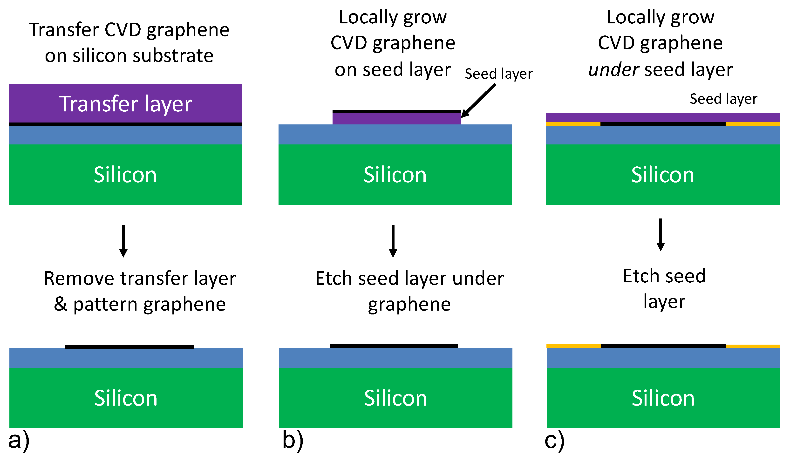
Abstract
:1. Introduction
1.1. Transfer-Based Integration
1.2. Transfer-Free Integration
1.3. Integration of Graphene Grown on Platinum
2. Methods
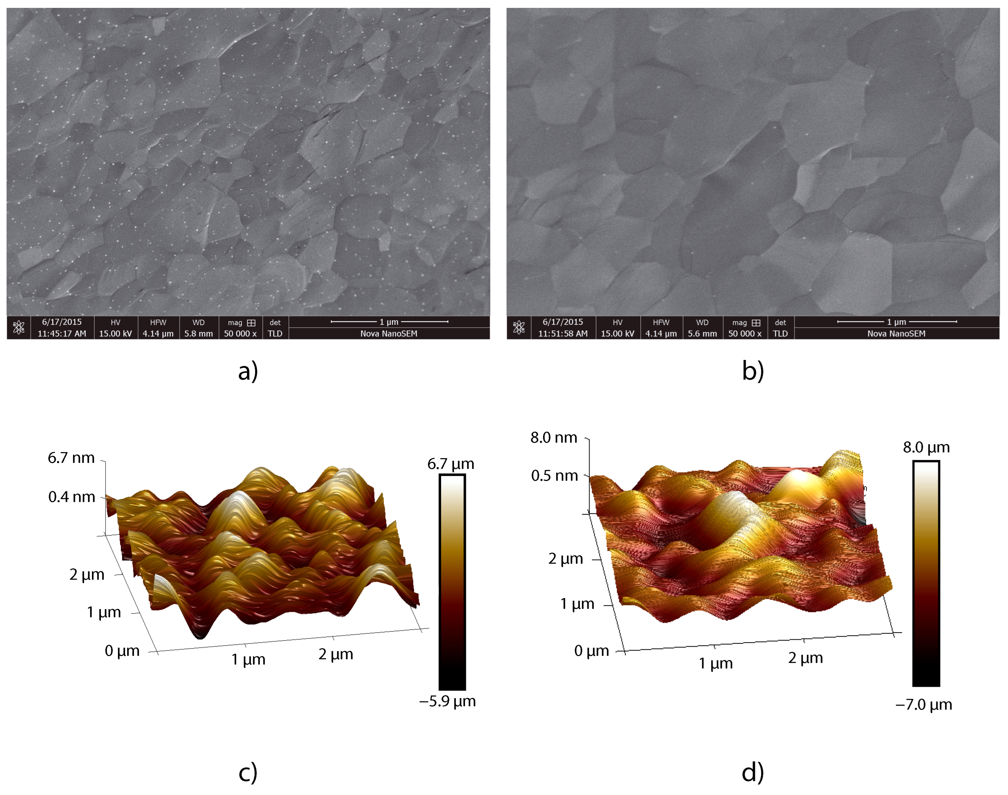
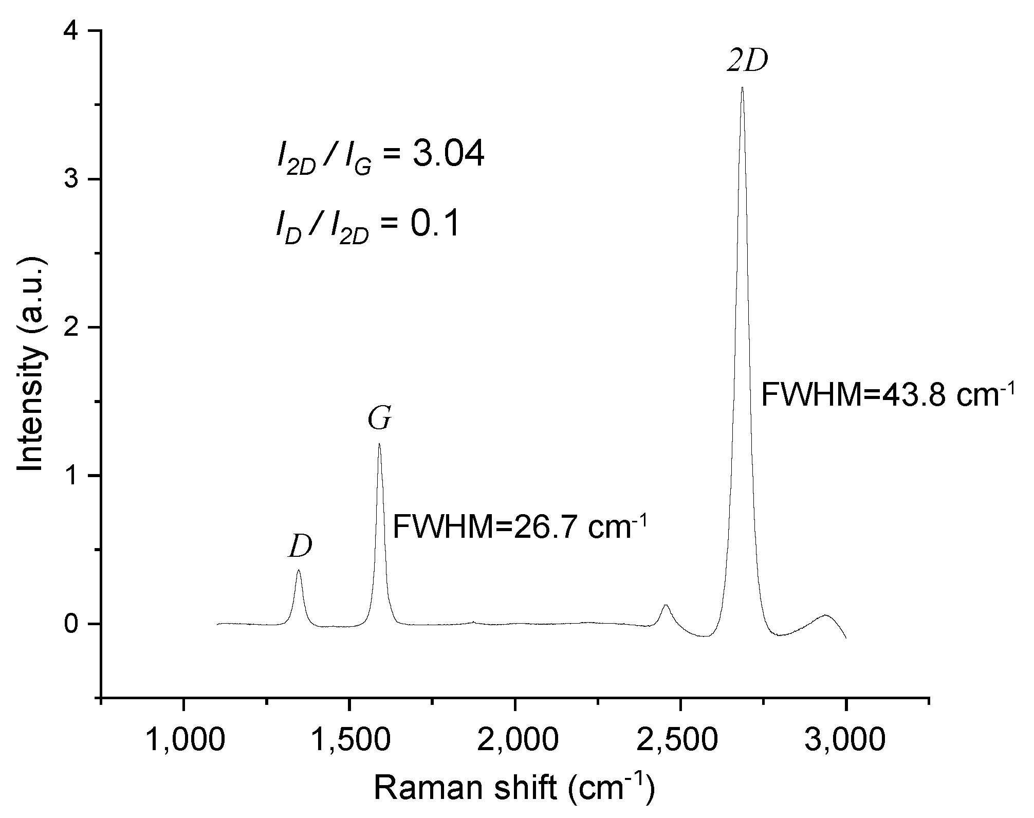
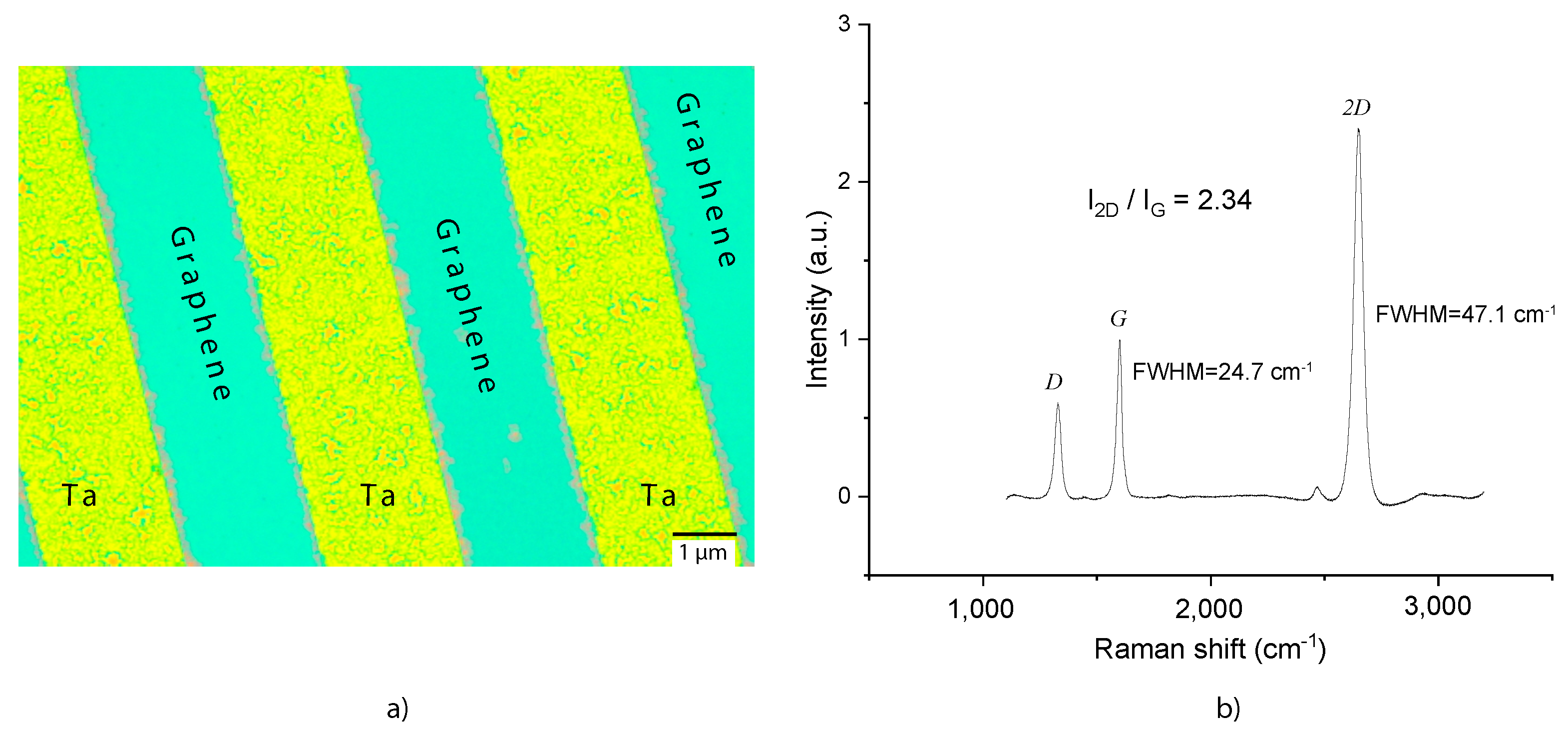
3. Results
4. Discussion
5. Conclusions
Author Contributions
Funding
Data Availability Statement
Acknowledgments
Conflicts of Interest
References
- Akinwande, D.; Huyghebaert, C.; Wang, C.H.; Serna, M.I.; Goossens, S.; Li, L.J.; Wong, H.S.P.; Koppens, F.H. Graphene and two-dimensional materials for silicon technology. Nature 2019, 573, 507–518. [Google Scholar] [CrossRef] [PubMed]
- Neumaier, D.; Pindl, S.; Lemme, M.C. Integrating graphene into semiconductor fabrication lines. Nat. Mater. 2019, 18, 525–529. [Google Scholar] [CrossRef] [PubMed] [Green Version]
- Ullah, S.; Yang, X.; Ta, H.Q.; Hasan, M.; Bachmatiuk, A.; Tokarska, K.; Trzebicka, B.; Fu, L.; Rummeli, M.H. Graphene transfer methods: A review. Nano Res. 2021, 14, 3756–3772. [Google Scholar] [CrossRef]
- Wagner, S.; Weisenstein, C.; Smith, A.D.; Östling, M.; Kataria, S.; Lemme, M.C. Graphene transfer methods for the fabrication of membrane-based NEMS devices. Microelectron. Eng. 2016, 159, 108–113. [Google Scholar] [CrossRef]
- Zhu, W.; Low, T.; Perebeinos, V.; Bol, A.A.; Zhu, Y.; Yan, H.; Tersoff, J.; Avouris, P. Structure and elctronic transport in graphene wrinkles. Nano Lett. 2012, 12, 3431–3436. [Google Scholar] [CrossRef] [Green Version]
- Grachova, Y.; Vollebregt, S.; Lacaita, A.L.; Sarro, P.M. High Quality Wafer-scale CVD Graphene on Molybdenum Thin Film for Sensing Application. Procedia Eng. 2014, 87, 1501–1504. [Google Scholar] [CrossRef]
- Ricciardella, F.; Vollebregt, S.; Polichetti, T.; Alfano, B.; Massera, E.; Sarro, P.M. High sensitive gas sensors realized by a transfer-free process of CVD graphene. In Proceedings of the 2016 IEEE SENSORS, Orlando, FL, USA, 30 October–3 November 2016; pp. 1–3. [Google Scholar] [CrossRef] [Green Version]
- Vollebregt, S.; Alfano, B.; Ricciardella, F.; Giesbers, A.J.M.; Grachova, Y.; van Zeijl, H.W.; Polichetti, T.; Sarro, P.M. A transfer-free wafer-scale CVD graphene fabrication process for MEMS/NEMS sensors. In Proceedings of the 2016 IEEE 29th International Conference on Micro Electro Mechanical Systems (MEMS), Shanghai, China, 24–28 January 2016; pp. 17–20. [Google Scholar] [CrossRef]
- Vollebregt, S.; Dolleman, R.J.; van der Zant, H.S.J.; Steeneken, P.G.; Sarro, P.M. Suspended graphene beams with tunable gap for squeeze-film pressure sensing. In Proceedings of the 2017 19th International Conference on Solid-State Sensors, Actuators and Microsystems (TRANSDUCERS), Kaohsiung, Taiwan, 18–22 June 2017; pp. 770–773. [Google Scholar] [CrossRef]
- Romijn, J.; Dolleman, R.J.; Singh, M.; van der Zant, H.S.J.; Steeneken, P.G.; Sarro, P.M.; Vollebregt, S. Multi-layer graphene pirani pressure sensors. Nanotechnology 2021, 32, 335501. [Google Scholar] [CrossRef]
- McNerny, D.Q.; Viswanath, B.; Copic, D.; Laye, F.R.; Prohoda, C.; Brieland-Shoultz, A.C.; Polsen, E.S.; Dee, N.T.; Veerasamy, V.S.; Hart, A.J. Direct fabrication of graphene on SiO2 enabled by thin film stress engineering. Sci. Rep. 2014, 4, 5049. [Google Scholar] [CrossRef] [Green Version]
- Kang, B.J.; Mun, J.H.; Hwang, C.Y.; Cho, B.J. Monolayer graphene growth on sputtered thin film platinum. J. Appl. Phys. 2009, 106, 104309. [Google Scholar] [CrossRef] [Green Version]
- Sutter, P.; Sadowski, J.T.; Sutter, E. Graphene on Pt (111): Growth and substrate interaction. Phys. Rev. B 2009, 80, 245411. [Google Scholar] [CrossRef] [Green Version]
- Gao, M.; Pan, Y.; Huang, L.; Hu, H.; Zhang, L.; Guo, H.; Du, S.; Gao, H.J. Epitaxial growth and structural property of graphene on Pt (111). Appl. Phys. Lett. 2011, 98, 033101. [Google Scholar] [CrossRef]
- Gao, T.; Xie, S.; Gao, Y.; Liu, M.; Chen, Y.; Zhang, Y.; Liu, Z. Growth and atomic-scale characterizations of graphene on multifaceted textured Pt foils prepared by chemical vapor deposition. ACS Nano 2011, 5, 9194–9201. [Google Scholar] [CrossRef] [PubMed]
- Addou, R.; Batzill, M. Defects and domain boundaries in self-assembled terephthalic acid (TPA) monolayers on CVD-grown graphene on Pt (111). Langmuir 2013, 29, 6354–6360. [Google Scholar] [CrossRef] [PubMed]
- Lee, B.J.; Jeong, G.H. Comparative study on graphene growth mechanism using Ni films, Ni/Mo sheets, and Pt substrates. Appl. Phys. A 2014, 116, 15–24. [Google Scholar] [CrossRef]
- Ma, T.; Ren, W.; Liu, Z.; Huang, L.; Ma, L.P.; Ma, X.; Zhang, Z.; Peng, L.M.; Cheng, H.M. Repeated growth–etching–regrowth for large-area defect-free single-crystal graphene by chemical vapor deposition. ACS Nano 2014, 8, 12806–12813. [Google Scholar] [CrossRef] [PubMed]
- Weatherup, R.S.; Shahani, A.J.; Wang, Z.J.; Mingard, K.; Pollard, A.J.; Willinger, M.G.; Schloegl, R.; Voorhees, P.W.; Hofmann, S. In situ graphene growth dynamics on polycrystalline catalyst foils. Nano Lett. 2016, 16, 6196–6206. [Google Scholar] [CrossRef]
- Preobrajenski, A.; Ng, M.L.; Vinogradov, A.; Mårtensson, N. Controlling graphene corrugation on lattice-mismatched substrates. Phys. Rev. B 2008, 78, 073401. [Google Scholar] [CrossRef]
- Xu, Z.; Buehler, M.J. Interface structure and mechanics between graphene and metal substrates: A first-principles study. J. Phys. Condens. Matter 2010, 22, 485301. [Google Scholar] [CrossRef]
- Gao, M.; Pan, Y.; Zhang, C.; Hu, H.; Yang, R.; Lu, H.; Cai, J.; Du, S.; Liu, F.; Gao, H.J. Tunable interfacial properties of epitaxial graphene on metal substrates. Appl. Phys. Lett. 2010, 96, 053109. [Google Scholar] [CrossRef]
- Adamska, L.; Lin, Y.; Ross, A.J.; Batzill, M.; Oleynik, I.I. Atomic and electronic structure of simple metal/graphene and complex metal/graphene/metal interfaces. Phys. Rev. B 2012, 85, 195443. [Google Scholar] [CrossRef] [Green Version]
- Verguts, K.; Coroa, J.; Huyghebaert, C.; De Gendt, S.; Brems, S. Graphene delamination using ‘electrochemical methods’: An ion intercalation effect. Nanoscale 2018, 10, 5515–5521. [Google Scholar] [CrossRef] [PubMed]
- Verguts, K.; Defossez, Y.; Leonhardt, A.; De Messemaeker, J.; Schouteden, K.; Van Haesendonck, C.; Huyghebaert, C.; De Gendt, S.; Brems, S. Growth of millimeter-sized graphene single crystals on Al2O3 (0001)/Pt (111) template wafers using chemical vapor deposition. ECS J. Solid State Sci. Technol. 2018, 7, M195. [Google Scholar] [CrossRef]
- Mafra, D.; Samsonidze, G.; Malard, L.; Elias, D.C.; Brant, J.; Plentz, F.; Alves, E.S.; Pimenta, M.A. Determination of LA and TO phonon dispersion relations of graphene near the Dirac point by double resonance Raman scattering. Phys. Rev. B 2007, 76, 233407. [Google Scholar] [CrossRef]
- Malard, L.; Pimenta, M.A.; Dresselhaus, G.; Dresselhaus, M. Raman spectroscopy in graphene. Phys. Rep. 2009, 473, 51–87. [Google Scholar] [CrossRef]
- Armano, A.; Agnello, S. Two-dimensional carbon: A review of synthesis methods, and electronic, optical, and vibrational properties of single-layer graphene. C 2019, 5, 67. [Google Scholar] [CrossRef] [Green Version]
- Seah, C.M.; Chai, S.P.; Mohamed, A.R. Mechanisms of graphene growth by chemical vapour deposition on transition metals. Carbon 2014, 70, 1–21. [Google Scholar] [CrossRef]
- Sun, B.; Pang, J.; Cheng, Q.; Zhang, S.; Li, Y.; Zhang, C.; Sun, D.; Ibarlucea, B.; Li, Y.; Chen, D.; et al. Synthesis of Wafer-Scale Graphene with Chemical Vapor Deposition for Electronic Device Applications. Adv. Mater. Technol. 2021, 6, 2000744. [Google Scholar] [CrossRef]
- Fairbrother, D.H.; Peng, X.; Viswanathan, R.; Stair, P.; Trenary, M.; Fan, J. Carbon-carbon coupling of methyl groups on Pt (111). Surf. Sci. Lett. 1993, 285, L455–L460. [Google Scholar] [CrossRef]
- Meixner, D.L.; George, S.M. Coverage dependent surface diffusion of noble gases and methane on Pt (111). Surf. Sci. 1993, 297, 27–39. [Google Scholar] [CrossRef]
- Liao, M.S.; Au, C.T.; Ng, C.F. Methane dissociation on Ni, Pd, Pt and Cu metal (111) surfaces—A theoretical comparative study. Chem. Phys. Lett. 1997, 272, 445–452. [Google Scholar] [CrossRef]
- Moussounda, P.; Haroun, M.; M’Passi-Mabiala, B.; Légaré, P. A DFT investigation of methane molecular adsorption on Pt (1 0 0). Surf. Sci. 2005, 594, 231–239. [Google Scholar] [CrossRef]
- Moussounda, P.; Haroun, M.; Rakotovelo, G.; Légaré, P. A theoretical study of CH4 dissociation on Pt (100) surface. Surf. Sci. 2007, 601, 3697–3701. [Google Scholar] [CrossRef]
- Selman, G.; Ellison, P.; Darling, A. Carbon in platinum and palladium. Platin. Met. Rev. 1970, 14, 14–20. [Google Scholar]
- Zhou, Q.; Coh, S.; Cohen, M.L.; Louie, S.G.; Zettl, A. Imprint of transition metal d orbitals on a graphene Dirac cone. Phys. Rev. B 2013, 88, 235431. [Google Scholar] [CrossRef] [Green Version]
- Rafaja, D.; Lengauer, W.; Wisenberger, H. Non-metal diffusion coefficients for the Ta-C and Ta-N systems. Acta Mater. 1998, 46, 3477–3483. [Google Scholar] [CrossRef]

Publisher’s Note: MDPI stays neutral with regard to jurisdictional claims in published maps and institutional affiliations. |
© 2022 by the authors. Licensee MDPI, Basel, Switzerland. This article is an open access article distributed under the terms and conditions of the Creative Commons Attribution (CC BY) license (https://creativecommons.org/licenses/by/4.0/).
Share and Cite
Hagendoorn, Y.; Pandraud, G.; Vollebregt, S.; Morana, B.; Sarro, P.M.; Steeneken, P.G. Direct Wafer-Scale CVD Graphene Growth under Platinum Thin-Films. Materials 2022, 15, 3723. https://doi.org/10.3390/ma15103723
Hagendoorn Y, Pandraud G, Vollebregt S, Morana B, Sarro PM, Steeneken PG. Direct Wafer-Scale CVD Graphene Growth under Platinum Thin-Films. Materials. 2022; 15(10):3723. https://doi.org/10.3390/ma15103723
Chicago/Turabian StyleHagendoorn, Yelena, Gregory Pandraud, Sten Vollebregt, Bruno Morana, Pasqualina M. Sarro, and Peter G. Steeneken. 2022. "Direct Wafer-Scale CVD Graphene Growth under Platinum Thin-Films" Materials 15, no. 10: 3723. https://doi.org/10.3390/ma15103723
APA StyleHagendoorn, Y., Pandraud, G., Vollebregt, S., Morana, B., Sarro, P. M., & Steeneken, P. G. (2022). Direct Wafer-Scale CVD Graphene Growth under Platinum Thin-Films. Materials, 15(10), 3723. https://doi.org/10.3390/ma15103723