
Study on the Strip Warpage Issues Encountered in the Flip-Chip Process


Abstract
:1. Introduction
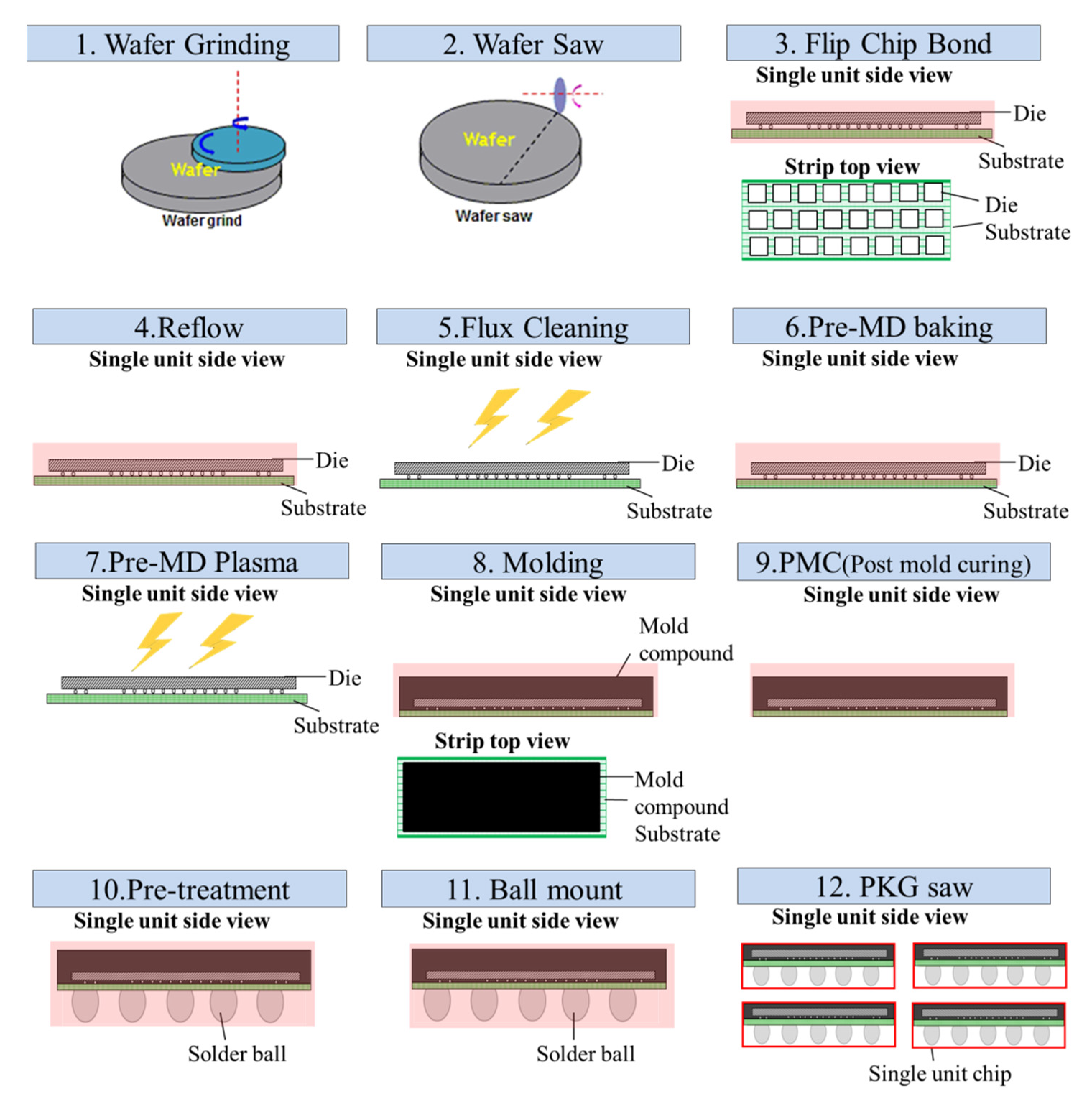
- Wafer Grinding: the wafer is first processed by grinding before any fabrication procedure is conducted.
- Wafer Saw: the wafer is diced into small dies of target size.
- Flip-chip Bond: the cut die obtained from Step 2 is placed on the substrate with the help of bumps and soldering flux, but these are not completely fused together.
- Reflow: through the reflow process, the bumps and soldering flux on the substrate are fused so that the die can be fixed on the substrate.
- Flux Cleaning: plasma cleaning can remove contaminants formed during the production process, thereby effectively enhancing the strength of the bond between the die and substrate.
- Pre-MD Baking: this refers to the baking before molding, where water moisture subsequently formed in the die, substrate, and bumps must be completely removed to ensure that the mold compound fits tightly to protect the die, substrate, and bumps.
- Pre-MD Plasma Cleaning: the plasma surface is cleaned to remove impurities on the surface so that gaps between the internal components can be filled during molding.
- Molding: a mold compound is injected into the package to seal all the components, protecting the die and bumps inside the device.
- Post-molding cure (PMC): the sealed device is cured again to enhance its structural stability.
- Pre-treatment: pre-heat treatment before implantation of solder balls.
- Ball Mounting and Reflow: solder balls are implanted underneath the base substrate for future signal connection with the external circuit.
- Package Saw: the strip is diced into single wafers for packaging and shipping.
2. Research Method
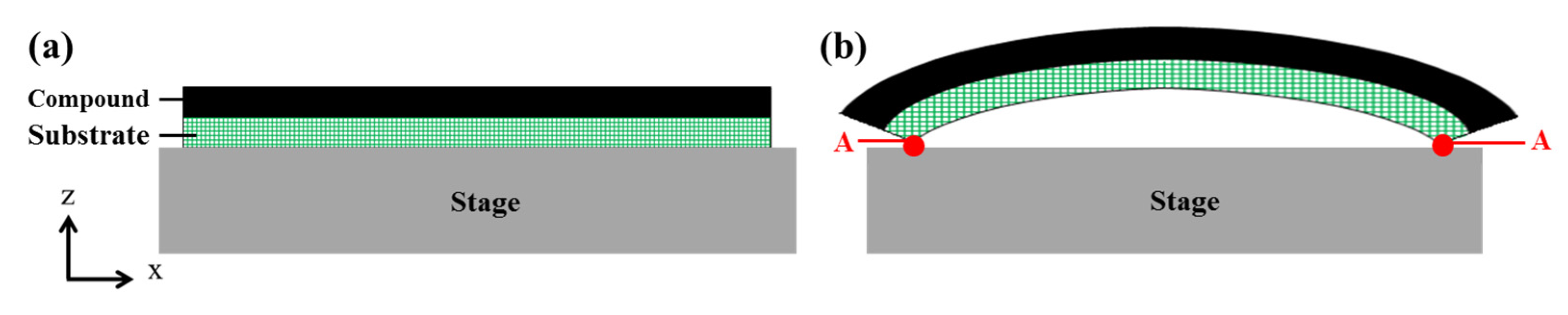
2.1. Strip Simulation Model
2.1.1. Model Establishment
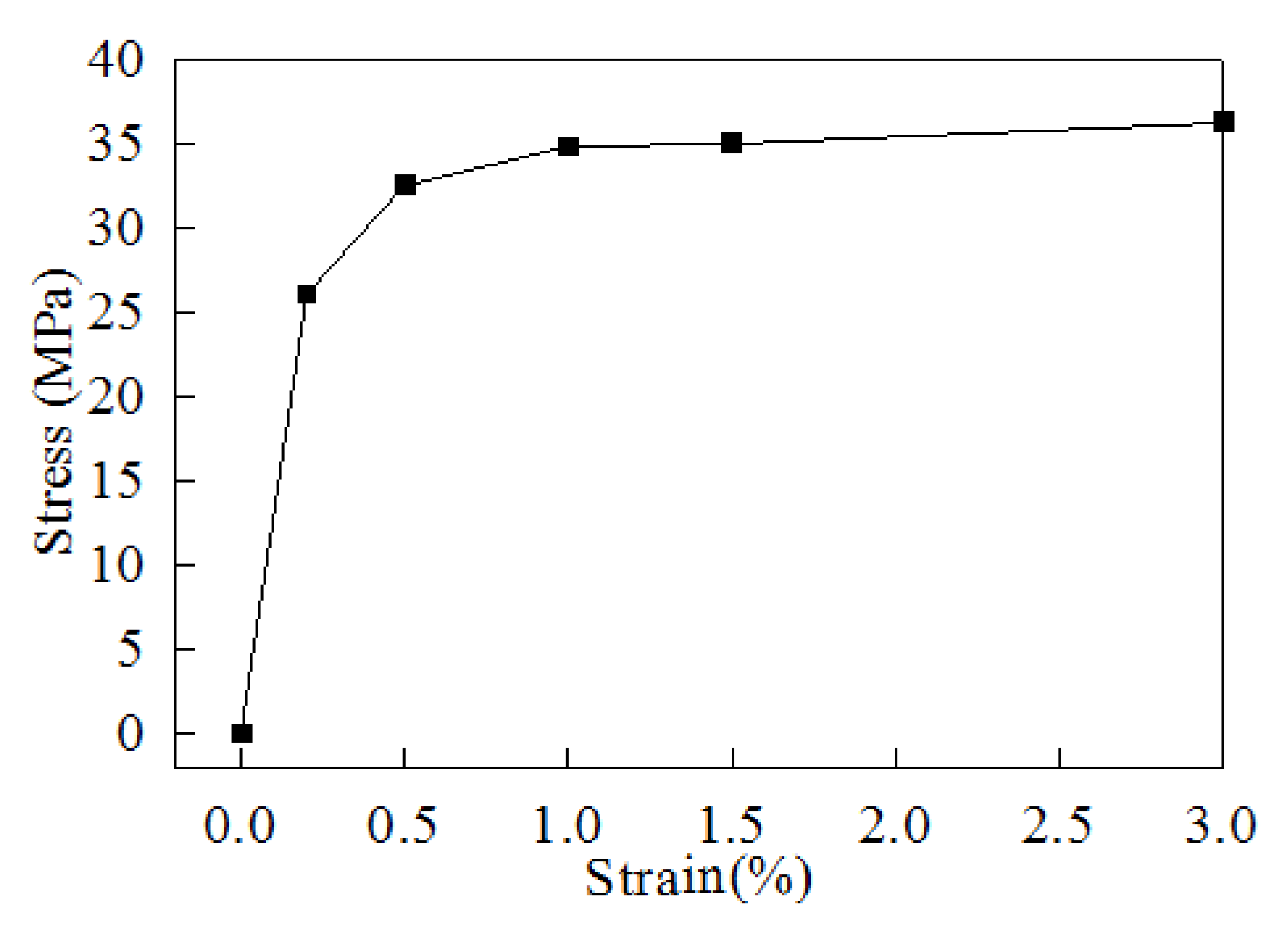
2.1.2. Establishing Material Parameters
2.1.3. Boundary Condition Settings
2.2. Taguchi Method
2.3. Structural Design
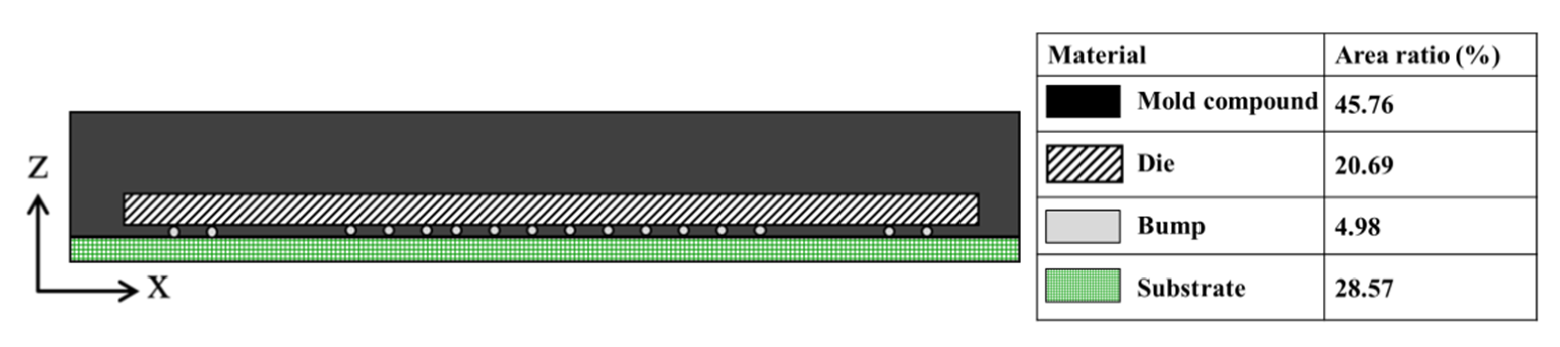
- A1 = AMold compound, n1 = nMold compound, z1 = zMold compound.
- A2 = ADie, n2 = nDie, z2 = zDie;
- A3 = ABump, n3 = nBump, z3 = zBump;
- A4 = ASubstrate, n4 = nSubstrate, z4 = zSubstrate.
3. Results
3.1. Experimental Results
3.2. Simulation Results
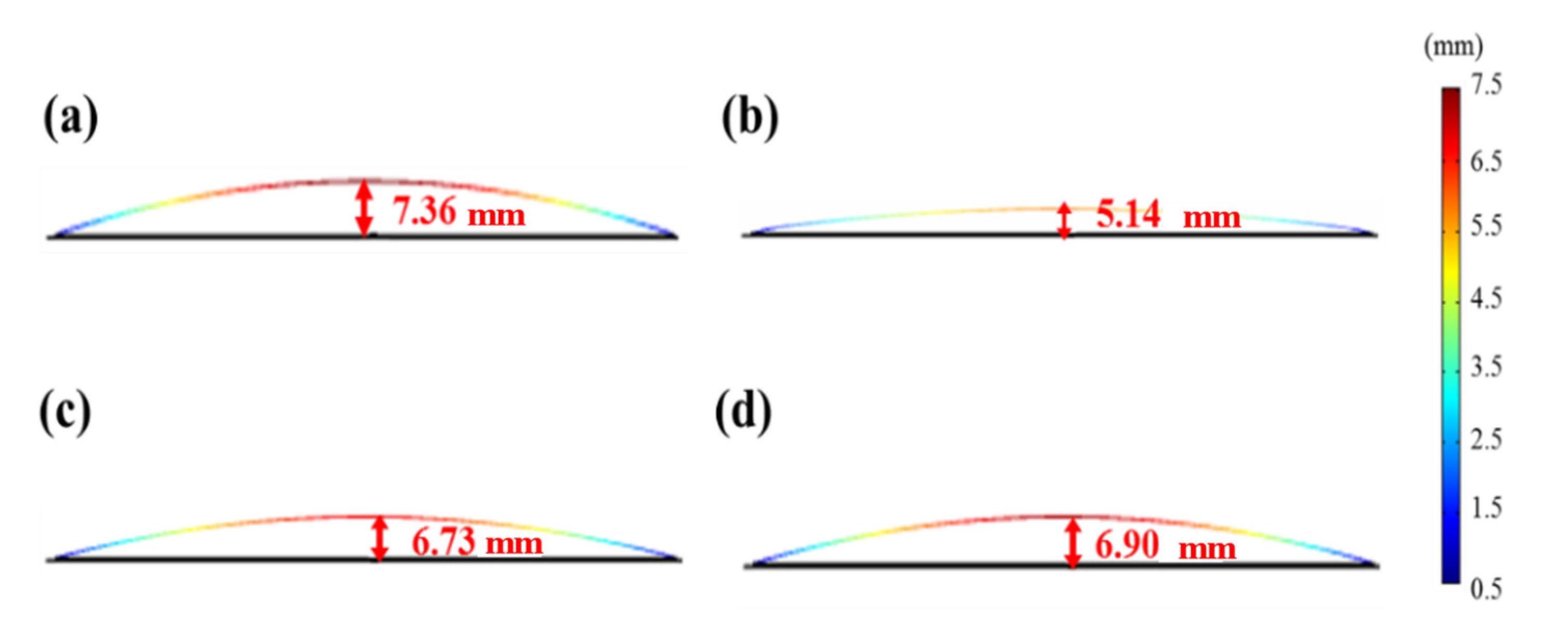
3.2.1. Experimental and Simulation Results
3.2.2. Comparison of Mold Compounds
- The CTE difference between the mold compound and substrate had a greater impact, the larger the difference, the larger the strip warpage.
- The Young’s modulus of the mold compound exerted an effect, the larger the young’s modulus, the greater the structural rigidity of the strip and the lower the warpage.
4. Discussion
4.1. Taguchi Analysis
- greater die thickness (>150 μm).
- greater mold compound thickness (>1100 μm).
- smaller substrate thickness (<100 μm); and
- lower molding temperature, although it should not be lower than the Tg of the mold compound.
4.2. Structural Design Criteria
- less warpage occurred when the substrate thickness was <180 μm (e.g., Nos. 16, 12, 6, 11, and 15) and the warpage was <5.15 mm.
- greater warpage occurred when the substrate thickness was ≥300 μm (e.g., Nos. 14, 7, 9, and 10) and the warpage was >7.92 mm; and
- Nos. 5 and 8 were special because the substrate thickness was only 180 μm (in No. 5), and the die thickness was only 75 μm, which caused insufficient structural rigidity, resulting in a warpage of 7.63 mm.
5. Conclusions
Author Contributions
Funding
Institutional Review Board Statement
Informed Consent Statement
Data Availability Statement
Acknowledgments
Conflicts of Interest
References
- Timoshenko, S. Analysis of Bi-Metal Thermostats. J. Opt. Soc. Am. 1925, 11, 233–255. [Google Scholar] [CrossRef]
- Chen, C.S. Different Conservation Laws Constructed on Warpage Analyses for Bimaterial Plates With Temperature-Dependent Properties. J. Electron. Packag. 2011, 133, 1–14. [Google Scholar] [CrossRef]
- Elevated Temperature Measurements of Warpage of BGA Package. Available online: https://akrometrix.com/wp-content/uploads/2016/02/Elevated-Temp-BGA-Warpage-Measurements.pdf (accessed on 1 July 2021).
- Wang, Z.; Wang, X.; Zhao, N.; He, J.; Wang, S.; Wu, G.; Cheng, Y. The desirable dielectric properties and high thermal conductivity of epoxy composites with the cobweb-structured SiCnw–SiO2–NH2 hybrids. J. Mater. Sci. Mater. Electron. 2021, 32, 20973–20984. [Google Scholar] [CrossRef]
- Wang, Z.; Wang, X.; Wang, S.; He, J.; Zhang, T.; Wang, J.; Wu, G. Simultaneously Enhanced Thermal Conductivity and Dielectric Breakdown Strength in Sandwich AlN/Epoxy Composites. Nanomaterials 2021, 11, 1898. [Google Scholar] [CrossRef] [PubMed]
- Wang, J.; Jia, Z.; Liu, X.; Dou, J.; Xu, B.; Wang, B.; Wu, G. Construction of 1D Heterostructure NiCo@C/ZnO Nanorod with Enhanced Microwave Absorption. Nanomicro Lett. 2021, 13, 175. [Google Scholar] [CrossRef] [PubMed]
- Zhou, X.; Jia, Z.; Zhang, X.; Wang, B.; Liu, X.; Xu, B.; Bi, L.; Wu, G. Electromagnetic wave absorption performance of NiCo2X4 (X = O, S, Se, Te) spinel structures. Chem. Eng. J. 2021, 420, 129907. [Google Scholar] [CrossRef]
- Dudek, R.; Walter, H.; Auersperg, J.; Michel, B. Numerical Analysis for Thermo-Mechanical Reliability of Polymers in Electronic Packaging. In Proceedings of the Polytronic 6th International Conference on Polymers and Adhesives in Microelectronics and Photonics, Tokyo, Japan, 15–18 January 2007; pp. 220–227. [Google Scholar]
- Hu, G.; Chew, S.; Singh, B. Cure Shrinkage Analysis of Green Epoxy Molding Compound with Application to Warpage Analysis in a Plastic IC Package. In Proceedings of the 8th International Conference on Electronic Packaging Technology, Shanghai, China, 14–17 August 2007; pp. 1–5. [Google Scholar]
- Huang, C.Y.; Li, T.D.; Tsai, M.Y. Warpage measurement and design of wBGA package under thermal loading. In Proceedings of the 4th International Microsystems, Packaging, Assembly and Circuits Technology Conference, Taipei, Taiwan, 21–23 October 2009; pp. 415–418. [Google Scholar]
- Chae, M.; Ouyang, E. Strip warpage analysis of a flip chip package considering the mold compound processing parameters. In Proceedings of the IEEE 63rd Electronic Components and Technology Conference, Las Vegas, NV, USA, 28–31 May 2013; pp. 441–448. [Google Scholar]
- Huber, S.; von Dijk, M.; Walter, H.; Wittler, O.; Thomas, T.; Lang, K.D. Improving the FE simulation of molded packages using warpage measurements. Microelectron. Reliab. 2014, 54, 1862–1866. [Google Scholar] [CrossRef]
- Bin, G.; Dimaano, J.; Chen, R.; Bool, E.; Shi, S.F.; Ang, C.G.; Suthiwongsunthorn, N. Unit warpage control with universal die thickness. In Proceedings of the IEEE 16th Electronics Packaging Technology Conference, Singapore, 3–5 December 2014; pp. 303–306. [Google Scholar]
- Zheng, J.; Zhou, E.; Wang, L.; Aldrete, M.; Kumar, R.; Syed, A. Relative and absolute warpage modeling on molded packages. In Proceedings of the IEEE 65th Electronic Components and Technology Conference, San Diego, CA, USA, 26–29 May 2015; pp. 1538–1545. [Google Scholar]
- Chen, C.; Yu, D.Q.; Wang, T.; Xiao, Z.Y.; Wan, L.X. Warpage Prediction and Optimization for Embedded Silicon Fan-Out Wafer-Level Packaging Based on an Extended Theoretical Model. IEEE Trans. Compon. Packag. Manuf. Technol. 2019, 9, 845–853. [Google Scholar] [CrossRef]
- Tsai, M.Y.; Wang, Y.W. A Theoretical Solution for Thermal Warpage of Flip-Chip Packages. IEEE Trans. Compon. Packag. Manuf. Technol. 2020, 10, 72–78. [Google Scholar] [CrossRef]
- Tsai, M.Y.; Wang, Y.W.; Liu, C.M. Thermally Induced Deformations and Warpages of Flip-Chip and 2.5D IC Packages Measured by Strain Gauges. Materials 2021, 14, 3723. [Google Scholar] [CrossRef] [PubMed]
- Yao, X.J.; Fang, J.J.; Zhang, W. A Further Study on the Analytical Model for the Permeability in Flip-Chip Packaging. J. Electron. Packag. 2018, 140, 011001–011006. [Google Scholar] [CrossRef]
- Yao, X.; Jiang, W.; Yang, J.; Fang, J.; Zhang, W. A Surface Energy Approach to Developing an Analytical Model for the Underfill Flow Process in Flip-Chip Packaging. J. Electron. Packag. 2021, 144, 041003–041014. [Google Scholar] [CrossRef]
- Panigrahy, S.K.; Tseng, Y.C.; Lai, B.R.; Chiang, K.N. An Overview of AI-Assisted Design-on-Simulation Technology for Reliability Life Prediction of Advanced Packaging. Materials 2021, 14, 5342. [Google Scholar] [CrossRef] [PubMed]
- Lin, P.Y.; Lee, S. Warpage Modeling of Ultra-Thin Packages Based on Chemical Shrinkage and Cure-Dependent Viscoelasticity of Molded Underfill. IEEE Trans. Device Mater. Reliab. 2020, 20, 67–73. [Google Scholar] [CrossRef]
- Cheng, H.C.; Tai, L.C.; Liu, Y.C. Theoretical and Experimental Investigation of Warpage Evolution of Flip Chip Package on Packaging during Fabrication. Materials 2021, 14, 4816. [Google Scholar] [CrossRef] [PubMed]
- IPC-4101: Specification for Base Materials for Rigid and Multilayer Printed Boards. Available online: https://www.ipc.org/TOC/TOC-IPC-4101E.pdf (accessed on 1 July 2021).
- Hibbeler, R.C. Mechanics of Materials, 9th ed.; Pearson: London, UK, 2014. [Google Scholar]
- Yeh, C.; Lai, Y. A numerical approach towards the correlation between ball impact test and drop reliability. In Proceedings of the 8th Electronics Packaging Technology Conference, Singapore, 6–8 December 2006; pp. 161–167. [Google Scholar]
- Syed, A. Accumulated creep strain and energy density based thermal fatigue life prediction models for SnAgCu solder joints. In Proceedings of the 54th Electronic Components and Technology Conference, Las Vegas, NV, USA, 4 June 2004; pp. 737–746. [Google Scholar]
- Chuang, W.C.; Chen, W.L. Investigation of Strip Warpage Behavior in Wire Bonding Process. J. Electron. Packag. 2020, 142, 021002–021014. [Google Scholar] [CrossRef]


| PKG Information | |
|---|---|
| PKG size (mm2) | 7 × 7 |
| Mold compound thickness (µm) | 450 |
| Die size (mm2) | 6.3 × 6.34 |
| Die thickness (µm) | 150 |
| Bump type | SAC405 |
| Bump pitch (µm) | 190 |
| Process Flow | Strip Warpage (mm) | ||
|---|---|---|---|
| Long Side (x-Direction) | Short Side (y-Direction) | ||
| 8. Molding | 175 °C | 0 | 0 |
| 25 °C | 7 | 0 | |
| 9. PMC | 5 | N/A | |
| 10. Pre-treatment | 7 | N/A | |
| 11. Ball mount | 7.5 | N/A | |
| Process Flow | Strip Warpage (mm) | ||
|---|---|---|---|
| Experimental Value | Simulation Value | ||
| 8. Molding | 175 °C | 0 | 0 |
| 25 °C | 7 | 7.36 | |
| 9. PMC | 5 | 5.14 | |
| 10. Pre-treatment | 7 | 6.73 | |
| 11. Ball mount | 7.5 | 6.90 | |
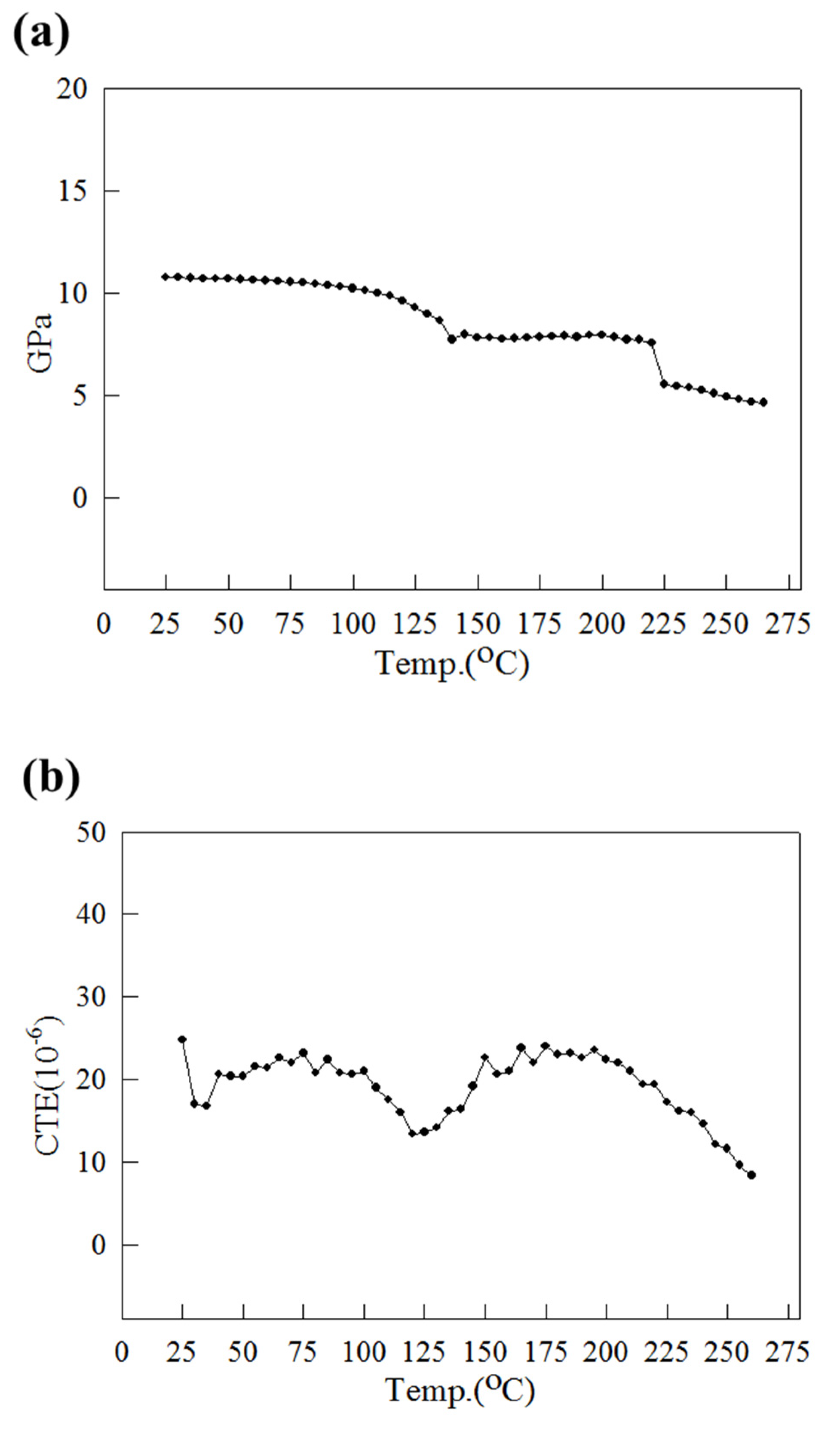
| Bump-SAC405 | Die (Silicon100) | Substrate | |
|---|---|---|---|
| Young’s modulus (GPa) | 53 | 131 | Figure 5a |
| Poisson’s ratio | 0.40805 | 0.27 | 0.2 |
| Density (kg/m3) | 7445.45 | 2330 | 1938 |
| CTE (ppm/°C) | 20 | 2.8 | Figure 5b |
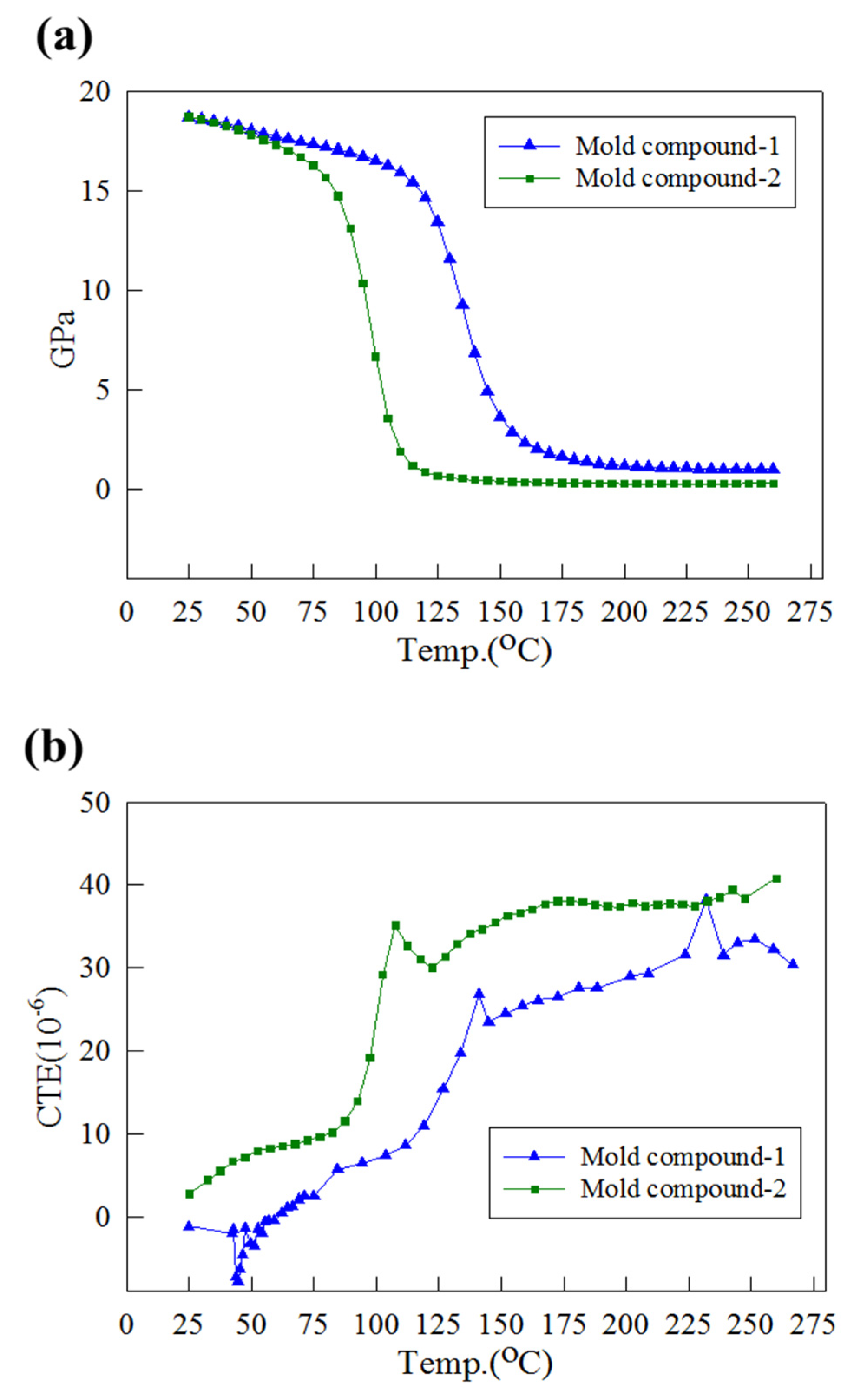
| Mold Compound 1 | Mold Compound 2 | |
|---|---|---|
| Young’s modulus (GPa) | Figure 6a | Figure 6a |
| Poisson’s ratio | 0.3 | 0.3 |
| Density (kg/m3) | 2010 | 1990 |
| CTE (ppm/°C) | Figure 6b | Figure 6b |
| Process Flow | Temperature Range (°C) | Process Time (s) |
|---|---|---|
| 8. Molding | 175 → 25 | 30 |
| 9. PMC | 25 → 175 → 25 | 20040 |
| 10. Pre-treatment | 25 → 238 → 25 | 935 |
| 11. Ball mount | 25 → 238 → 25 | 935 |
| Name of Control Factors | Level 1 | Level 2 | Level 3 | Level 4 |
|---|---|---|---|---|
| Mold compound thickness(µm) | 150 | 450 | 750 | 1100 |
| Die thickness (µm) | 75 | 150 | 250 | 400 |
| Substrate thickness(µm) | 100 | 180 | 300 | 500 |
| Molding temp. (°C) | 150 | 165 | 175 | 185 |
| PMC temp. (°C) | 175 | 185 |
| Material | Young’s Modulus (GPa) | n = Material (E)/Substrate (E) |
|---|---|---|
| Substrate | 10.75 | 1 |
| Bump | 53 | 4.93 |
| Die | 131 | 12.18 |
| Mold compound 1 | 18.66 | 1.73 |
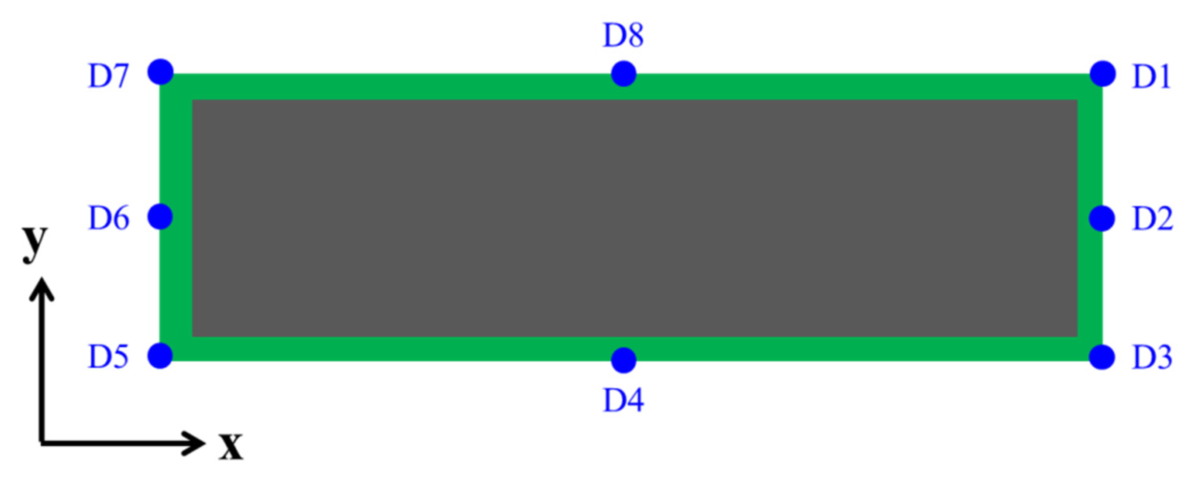
| Process Flow | Strip Warpage (mm) | ||||||||
|---|---|---|---|---|---|---|---|---|---|
| Long Side (x-Direction) | Short Side (y-Direction) | Corner | |||||||
| D4 | D8 | D2 | D6 | D1 | D3 | D5 | D7 | ||
| 8. Molding | 175 °C | 0 | 0 | 0 | 0 | 0 | 0 | 0 | 0 |
| 25 °C | 7 | 7 | 0 | 0 | 0 | 0 | 0 | 0 | |
| Process Flow | Strip Warpage (mm) | ||
|---|---|---|---|
| Experimental Value | Simulation Value | Error (%) | |
| 8. Molding | 7 | 7.36 | 5.14 |
| 9. PMC | 5 | 5.14 | 2.8 |
| 10. Pre-treatment | 7 | 6.73 | 3.85 |
| 11. Ball mount | 7.5 | 6.90 | 8.00 |
| Process Flow | Strip Warpage (mm) | |
|---|---|---|
| Mold Compound 1 | Mold Compound 2 | |
| 8. Molding | 7.36 | 5.02 |
| 9. PMC | 5.14 | 3.48 |
| 10. Pre-treatment | 6.73 | 4.65 |
| 11. Ball mount | 6.90 | 4.71 |
| No. | Mold Compound Thickness (µm) | Die Thickness (µm) | Substrate Thickness (µm) | Molding Temp. (°C) | PMC Temp. (°C) | Ball Mount Warpage (mm) | zn (µm) |
|---|---|---|---|---|---|---|---|
| Original | 450 | 150 | 180 | 175 | 175 | 6.36 | 280.61 |
| 1 | 150 | 75 | 100 | 150 | 175 | 4.69 | 156.18 |
| 2 | 150 | 150 | 180 | 165 | 175 | 6.21 | 258.21 |
| 3 | 150 | 250 | 300 | 175 | 185 | 7.71 | 410.69 |
| 4 | 150 | 400 | 500 | 185 | 185 | 7.47 | 661.20 |
| 5 | 450 | 75 | 180 | 175 | 185 | 7.63 | 264.51 |
| 6 | 450 | 150 | 100 | 185 | 185 | 4.47 | 205.25 |
| 7 | 450 | 250 | 500 | 150 | 175 | 8.31 | 602.85 |
| 8 | 450 | 400 | 300 | 165 | 175 | 4.75 | 479.12 |
| 9 | 750 | 75 | 300 | 185 | 175 | 9.36 | 434.78 |
| 10 | 750 | 150 | 500 | 175 | 175 | 9.79 | 620.90 |
| 11 | 750 | 250 | 100 | 165 | 185 | 4.81 | 276.04 |
| 12 | 750 | 400 | 180 | 150 | 185 | 2.94 | 394.61 |
| 13 | 1100 | 75 | 500 | 165 | 185 | 8.98 | 703.36 |
| 14 | 1100 | 150 | 300 | 150 | 185 | 7.92 | 524.47 |
| 15 | 1100 | 250 | 180 | 185 | 175 | 5.15 | 421.30 |
| 16 | 1100 | 400 | 100 | 175 | 175 | 1.91 | 373.81 |
Publisher’s Note: MDPI stays neutral with regard to jurisdictional claims in published maps and institutional affiliations. |
© 2022 by the authors. Licensee MDPI, Basel, Switzerland. This article is an open access article distributed under the terms and conditions of the Creative Commons Attribution (CC BY) license (https://creativecommons.org/licenses/by/4.0/).
Share and Cite
Chuang, W.-C.; Chen, W.-L. Study on the Strip Warpage Issues Encountered in the Flip-Chip Process. Materials 2022, 15, 323. https://doi.org/10.3390/ma15010323
Chuang W-C, Chen W-L. Study on the Strip Warpage Issues Encountered in the Flip-Chip Process. Materials. 2022; 15(1):323. https://doi.org/10.3390/ma15010323
Chicago/Turabian StyleChuang, Wan-Chun, and Wei-Long Chen. 2022. "Study on the Strip Warpage Issues Encountered in the Flip-Chip Process" Materials 15, no. 1: 323. https://doi.org/10.3390/ma15010323
APA StyleChuang, W.-C., & Chen, W.-L. (2022). Study on the Strip Warpage Issues Encountered in the Flip-Chip Process. Materials, 15(1), 323. https://doi.org/10.3390/ma15010323