Parasitic Current Induced by Gate Overlap in Thin-Film Transistors
Abstract
1. Introduction
2. Devices and Experiment
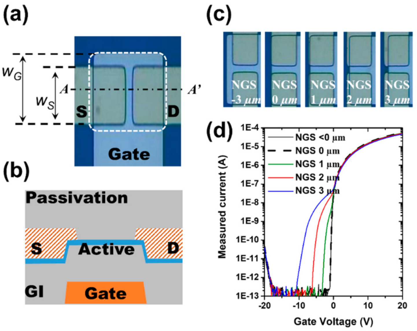
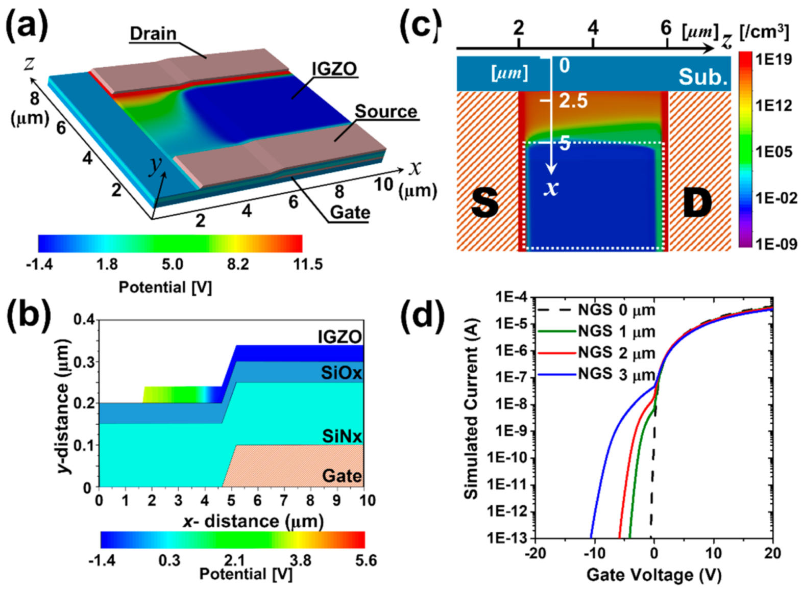
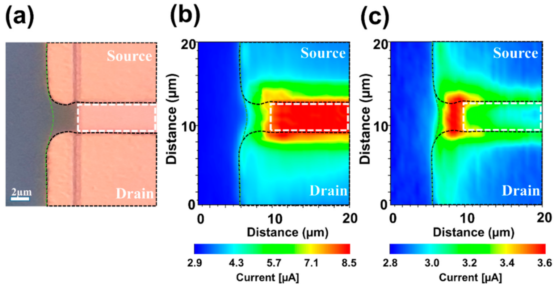
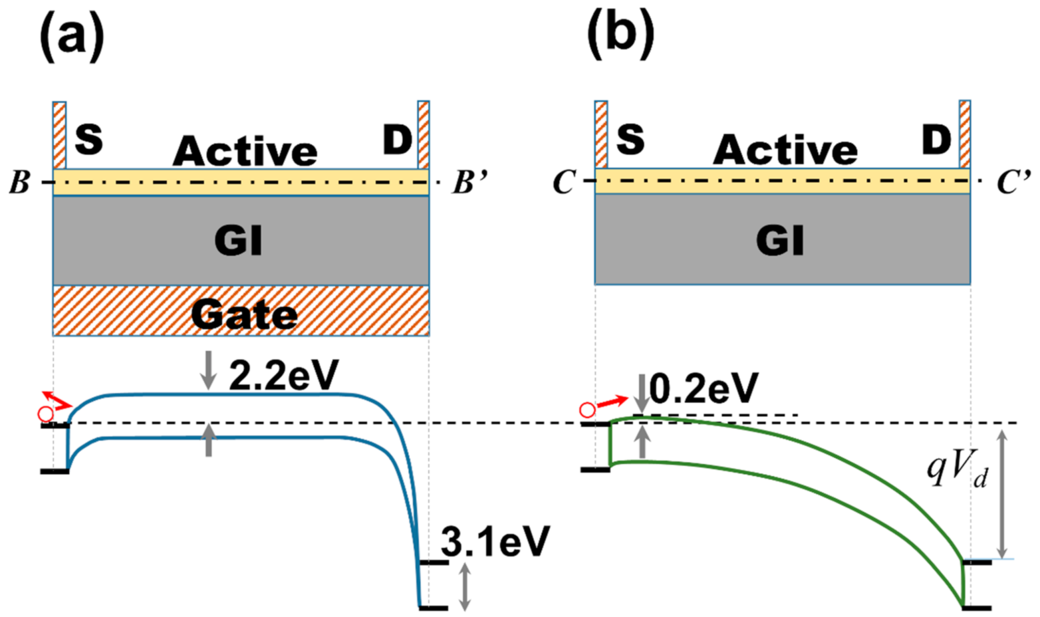
3. Results and Discussion
4. Conclusions
Author Contributions
Funding
Institutional Review Board Statement
Informed Consent Statement
Data Availability Statement
Conflicts of Interest
References
- Nomura, K.; Ohta, H.; Ueda, K.; Kamiya, T.; Hirano, M.; Hosono, H. Thin-film transistor fabricated in single-crystalline transparent oxide semiconductor. Science 2003, 300, 1269–1272. [Google Scholar] [CrossRef]
- Takahashi, T.; Fujii, M.N.; Miyanaga, R.; Miyanaga, M.; Ishikawa, Y.; Uraoka, Y. Unique degradation under AC stress in high-mobility amorphous In–W–Zn–O thin-film transistors. Appl. Phys. Express 2020, 13, 054003. [Google Scholar] [CrossRef]
- Lee, H.; Abe, K. A Study on the Effect of Pulse Rising and Falling Time on Amorphous Oxide Semiconductor Transistors in Driver Circuits. IEEE Electron Device Lett. 2020, 41, 896–899. [Google Scholar] [CrossRef]
- Takahashi, T.; Miyanaga, R.; Fujii, M.N.; Tanaka, J.; Takechi, K.; Tanabe, H.; Bermundo, J.P.; Ishikawa, Y.; Uraoka, Y. Hot carrier effects in InGaZnO thin-film transistor. Appl. Phys. Express 2019, 12, 094007. [Google Scholar] [CrossRef]
- Noh, H.Y.; Kim, J.; Kim, J.-S.; Lee, M.-J.; Lee, H.-J. Role of Hydrogen in Active Layer of Oxide-Semiconductor-Based Thin Film Transistors. Crystals 2019, 9, 75. [Google Scholar] [CrossRef]
- Hong, S.Y.; Kim, H.J.; Kim, D.H.; Jeong, H.Y.; Song, S.H.; Cho, I.T.; Noh, J.; Yun, P.S.; Lee, S.W.; Park, K.S.; et al. Study on the Lateral Carrier Diffusion and Source-Drain Series Resistance in Self-Aligned Top-Gate Coplanar InGaZnO Thin-Film Transistors. Sci. Rep. 2019, 9, 6588. [Google Scholar] [CrossRef] [PubMed]
- Yang, C.; Chang, T.; Liao, P.; Chen, L.; Chen, B.; Chou, W.; Chen, G.; Lin, S.; Yeh, C.; Tsai, C.; et al. Drain-Induced-Barrier-Lowing-Like Effect Induced by Oxygen-Vacancy in Scaling-Down via-Contact Type Amorphous InGaZnO Thin-Film Transistors. IEEE J. Electron Devices Soc. 2018, 6, 685–690. [Google Scholar] [CrossRef]
- Myny, K. The development of flexible integrated circuits based on thin-film transistors. Nat. Electron. 2018, 1, 30–39. [Google Scholar] [CrossRef]
- Chen, H.T.; Cao, Y.; Zhang, J.L.; Zhou, C.W. Large-scale complementary macroelectronics using hybrid integration of carbon nanotubes and IGZO thin-film transistors. Nat. Commun. 2014, 5, 4097. [Google Scholar] [CrossRef]
- Ide, K.; Nomura, K.; Hosono, H.; Kamiya, T. Electronic Defects in Amorphous Oxide Semiconductors: A Review. Phys. Status Solidi 2019, 216, 1800372. [Google Scholar] [CrossRef]
- Fortunato, E.; Barquinha, P.; Martins, R. Oxide semiconductor thin-film transistors: A review of recent advances. Adv. Mater. 2012, 24, 2945–2986. [Google Scholar] [CrossRef] [PubMed]
- Lee, H.-J.; Cho, S.H.; Abe, K.; Lee, M.-J.; Jung, M. Impact of transient currents caused by alternating drain stress in oxide semiconductors. Sci. Rep. 2017, 7, 9782–9790. [Google Scholar] [CrossRef]
- Lee, S.; Li, X.; Mativenga, M.; Jang, J. Bulk-Accumulation Oxide Thin-Film Transistor Circuits with Zero Gate-to-Drain Overlap Capacitance for High Speed. IEEE Electron Device Lett. 2015, 36, 1329–1331. [Google Scholar] [CrossRef]
- Jeong, J.; Hong, Y. Gate Overlap Optimization and Performance Variation for Thin-Film Transistors with Source/Drain Edge Waviness. Jpn. J. Appl. Phys. 2010, 49, 036501. [Google Scholar] [CrossRef]
- Lee, H.-J.; Abe, K.; Noh, H.Y.; Kim, J.-S.; Lee, H.; Lee, M.-J. Analysis of the hump phenomenon and needle defect states formed by driving stress in the oxide semiconductor. Sci. Rep. 2019, 9, 11977. [Google Scholar] [CrossRef]
- Mativenga, M.; Haque, F.; Um, J.G.; Siddik, A.B. Impact of Source-to-Gate and Drain-to-Gate Overlap Lengths on Performance of Inverted Staggered a-IGZO TFTs with an Etch Stopper. IEEE Trans. Electron Devices 2020, 67, 3152–3156. [Google Scholar] [CrossRef]
- Valletta, A.; Gaucci, P.; Mariucci, L.; Fortunato, G.; Templier, F. “Hump” characteristics and edge effects in polysilicon thin film transistors. J. Appl. Phys. 2008, 104, 124511. [Google Scholar] [CrossRef]
- Huang, C.F.; Peng, C.Y.; Yang, Y.J.; Sun, H.C.; Chang, H.C.; Kuo, P.S.; Chang, H.L.; Liu, C.Z.; Liu, C.W. Stress-Induced Hump Effects of p-Channel Polycrystalline Silicon Thin-Film Transistors. IEEE Electron Device Lett. 2008, 29, 1332–1335. [Google Scholar] [CrossRef]
- Mativenga, M.; Seok, M.; Jang, J. Gate bias-stress induced hump-effect in transfer characteristics of amorphous-indium-galium-zinc-oxide thin-fim transistors with various channel widths. Appl. Phys. Lett. 2011, 99, 122107. [Google Scholar] [CrossRef]
- Choi, S.-H.; Han, M.-K. Effect of channel widths on negative shift of threshold voltage, including stress-induced hump phenomenon in InGaZnO thin-film transistors under high-gate and drain bias stress. Appl. Phys. Lett. 2012, 100, 043503–043505. [Google Scholar] [CrossRef]
- Tsai, M.-Y.; Chang, T.-C.; Chu, A.-K.; Hsieh, T.-Y.; Chen, T.-C.; Lin, K.-Y.; Tsai, W.-W.; Chiang, W.-J.; Yan, J.-Y. High temperature-induced abnormal suppression of sub-threshold swing and on-current degradations under hot-carrier stress in a-InGaZnO thin film transistors. Appl. Phys. Lett. 2013, 103, 012101. [Google Scholar] [CrossRef]
- Jeong, C.-Y.; Lee, D.; Song, S.-H.; Kim, J.I.; Lee, J.-H.; Kwon, H.-I. A study on the degradation mechanism of InGaZnO thin-film transistors under simultaneous gate and drain bias stresses based on the electronic trap characterization. Semicond. Sci. Technol. 2014, 29, 045023. [Google Scholar] [CrossRef]
- Hwarim, I.; Hyunsoo, S.; Jaewook, J.; Yewon, H.; Yongtaek, H. Effects of defect creation on bidirectional behavior with hump characteristics of InGaZnO TFTs under bias and thermal stress. Jpn. J. Appl. Phys. 2015, 54, 03CB03. [Google Scholar]
- Lee, H.-J.; Abe, K.; Kim, J.S.; Lee, M.-J. Electron-blocking by the potential barrier originated from the asymmetrical local density of state in the oxide semiconductor. Sci. Rep. 2017, 7, 17963–17970. [Google Scholar] [CrossRef] [PubMed]
- Lee, H.-J.; Abe, K.; Cho, S.H.; Kim, J.; Bang, S.; Lee, M. Drain-Induced Barrier Lowering in Oxide Semiconductor Thin-Film Transistors with Asymmetrical Local Density of States. IEEE J. Electron Devices Soc. 2018, 6, 830–834. [Google Scholar] [CrossRef]
- Furuta, M.; Kamada, Y.; Kimura, M.; Hiramatsu, T.; Matsuda, T.; Furuta, H.; Li, C.; Fujita, S.; Hirao, T. Analysis of Hump Characteristics in Thin-Film Transistors with ZnO Channels Deposited by Sputtering at Various Oxygen Partial Pressures. IEEE Electron Device Lett. 2010, 31, 1257–1259. [Google Scholar] [CrossRef]
- Lee, M.-J.; Ahn, J.-H.; Sung, J.H.; Heo, H.; Jeon, S.G.; Lee, W.; Song, J.Y.; Hong, K.-H.; Choi, B.; Lee, S.-H.; et al. Thermoelectric materials by using two-dimensional materials with negative correlation between electrical and thermal conductivity. Nat. Commun. 2016, 7, 12011. [Google Scholar] [CrossRef]
- Sze, S.M.; Li, Y.; Ng, K.K. Physics of Semiconductor Devices, 3rd ed.; John Wiley & Sons: Hoboken, NJ, USA, 2006. [Google Scholar]


Publisher’s Note: MDPI stays neutral with regard to jurisdictional claims in published maps and institutional affiliations. |
© 2021 by the authors. Licensee MDPI, Basel, Switzerland. This article is an open access article distributed under the terms and conditions of the Creative Commons Attribution (CC BY) license (https://creativecommons.org/licenses/by/4.0/).
Share and Cite
Lee, H.-J.; Abe, K.; Kim, J.-S.; Yun, W.S.; Lee, M.-J. Parasitic Current Induced by Gate Overlap in Thin-Film Transistors. Materials 2021, 14, 2299. https://doi.org/10.3390/ma14092299
Lee H-J, Abe K, Kim J-S, Yun WS, Lee M-J. Parasitic Current Induced by Gate Overlap in Thin-Film Transistors. Materials. 2021; 14(9):2299. https://doi.org/10.3390/ma14092299
Chicago/Turabian StyleLee, Hyeon-Jun, Katsumi Abe, June-Seo Kim, Won Seok Yun, and Myoung-Jae Lee. 2021. "Parasitic Current Induced by Gate Overlap in Thin-Film Transistors" Materials 14, no. 9: 2299. https://doi.org/10.3390/ma14092299
APA StyleLee, H.-J., Abe, K., Kim, J.-S., Yun, W. S., & Lee, M.-J. (2021). Parasitic Current Induced by Gate Overlap in Thin-Film Transistors. Materials, 14(9), 2299. https://doi.org/10.3390/ma14092299


