
Nanoscale Piezoelectric Properties and Phase Separation in Pure and La-Doped BiFeO3 Films Prepared by Sol–Gel Method


 , ,
, ,  and
and 
Abstract
1. Introduction
2. Materials and Methods
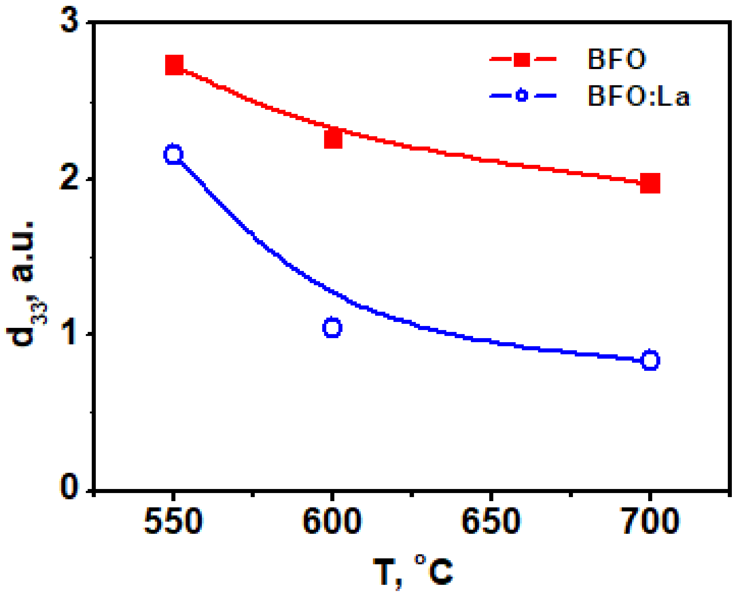
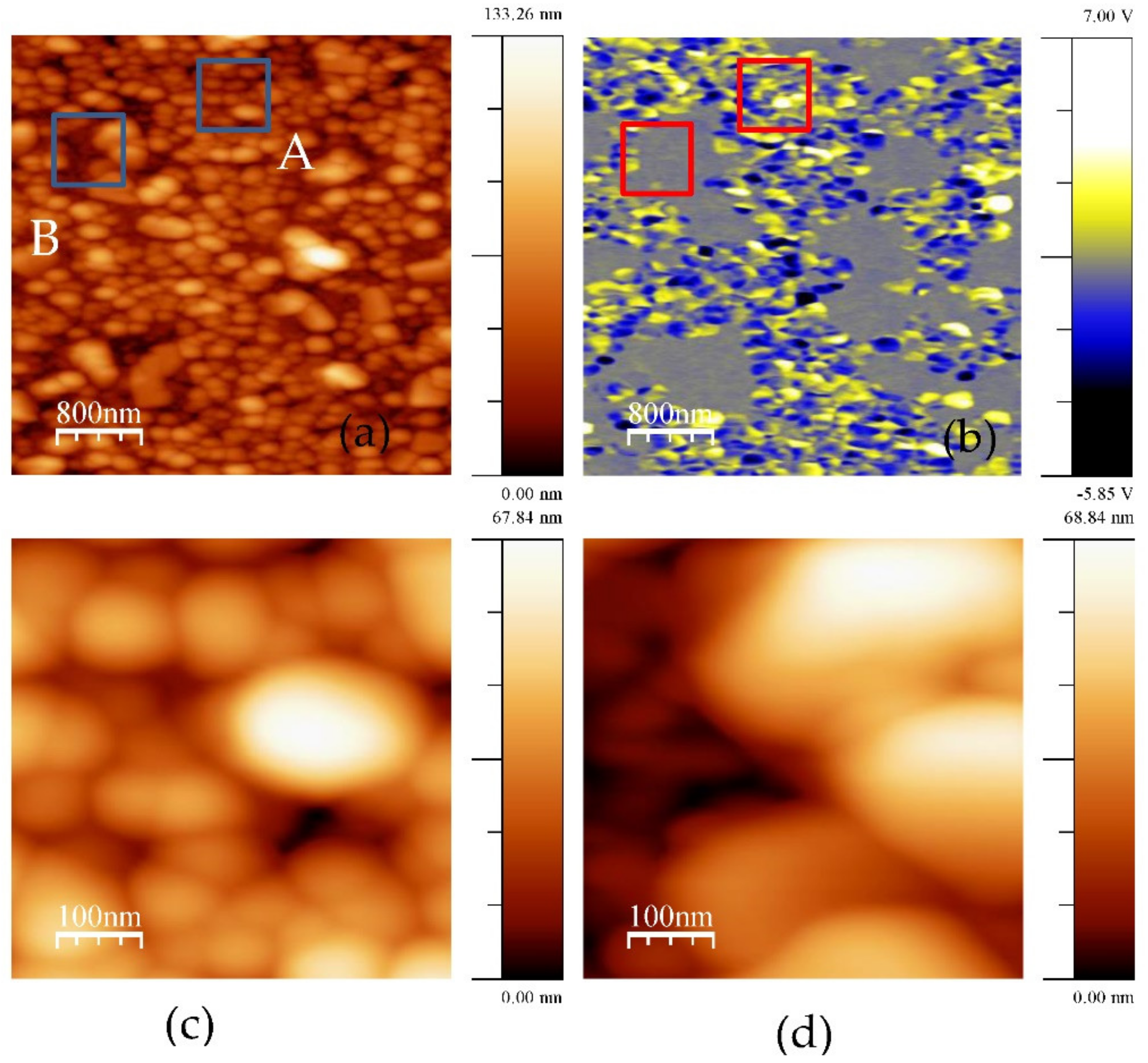
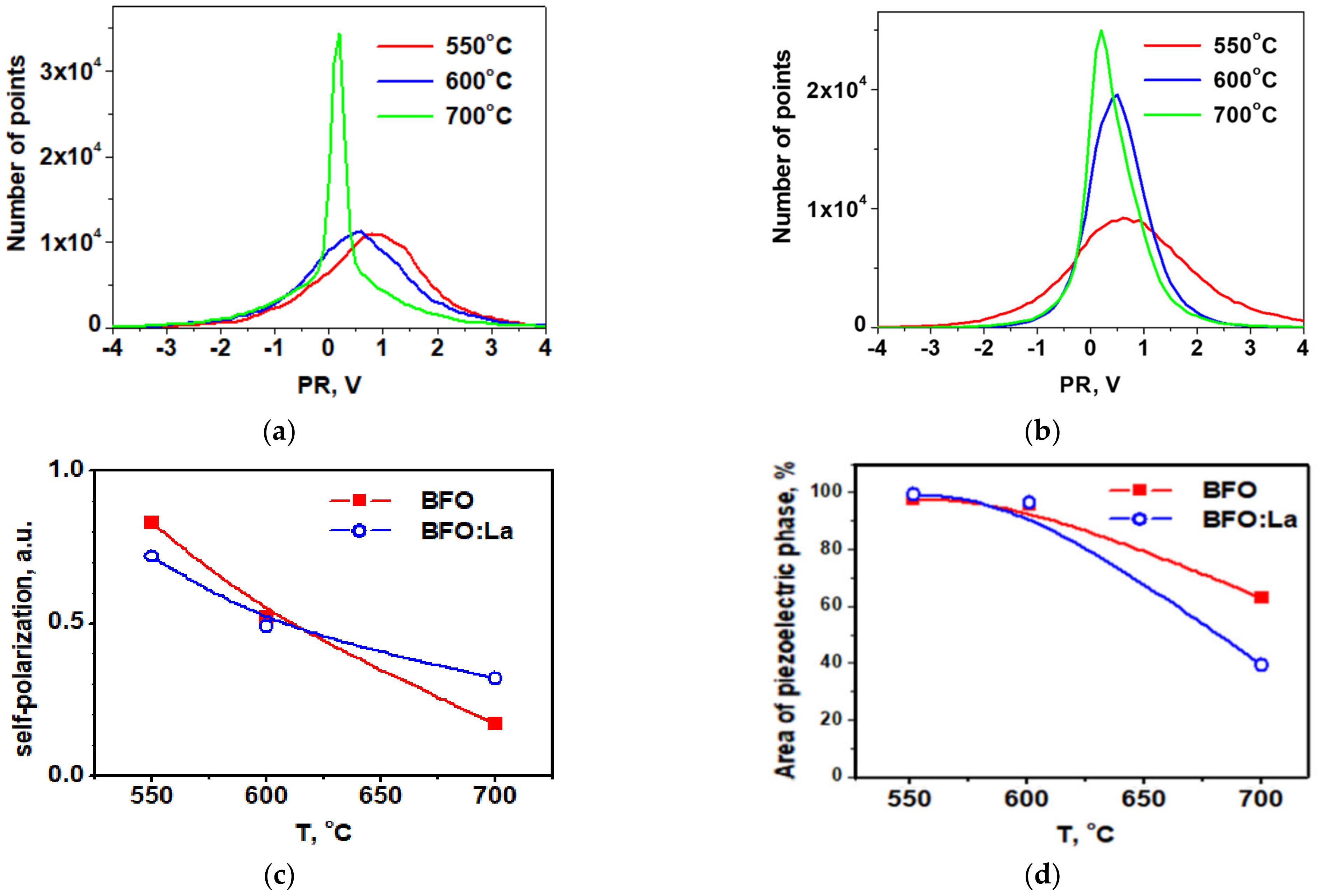
3. Results and Discussion
4. Conclusions
Author Contributions
Funding
Institutional Review Board Statement
Informed Consent Statement
Data Availability Statement
Conflicts of Interest
References
- Guo, E.J.; Herklotz, A.; Roth, R.; Christl, M.; Das, S.; Widdra, W.; Dörr, K. Tuning the switching time of BiFeO3 capacitors by electrodes’ conductivity. Appl. Phys. Lett. 2013, 103, 022905. [Google Scholar] [CrossRef]
- Guo, E.J.; Das, S.; Herklotz, A. Enhancement of switching speed of BiFeO3 capacitors by magnetic fields. APL Mater. 2014, 2, 096107. [Google Scholar] [CrossRef]
- Wu, J.; Fan, Z.; Xiao, D.; Zhu, J.; Wang, J. Multiferroic bismuth ferrite-based materials for multifunctional applications: Ceramic bulks, thin films and nanostructures. Prog. Mater. Sci. 2016, 84, 335–402. [Google Scholar] [CrossRef]
- Chen, Z.; Chen, Z.; Kuo, C.Y.; Tang, Y.; Dedon, L.R.; Li, Q.; Zhang, L.; Klewe, C.; Huang, Y.-L.; Prasad, B.; et al. Complex strain evolution of polar and magnetic order in multiferroic BiFeO3 thin films. Nat. Commun. 2018, 9, 3764. [Google Scholar] [CrossRef] [PubMed]
- Li, J.; Sha, N.; Zhao, Z. Effect of annealing atmosphere on the ferroelectric properties of inkjet printed BiFeO3 thin films. Appl. Surf. Sci. 2018, 454, 233–238. [Google Scholar] [CrossRef]
- Singh, D.; Tabari, T.; Ebadi, M.; Trochowski, M.; Yagci, M.B. Efficient synthesis of BiFeO3 by the microwave-assisted sol-gel method: “A”site influence on the photoelectrochemicalactivity of perovskites. Appl. Surf. Sci. 2019, 471, 1017–1027. [Google Scholar] [CrossRef]
- Machado, P.; Scigaj, M.; Gazquez, J.; Rueda, E.; Sanchez Díaz, A.; Fina, I.; Giber Roca, M.; Puig, T.; Obradors, X.; Campoy-Quiles, M.; et al. Band gap tuning of solution processed ferroelectric perovskite BiFe1−xCoxO3 thin films. Chem. Mater. 2019, 31, 947–954. [Google Scholar] [CrossRef]
- Karpinsky, D.V.; Troyanchuk, I.O.; Mantytskaya, O.S.; Khomchenko, V.A.; Kholkin, A.L. Structural stability and magnetic properties of Bi1−xLa(Pr)xFeO3 solid solutions. Solid State Commun. 2011, 151, 1686–1689. [Google Scholar] [CrossRef]
- Troyanchuk, I.O.; Karpinsky, D.V.; Bushinsky, M.V.; Khomchenko, V.A.; Kakazei, G.N.; Araujo, J.P.; Tovar, M.; Sikolenko, V.; Efimov, V.; Kholkin, A.L. Isothermal structural transitions, magnetization and large piezoelectric response in Bi1-xLaxFeO3 perovskites. Phys. Rev. B. 2011, 83, 054109–054115. [Google Scholar] [CrossRef]
- Singh Lotey, G.; Verma, N.K. Magnetoelectric coupling in multiferroic Tb-doped BiFeO3 nanoparticles. Mater. Lett. 2013, 111, 55–58. [Google Scholar] [CrossRef]
- Kim, W.-H.; Son, J.H. The effects of La substitution on ferroelectric domain structure and multiferroic properties of epitaxially grown BiFeO3 thin films. Appl. Phys. Lett. 2013, 103, 132907. [Google Scholar] [CrossRef]
- Pan, D.; Zhou, M.; Lu, Z.; Zhang, H.; Liu, J.-M.; Wang, G.-H.; Wan, J.-G. Local magnetoelectric effect in La-doped BiFeO3 multiferroic thin films revealed by magnetic-field-assisted scanning probe microscopy. Nanoscale Res. Lett. 2016, 11, 318. [Google Scholar] [CrossRef] [PubMed]
- Patel, R.; Sawadh, P. Tunable multiferroic properties of cerium doped bismuth ferrite. Nanosyst. Phys. Chem. Math. 2019, 10, 255–265. [Google Scholar] [CrossRef]
- Pradhan, S.K.; Roul, B.K. Effect of Gd doping on structural, electrical and magnetic properties of BiFeO3 electroceramic. J. Phys. Chem. Solids 2011, 72, 1180–1187. [Google Scholar] [CrossRef]
- Sinha, A.K.; Bhushan, B.; Jagannath Sharma, R.K.; Sen, S.; Mandal, B.P.; Meena, S.S.; Bhatt, P.; Prajapat, C.L.; Priyam, A.; Mishra, S.K.; et al. Enhanced dielectric, magnetic and optical properties of Cr-doped BiFeO3 multiferroic nanoparticles synthesized by sol-gel route. Results Phys. 2019, 13, 102299. [Google Scholar] [CrossRef]
- Mukherjee, S.; Gupta, R.; Garg, A.; Bansal, V.; Bhargava, S. Influence of Zr doping on the structure and ferroelectric properties of BiFeO3 thin films. J. Appl. Phys. 2010, 107, 123535. [Google Scholar] [CrossRef]
- Raghavender, A.T.; Hong, N.H. Effects of Mn doping on structural and magnetic properties of multiferroic BiFeO3 nanograins made by sol-gel method. J. Magn. 2011, 16, 19–22. [Google Scholar] [CrossRef]
- Zhang, C.; Song, Y.; Wang, M.; Yin, M.; Zhu, X.; Tian, L.; Wang, H.; Chen, X.; Fan, Z.; Lu, L.; et al. Efficient and flexible thin film amorphous silicon solar cells on nanotextured polymer substrate using sol-gel based nanoimprinting method. Adv. Funct. Mater. 2017, 27, 1604720. [Google Scholar] [CrossRef]
- Dominguez-Trujillo, C.; Peon, E.; Chicardia, E.; Perez, A.; Rodriguez-Ortiz, J.J.; Pavon, J.J.; Garcia-Couce, J.; Galvan, J.C.; Garcia-Moreno, F.; Torresa, Y. Sol-gel deposition of hydroxyapatite coatings on porous titanium for biomedical applications. Surf. Coat. Technol. 2018, 333, 158–162. [Google Scholar] [CrossRef]
- Ibrahim, I.; Dehghanghadikolaei, A.; Advincula, R.; Dean, D.; Luo, A.; Elahinia, M. Ceramic coating for delayed degradation of Mg-1.2Zn-0.5Ca-0.5Mn bone fixation and instrumentation. Thin Solid Film 2019, 687, 137456. [Google Scholar] [CrossRef]
- Sidsky, V.V.; Semchenko, A.V.; Rybakov, A.G.; Kolos, V.V.; Turtsevich, A.S.; Asadchyi, A.N.; Strek, W. La3+-doped SrBi2Ta2O9 thin films for FRAM synthesized by sol-gel method. J. Rare Earths 2014, 32, 277–281. [Google Scholar] [CrossRef]
- Perthuis, H.; Colomban, P. Well Densified NASICON Type Ceramics, Elaborated Using Sol-Gel Process and Sintering at Low Temperatures. Mater. Res. Bull. 1984, 19, 621–631. [Google Scholar] [CrossRef]
- Colomban, P. Gel Technology in Ceramics, Glass Ceramics and Ceramic-Ceramic Compositest. Ceram. Int. 1989, 15, 23–50. [Google Scholar] [CrossRef]
- Colomban, P. Chemical Preparation Routes and Lowering the Sintering Temperature of Ceramics. Ceramics 2020, 3, 312–339. [Google Scholar] [CrossRef]
- Balke, N.; Bdikin, I.K.; Kalinin, S.V.; Kholkin, A.L. Electromechanical imaging and spectroscopy of ferroelectric and piezoelectric materials: State-of-the-art and prospects for the future (feature article). J. Am. Ceram. Soc. 2009, 92, 1629–1647. [Google Scholar] [CrossRef]
- International Centre for Diffraction Data. Available online: http://www.icdd.com (accessed on 1 July 2020).
- Crystallographic Computing System for Standard and Modulated Structures. Available online: http://jana.fzu.cz/workshops/Jana2006%20Cookbook.pdf (accessed on 4 July 2020).
- Cullity, B.D.; Stock, S.R. Elements of X-ray Diffraction, 3rd ed.; Prentice-Hall: Upper Saddle River, NJ, USA, 2001. [Google Scholar]
- Open Source XRD Rietvield Refinement. Available online: http://profex.doebelin.org (accessed on 4 July 2020).
- Lin, Z.; Cai, W.; Jiang, W.; Fu, C.; Li, C.; Song, Y. Effects of annealing temperature on the microstructure, optical, ferroelectric and photovoltaic properties of BiFeO3 thin films prepared by sol-gel method. Ceram. Int. 2013, 39, 8729–8736. [Google Scholar] [CrossRef]
- Semchenko, A.V.; Khakhomov, S.A.; Sidsky, V.V.; Gaishun, V.E.; Kovalenko, D.L.; Strek, W.; Hreniak, D. Structural properties of BiFeO3 and Bi0,9La0,1FeO3 powders synthesized by sol-gel process. In Proceedings of the International Conference on Global Research and Education, Balatonfüred, Hungary, 4–7 September 2019; pp. 113–118. [Google Scholar]
- Rojac, T.; Bencan, A.; Malic, M.; Tutuncu, G.; Jones, J.L.; Daniels, J.E.; Damjanovic, D. BiFeO3 ceramics: Processing, electrical, and electromechanical properties. J. Am. Chem. Soc. 2014, 97, 1993–2011. [Google Scholar] [CrossRef]
- Tyholdt, F.; Jørgensen, S.; Fjellvåg, H.; Gunnæs, A.E. Synthesis of oriented BiFeO3 thin films by chemical solution deposition: Phase, texture, and microstructural development. J. Mater. Res. 2005, 20, 2127–2139. [Google Scholar] [CrossRef]
- Gwyddion—Free SPM (AFM, SNOM, NSOM, STM, MFM, …) Data Analysis Software. Available online: http://www.gwyddion.net (accessed on 1 September 2020).
- Bdikin, I.K.; Gracio, J.; Ayouchi, R.; Schwarz, R.; Kholkin, A.L. Local piezoelectric properties of ZnO thin films prepared by RF-plasma-assisted pulsed-laser deposition method. Nanotechnology 2010, 21, 235703. [Google Scholar] [CrossRef]
- Bhargav, K.K.; Ram, S.; Majumdera, S.B. Physics of the multi-functionality of lanthanum ferrite ceramics. J. Appl. Phys. 2014, 115, 204109. [Google Scholar] [CrossRef]
- Karpinsky, D.V.; Troyanchuk, I.O.; Tovar, M.; Sikolenko, V.; Efimov, V.; Kholkin, A.L. Evolution of crystal structure and ferroic properties of La-doped BiFeO3 ceramics near the rhombohedral-orthorhombic phase boundary. J. Alloys Compd. 2013, 555, 101–107. [Google Scholar] [CrossRef]
- Alikin, D.O.; Turygin, A.P.; Walker, J.; Bencan, A.; Malic, B.; Rojac, T.; Shur, V.Y.; Kholkin, A.L. The effect of phase assemblages, grain boundaries and domain structure on the local switching behavior of rare-earth modified bismuth ferrite ceramics. Acta Mater. 2017, 125, 265–273. [Google Scholar] [CrossRef]
- Huang, S.; Qiu, Y.; Yuan, S.L. Enhanced magnetization and electric polarization in Bi2Fe4O9 ceramics by magnetic field pre-sintering. Mater. Lett. 2015, 160, 323–326. [Google Scholar] [CrossRef]
- Zhang, Q.; Sando, D.; Nagarajan, V. Chemical route derived bismuth ferrite thin films and nanomaterials. J. Mater. Chem. C 2016, 4, 4092–4124. [Google Scholar] [CrossRef]
- Kholkin, A.L.; Brooks, K.G.; Taylor, D.V.; Hiboux, S.; Setter, N. Self-polarization effect in Pb(Zr,Ti)O3 thin films. Integr. Ferroelectr. 1998, 22, 525–533. [Google Scholar] [CrossRef]
- Melo, M.; Araújo, E.B.; Shvartsman, V.V.; Shur, V.; Kholkin, A. Thickness effect on the structure, grain size, and local piezoresponse of self-polarized lead lanthanum zirconate titanate thin films. J. Appl. Phys. 2016, 120, 054101. [Google Scholar] [CrossRef]
- Lima, E.C.; Araujo, E.B.; Bdikin, I.K.; Kholkin, A.L. The self-polarization effect in Pb(Zr0.5Ti0.5)O3 films with no preferred polarization. Mater. Res. Bull. 2012, 47, 3548. [Google Scholar] [CrossRef]
- Baek, S.H.; Park, J.; Kim, D.M.; Aksyuk, V.A.; Das, R.R.; Bu, S.D.; Felker, D.A.; Lettieri, J.; Vaithyanathan, V.; Bharadwaja, S.S.N.; et al. Giant Piezoelectricity on Si for hyperactive MEMS. Science 2011, 334, 958–961. [Google Scholar] [CrossRef] [PubMed]
- Clark, S.J.; Robertson, J. Band gap and Schottky barrier heights of multiferroic BiFeO3. Appl. Phys. Lett. 2007, 90, 132903. [Google Scholar] [CrossRef]
- Arnold, D.C. Composition-driven structural phase transitions in rare-earth-doped BiFeO3 ceramics: A review. IEEE Trans. Ultrason Ferroelectr. Freq. Control 2015, 62, 62–82. [Google Scholar] [CrossRef] [PubMed]


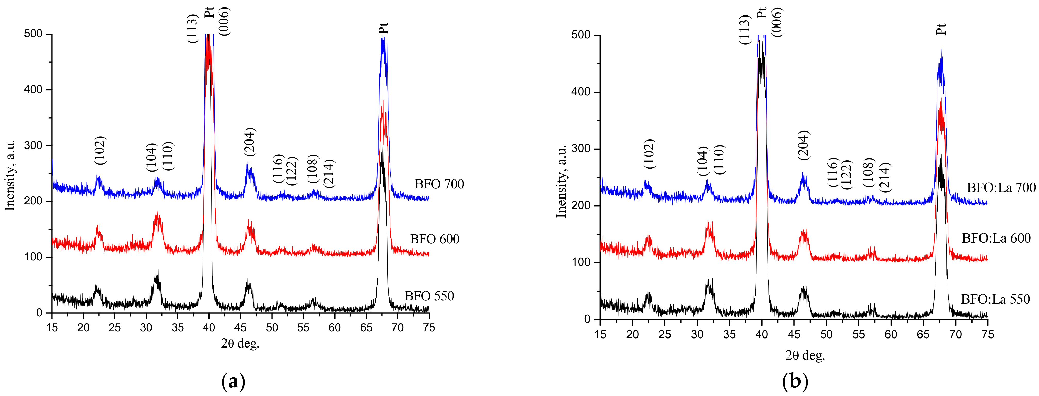
| Sample | Crystallization Temperature, °C | Perovskite Phase Content, % (±2%) | Crystallite Size, nm (±0.5 nm) |
|---|---|---|---|
| BFO | 550 | 70 | 9 |
| 600 | 94 | 5 | |
| 700 | 94 | 5 | |
| BLFO | 550 | 92 | 5 |
| 600 | 95 | 6 | |
| 700 | 97 | 6 |
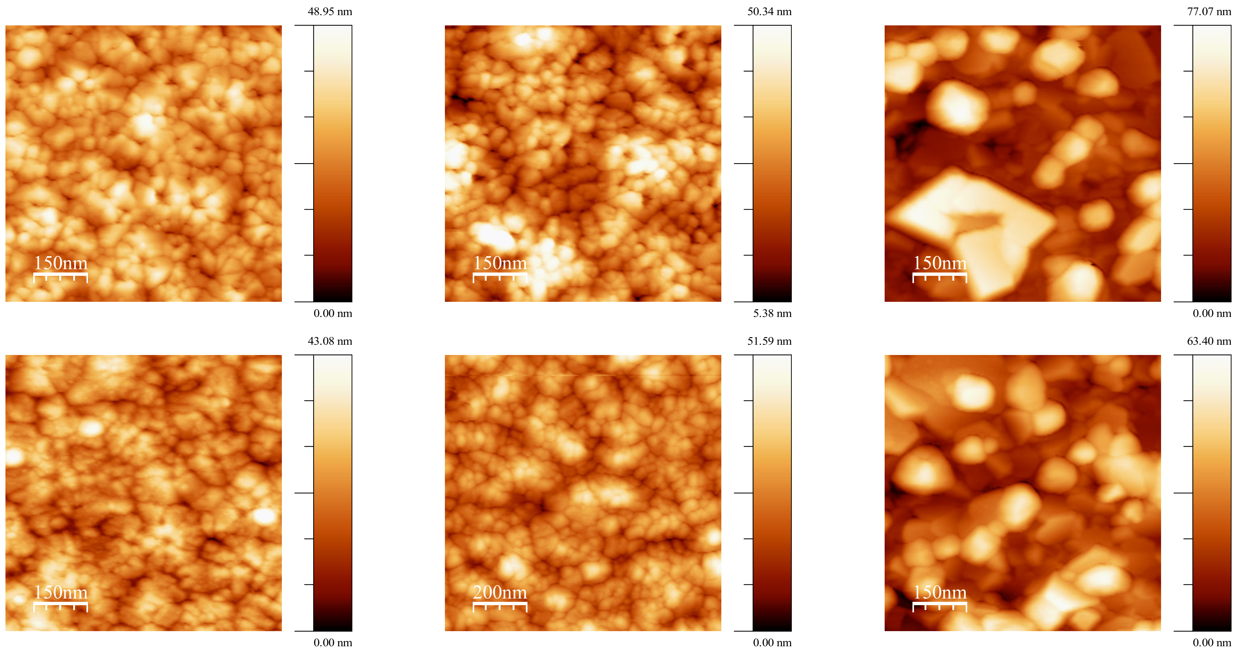
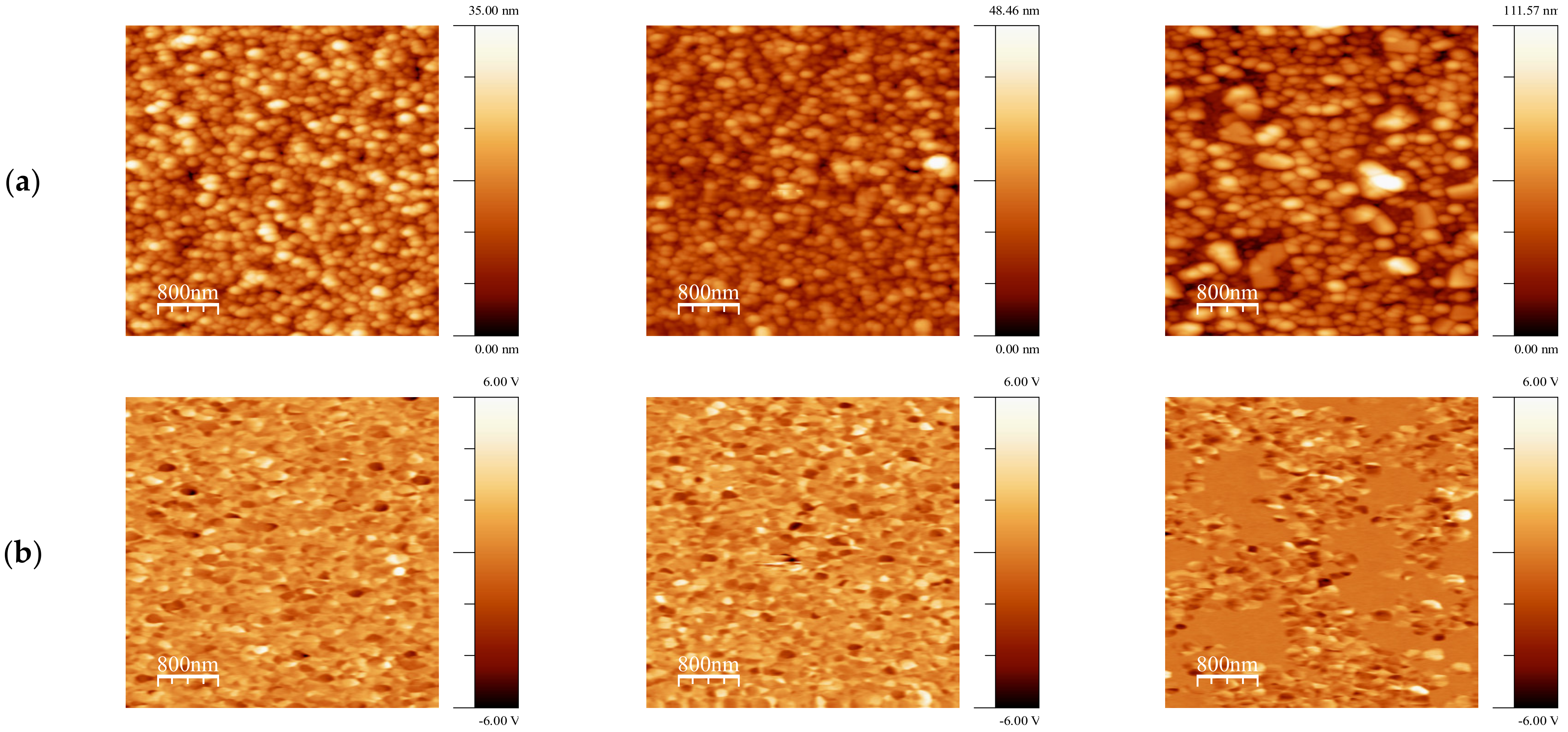
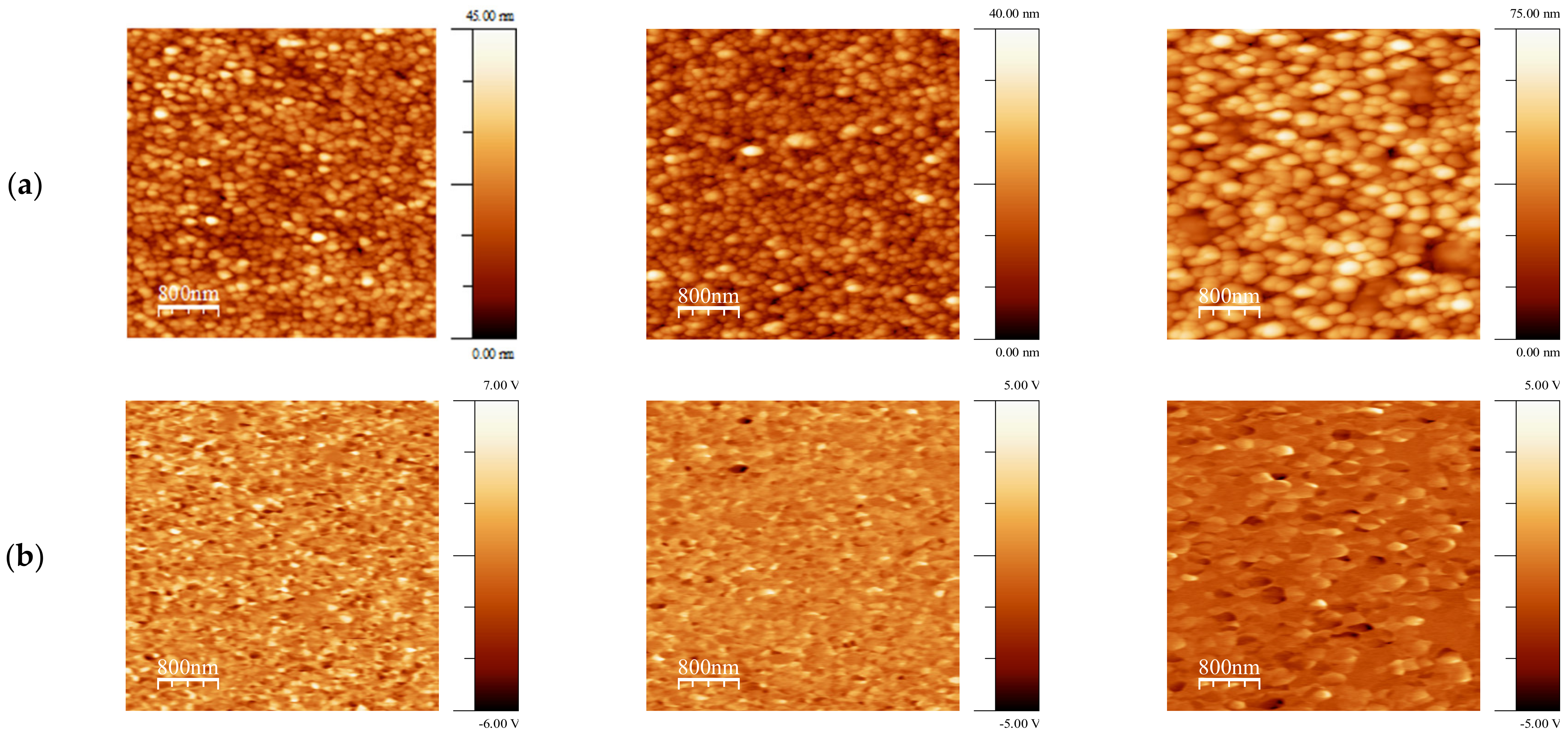
| Sample | Ra, nm | Average Grain Size, nm | Sample | Ra, nm | Average Grain Size, nm |
|---|---|---|---|---|---|
| BFO 550 °C | 8 | 90 | BLFO 550 °C | 4 | 85 |
| BFO 600 °C | 5 | 80 | BLFO 600 °C | 4 | 85 |
| BFO 700 °C | 10 | 100 | BLFO 700 °C | 9 | 135 |
Publisher’s Note: MDPI stays neutral with regard to jurisdictional claims in published maps and institutional affiliations. |
© 2021 by the authors. Licensee MDPI, Basel, Switzerland. This article is an open access article distributed under the terms and conditions of the Creative Commons Attribution (CC BY) license (https://creativecommons.org/licenses/by/4.0/).
Share and Cite
Semchenko, A.V.; Sidsky, V.V.; Bdikin, I.; Gaishun, V.E.; Kopyl, S.; Kovalenko, D.L.; Pakhomov, O.; Khakhomov, S.A.; Kholkin, A.L. Nanoscale Piezoelectric Properties and Phase Separation in Pure and La-Doped BiFeO3 Films Prepared by Sol–Gel Method. Materials 2021, 14, 1694. https://doi.org/10.3390/ma14071694
Semchenko AV, Sidsky VV, Bdikin I, Gaishun VE, Kopyl S, Kovalenko DL, Pakhomov O, Khakhomov SA, Kholkin AL. Nanoscale Piezoelectric Properties and Phase Separation in Pure and La-Doped BiFeO3 Films Prepared by Sol–Gel Method. Materials. 2021; 14(7):1694. https://doi.org/10.3390/ma14071694
Chicago/Turabian StyleSemchenko, Alina V., Vitaly V. Sidsky, Igor Bdikin, Vladimir E. Gaishun, Svitlana Kopyl, Dmitry L. Kovalenko, Oleg Pakhomov, Sergei A. Khakhomov, and Andrei L. Kholkin. 2021. "Nanoscale Piezoelectric Properties and Phase Separation in Pure and La-Doped BiFeO3 Films Prepared by Sol–Gel Method" Materials 14, no. 7: 1694. https://doi.org/10.3390/ma14071694
APA StyleSemchenko, A. V., Sidsky, V. V., Bdikin, I., Gaishun, V. E., Kopyl, S., Kovalenko, D. L., Pakhomov, O., Khakhomov, S. A., & Kholkin, A. L. (2021). Nanoscale Piezoelectric Properties and Phase Separation in Pure and La-Doped BiFeO3 Films Prepared by Sol–Gel Method. Materials, 14(7), 1694. https://doi.org/10.3390/ma14071694