
Formation of Li2CO3 Nanostructures for Lithium-Ion Battery Anode Application by Nanotransfer Printing

 and
and 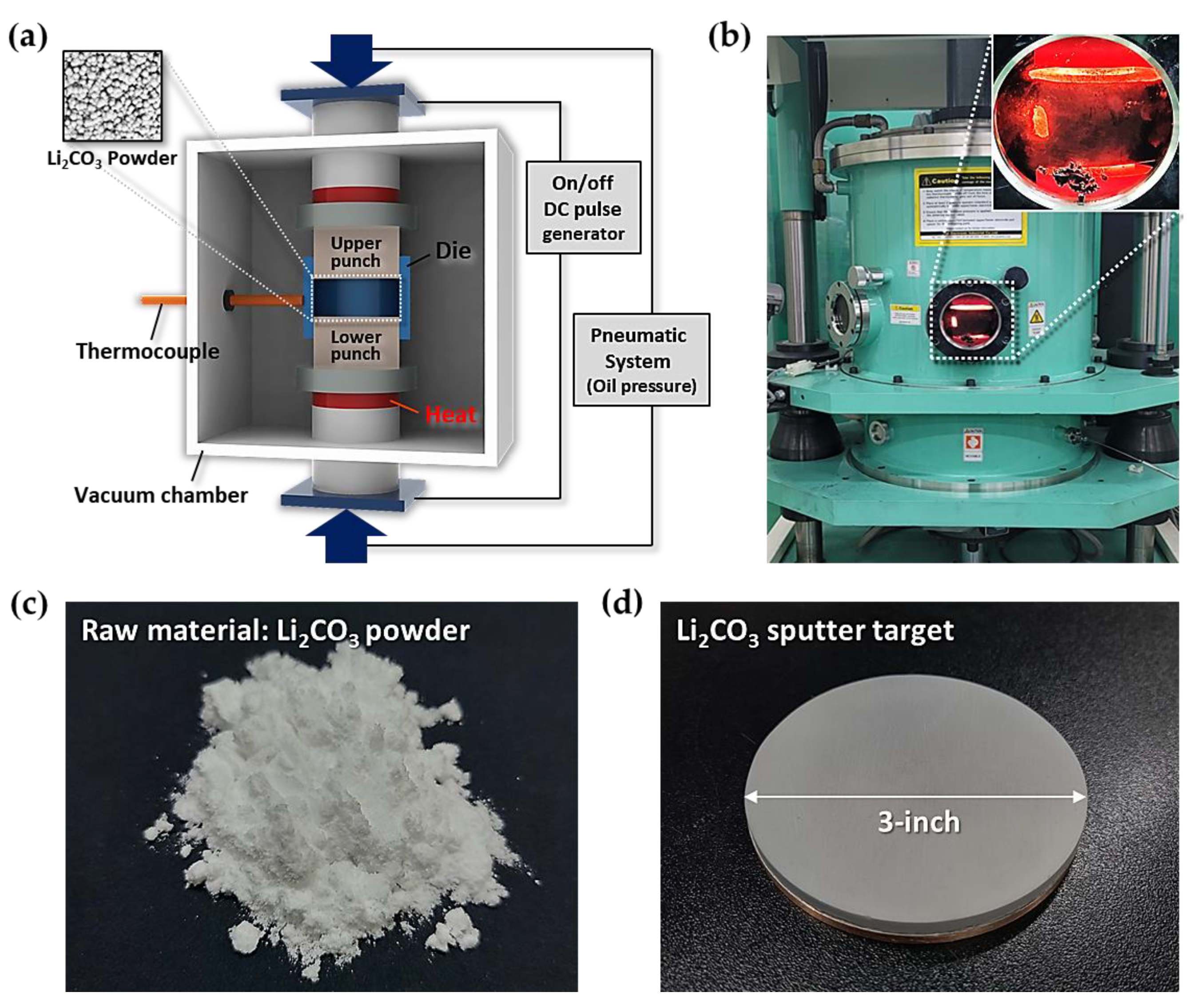
Abstract
1. Introduction
2. Materials and Methods
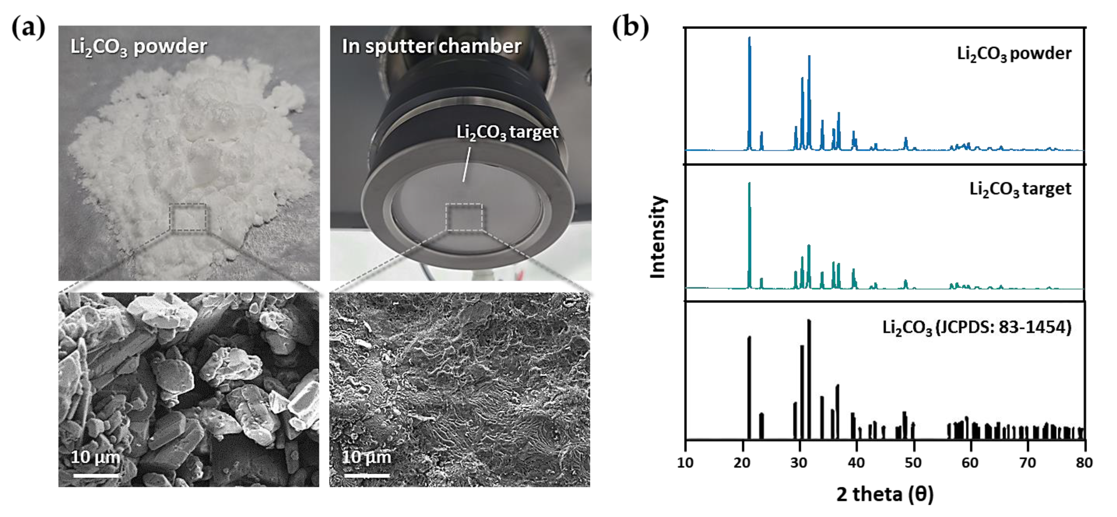
2.1. Fabrication of High-Density Li2CO3 Sputter Target
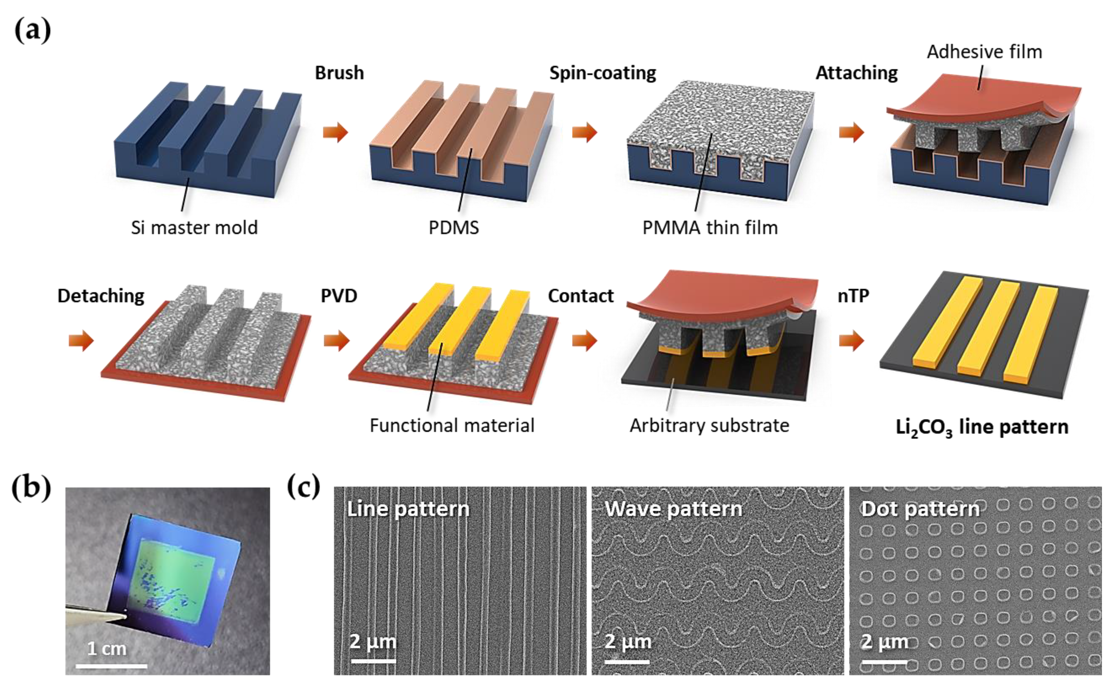
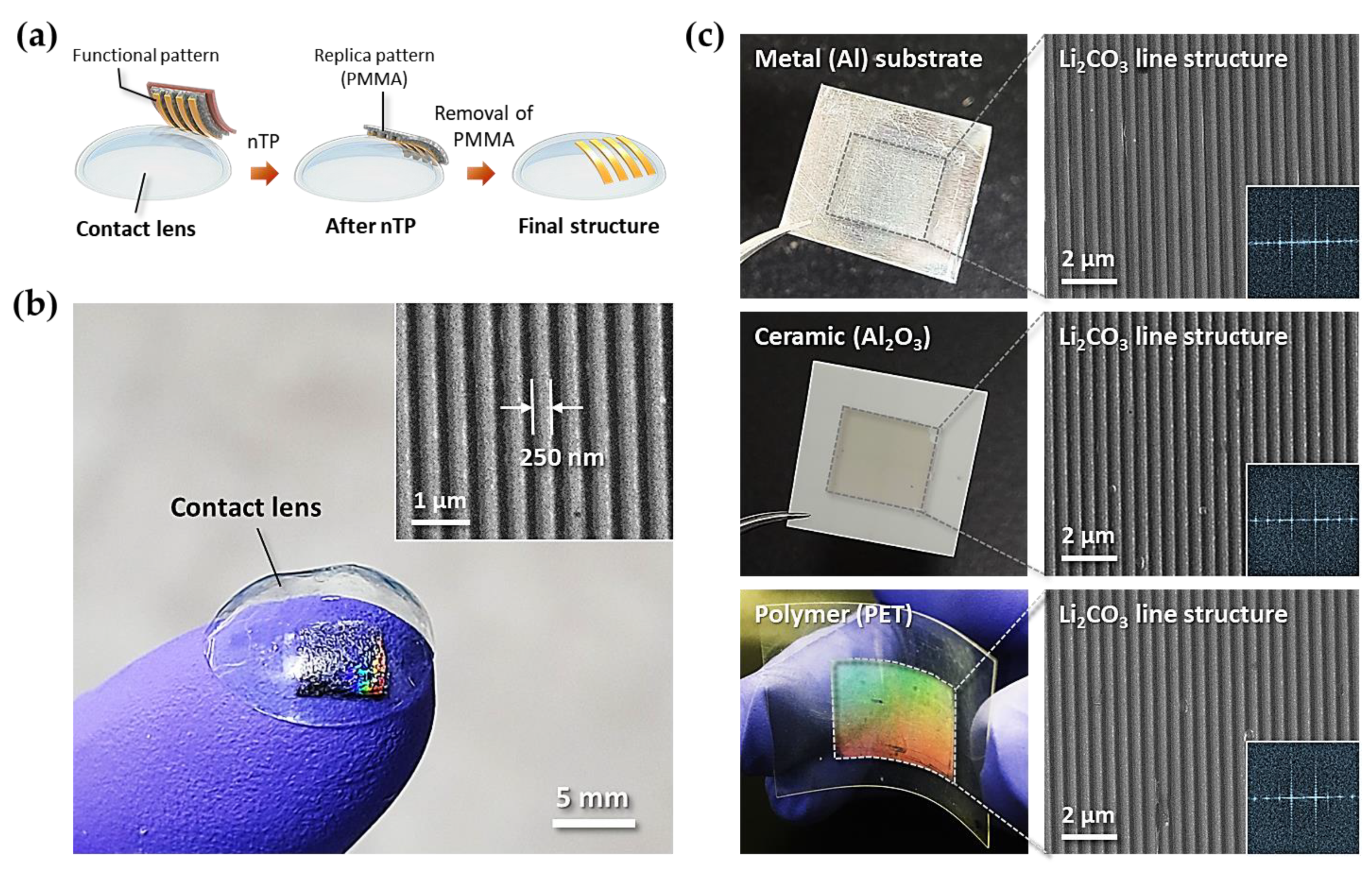
2.2. Procedure for the Formation of Li2CO3 Nanostructures via Nanotransfer Printing
3. Results and Discussion
4. Conclusions
Author Contributions
Funding
Institutional Review Board Statement
Informed Consent Statement
Data Availability Statement
Conflicts of Interest
References
- Sun, H.; Zhang, Y.; Zhang, J.; Sun, X.; Peng, H. Energy harvesting and storage in 1D devices. Nat. Rev. Mater. 2017, 2, 1–12. [Google Scholar] [CrossRef]
- Hu, Y.; Lin, L.; Zhang, Y.; Wang, Z.L. Replacing a battery by a nanogenerator with 20 V output. Adv. Mater. 2012, 24, 110–114. [Google Scholar] [CrossRef] [PubMed]
- Seung, W.; Gupta, M.K.; Lee, K.Y.; Shin, K.-S.; Lee, J.-H.; Kim, T.Y.; Kim, S.; Lin, J.; Kim, J.H.; Kim, S.-W. Nanopatterned textile-based wearable triboelectric nanogenerator. ACS Nano 2015, 9, 3501–3509. [Google Scholar] [CrossRef]
- Abtahi, A.; Johnson, S.; Park, S.M.; Luo, X.; Liang, Z.; Mei, J.; Graham, K.R. Designing π-conjugated polymer blends with improved thermoelectric power factors. J. Mater. Chem. A 2019, 7, 19774–19785. [Google Scholar] [CrossRef]
- Atanasov, V.; Lee, A.S.; Park, E.J.; Maurya, S.; Baca, E.D.; Fujimoto, C.; Hibbs, M.; Matanovic, I.; Kerres, J.; Kim, Y.S. Synergistically integrated phosphonated poly(pentafluorostyrene) for fuel cells. Nat. Mater. 2020, 20, 370–377. [Google Scholar] [CrossRef]
- Miyake, J.; Ogawa, Y.; Tanaka, T.; Ahn, J.; Oka, K.; Oyaizu, K.; Miyatake, K. Rechargeable proton exchange membrane fuel cell containing an intrinsic hydrogen storage polymer. Commun. Chem. 2020, 3, 138. [Google Scholar] [CrossRef]
- Nayak, P.K.; Mahesh, S.; Snaith, H.J.; Cahen, D. Photovoltaic solar cell technologies: Analysing the state of the art. Nat. Rev. Mater. 2019, 4, 269–285. [Google Scholar] [CrossRef]
- Park, S.M.; Abtahi, A.; Boehm, A.M.; Graham, K.R. Surface ligands for methylammonium lead iodide films: Surface coverage, energetics, and photovoltaic performance. ACS Energy Lett. 2020, 5, 799–806. [Google Scholar] [CrossRef]
- Hofmann, C.L.M.; Fischer, S.; Eriksen, E.H.; Bläsi, B.; Reitz, C.; Yazicioglu, D.; Howard, I.A.; Richards, B.S.; Goldschmidt, J.C. Experimental validation of a modeling framework for upconversion enhancement in 1D-photonic crystals. Nat. Commun. 2021, 12, 1–10. [Google Scholar] [CrossRef]
- Palacín, M.R. Recent advances in rechargeable battery materials: A chemist’s perspective. Chem. Soc. Rev. 2009, 38, 2565–2575. [Google Scholar] [CrossRef]
- Jiang, Z.; Li, J.; Yang, Y.; Mu, L.; Wei, C.; Yu, X.; Pianetta, P.; Zhao, K.; Cloetens, P.; Lin, F.; et al. Machine-learning-revealed statistics of the particle-carbon/binder detachment in lithium-ion battery cathodes. Nat. Commun. 2020, 11, 1–9. [Google Scholar] [CrossRef]
- Trahey, L.; Brushett, F.R.; Balsara, N.P.; Ceder, G.; Cheng, L.; Chiang, Y.-M.; Hahn, N.T.; Ingram, B.J.; Minteer, S.D.; Moore, J.S.; et al. Energy storage emerging: A perspective from the Joint Center for Energy Storage Research. Proc. Natl. Acad. Sci. USA 2020, 117, 12550–12557. [Google Scholar] [CrossRef]
- Chang, Z.; Li, C.; Wang, Y.; Chen, B.; Fu, L.; Zhu, Y.; Zhang, L.; Wu, Y.; Huang, W. A lithium ion battery using an aqueous electrolyte solution. Sci. Rep. 2016, 6, 28421. [Google Scholar] [CrossRef]
- Harper, G.; Sommerville, R.; Kendrick, E.; Driscoll, L.; Slater, P.; Stolkin, R.; Walton, A.; Christensen, P.; Heidrich, O.; Lambert, S.; et al. Recycling lithium-ion batteries from electric vehicles. Nature 2019, 575, 75–86. [Google Scholar] [CrossRef] [PubMed]
- Ahmadi, L.; Young, S.B.; Fowler, M.; Fraser, R.A.; Achachlouei, M.A. A cascaded life cycle: Reuse of electric vehicle lithium-ion battery packs in energy storage systems. Int. J. Life Cycle Assess. 2017, 22, 111–124. [Google Scholar] [CrossRef]
- Olivetti, E.A.; Ceder, G.; Gaustad, G.G.; Fu, X. Lithium-ion battery supply chain considerations: Analysis of potential bottlenecks in critical metals. Joule 2017, 1, 229–243. [Google Scholar] [CrossRef]
- Hannan, M.A.; Lipu, M.S.H.; Hussain, A.; Mohamed, A. A review of lithium-ion battery state of charge estimation and management system in electric vehicle applications: Challenges and recommendations. Renew. Sustain. Energy Rev. 2017, 78, 834–854. [Google Scholar] [CrossRef]
- Li, M.; Lu, J.; Chen, Z.; Amine, K. 30 Years of lithium-ion batteries. Adv. Mater. 2018, 30, e1800561. [Google Scholar] [CrossRef] [PubMed]
- Kittner, N.; Lill, F.; Kammen, D.M. Energy storage deployment and innovation for the clean energy transition. Nat. Energy 2017, 2, 1–6. [Google Scholar] [CrossRef]
- Xu, S.; Hessel, C.M.; Ren, H.; Yu, R.; Jin, Q.; Yang, M.; Zhao, H.; Wang, D. α-Fe2O3multi-shelled hollow microspheres for lithium ion battery anodes with superior capacity and charge retention. Energy Environ. Sci. 2014, 7, 632–637. [Google Scholar] [CrossRef]
- Zhao, Y.; Peng, L.; Ding, Y.; Yu, G. Amorphous silicon honeycombs as a binder/carbon-free, thin-film Li-ion battery anode. Chem. Commun. 2014, 50, 12959–12962. [Google Scholar] [CrossRef] [PubMed]
- Heiskanen, S.K.; Kim, J.; Lucht, B.L. Generation and evolution of the solid electrolyte interphase of lithium-ion batteries. Joule 2019, 3, 2322–2333. [Google Scholar] [CrossRef]
- Pender, J.P.; Jha, G.; Youn, D.H.; Ziegler, J.M.; Andoni, I.; Choi, E.J.; Heller, A.; Dunn, B.S.; Weiss, P.S.; Penner, R.M.; et al. Electrode degradation in lithium-ion batteries. ACS Nano 2020, 14, 1243–1295. [Google Scholar] [CrossRef]
- Komaba, S.; Watanabe, M.; Groult, H.; Kumagai, N. Alkali carbonate-coated graphite electrode for lithium-ion batteries. Carbon 2008, 46, 1184–1193. [Google Scholar] [CrossRef]
- Li, J.; Li, M.; Guo, C.; Zhang, L. Recent progress and challenges of micro-/nanostructured transition metal carbonate anodes for lithium ion batteries. Eur. J. Inorg. Chem. 2018, 41, 4508–4521. [Google Scholar] [CrossRef]
- Gao, Y.; Huang, C.; Hao, C.; Sun, S.; Zhang, L.; Zhang, C.; Duan, Z.; Wang, K.; Jin, Z.; Zhang, N.; et al. Lead halide perovskite nanostructures for dynamic color display. ACS Nano 2018, 12, 8847–8854. [Google Scholar] [CrossRef] [PubMed]
- Yao, Y.; Zhang, L.; Leydecker, T.; Samorì, P. Direct photolithography on molecular crystals for high performance organic optoelectronic devices. J. Am. Chem. Soc. 2018, 140, 6984–6990. [Google Scholar] [CrossRef] [PubMed]
- Cox, L.M.; Martinez, A.M.; Blevins, A.K.; Sowan, N.; Ding, Y.; Bowman, C.N. Nanoimprint lithography: Emergent materials and methods of actuation. Nano Today 2020, 31, 100838. [Google Scholar] [CrossRef]
- Chou, S.Y.; Krauss, P.R.; Renstrom, P.J. Imprint lithography with 25-nanometer resolution. Science 1996, 272, 85–87. [Google Scholar] [CrossRef]
- Torretti, F.; Sheil, J.; Schupp, R.; Basko, M.M.; Bayraktar, M.; Meijer, R.A.; Witte, S.; Ubachs, W.; Hoekstra, R.; Versolato, O.O.; et al. Prominent radiative contributions from multiply-excited states in laser-produced tin plasma for nanolithography. Nat. Commun. 2020, 11, 1–8. [Google Scholar] [CrossRef]
- Mojarad, N.; Gobrecht, J.; Ekinci, Y. Beyond EUV lithography: A comparative study of efficient photoresists’ performance. Sci. Rep. 2015, 5, srep09235. [Google Scholar] [CrossRef]
- Park, W.I.; Jung, Y.K.; Kim, Y.; Shin, W.H.; Choi, Y.J.; Park, T.W.; Shin, J.H.; Jeong, Y.H.; Cho, J.H.; Shin, H.; et al. Individual confinement of block copolymer microdomains in nanoscale crossbar templates. Adv. Funct. Mater. 2018, 29, 1805795. [Google Scholar] [CrossRef]
- Jung, H.; Shin, W.H.; Park, T.W.; Choi, Y.J.; Yoon, Y.J.; Park, S.H.; Lim, J.-H.; Kwon, J.-D.; Lee, J.W.; Kwon, S.-H.; et al. Hierarchical multi-level block copolymer patterns by multiple self-assembly. Nanoscale 2019, 11, 8433–8441. [Google Scholar] [CrossRef]
- Jung, D.S.; Bang, J.; Park, T.W.; Lee, S.H.; Jung, Y.K.; Byun, M.; Cho, Y.R.; Kim, K.H.; Seong, G.H.; Park, W.I. Pattern formation of metal–oxide hybrid nanostructures via the self-assembly of di-block copolymer blends. Nanoscale 2019, 11, 18559–18567. [Google Scholar] [CrossRef] [PubMed]
- Onses, M.S.; Song, C.; Williamson, L.; Sutanto, E.; Ferreira, P.M.; Alleyne, A.G.; Nealey, P.F.; Ahn, H.; Rogers, J.A. Hierarchical patterns of three-dimensional block-copolymer films formed by electrohydrodynamic jet printing and self-assembly. Nat. Nanotechnol. 2013, 8, 667–675. [Google Scholar] [CrossRef] [PubMed]
- Pham, T.A.; Nguyen, T.K.; Vadivelu, R.K.; Dinh, T.; Qamar, A.; Yadav, S.; Yamauchi, Y.; Rogers, J.A.; Nguyen, N.T.; Phan, H.P. A versatile sacrificial layer for transfer printing of wide bandgap materials for implantable and stretchable bioelectronics. Adv. Funct. Mater. 2020, 30, 2004655. [Google Scholar] [CrossRef]
- Chanda, D.; Shigeta, K.; Gupta, S.; Cain, T.; Carlson, A.; Mihi, A.; Baca, A.J.; Bogart, G.R.; Braun, P.V.; Rogers, J.A. Large-area flexible 3D optical negative index metamaterial formed by nanotransfer printing. Nat. Nanotechnol. 2011, 6, 402–407. [Google Scholar] [CrossRef] [PubMed]
- Cho, S.H.; Baek, K.M.; Han, H.J.; Kim, M.; Park, H.; Jung, Y.S. Selective, quantitative, and multiplexed surface-enhanced raman spectroscopy using aptamer-functionalized monolithic plasmonic nanogrids derived from cross-point nano-welding. Adv. Funct. Mater. 2020, 30, 2000612. [Google Scholar] [CrossRef]
- Choi, M.K.; Yang, J.; Kang, K.; Kim, D.C.; Choi, C.; Park, C.; Kim, S.J.; Chae, S.I.; Kim, T.-H.; Kim, J.H.; et al. Wearable red–green–blue quantum dot light-emitting diode array using high-resolution intaglio transfer printing. Nat. Commun. 2015, 6, 7149. [Google Scholar] [CrossRef]
- Ahn, J.-H.; Kim, H.-S.; Lee, K.J.; Jeon, S.; Kang, S.J.; Sun, Y.; Nuzzo, R.G.; Rogers, J.A. Heterogeneous three-dimensional electronics by use of printed semiconductor nanomaterials. Science 2006, 314, 1754–1757. [Google Scholar] [CrossRef] [PubMed]
- Zaumseil, J.; Meitl, M.A.; Hsu, J.W.P.; Acharya, B.R.; Baldwin, K.W.; Loo, Y.-L.; Rogers, J.A. Three-dimensional and multilayer nanostructures formed by nanotransfer printing. Nano Lett. 2003, 3, 1223–1227. [Google Scholar] [CrossRef]
- Meitl, M.A.; Zhu, Z.-T.; Kumar, V.; Lee, K.J.; Feng, X.; Huang, Y.Y.; Adesida, I.; Nuzzo, R.G.; Rogers, J.A. Transfer printing by kinetic control of adhesion to an elastomeric stamp. Nat. Mater. 2006, 5, 33–38. [Google Scholar] [CrossRef]
- Park, T.W.; Byun, M.; Jung, H.; Lee, G.R.; Park, J.H.; Jang, H.-I.; Lee, J.W.; Kwon, S.H.; Hong, S.; Lee, J.-H.; et al. Thermally assisted nanotransfer printing with sub–20-nm resolution and 8-inch wafer scalability. Sci. Adv. 2020, 6, eabb6462. [Google Scholar] [CrossRef] [PubMed]


Publisher’s Note: MDPI stays neutral with regard to jurisdictional claims in published maps and institutional affiliations. |
© 2021 by the authors. Licensee MDPI, Basel, Switzerland. This article is an open access article distributed under the terms and conditions of the Creative Commons Attribution (CC BY) license (http://creativecommons.org/licenses/by/4.0/).
Share and Cite
Park, T.W.; Kang, Y.L.; Lee, S.H.; No, G.W.; Park, E.-S.; Park, C.; Lee, J.; Park, W.I. Formation of Li2CO3 Nanostructures for Lithium-Ion Battery Anode Application by Nanotransfer Printing. Materials 2021, 14, 1585. https://doi.org/10.3390/ma14071585
Park TW, Kang YL, Lee SH, No GW, Park E-S, Park C, Lee J, Park WI. Formation of Li2CO3 Nanostructures for Lithium-Ion Battery Anode Application by Nanotransfer Printing. Materials. 2021; 14(7):1585. https://doi.org/10.3390/ma14071585
Chicago/Turabian StylePark, Tae Wan, Young Lim Kang, Sang Hyeon Lee, Gu Won No, Eun-Soo Park, Chan Park, Junghoon Lee, and Woon Ik Park. 2021. "Formation of Li2CO3 Nanostructures for Lithium-Ion Battery Anode Application by Nanotransfer Printing" Materials 14, no. 7: 1585. https://doi.org/10.3390/ma14071585
APA StylePark, T. W., Kang, Y. L., Lee, S. H., No, G. W., Park, E.-S., Park, C., Lee, J., & Park, W. I. (2021). Formation of Li2CO3 Nanostructures for Lithium-Ion Battery Anode Application by Nanotransfer Printing. Materials, 14(7), 1585. https://doi.org/10.3390/ma14071585