
Ultrahigh Temperature Flash Sintering of Binder-Less Tungsten Carbide within 6 s


 , ,
, , 
 and
and 
Abstract
1. Introduction
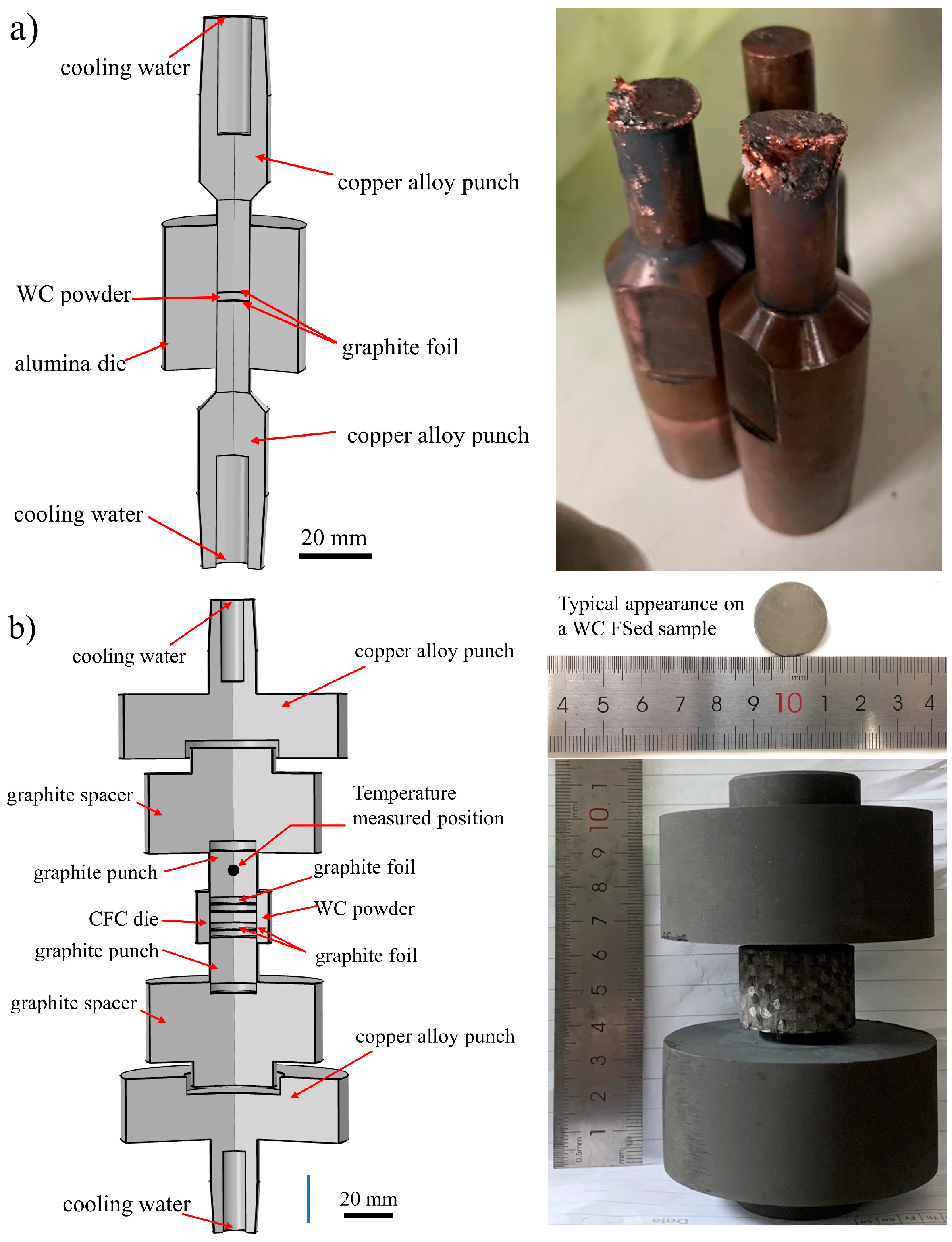
2. Experimental Section
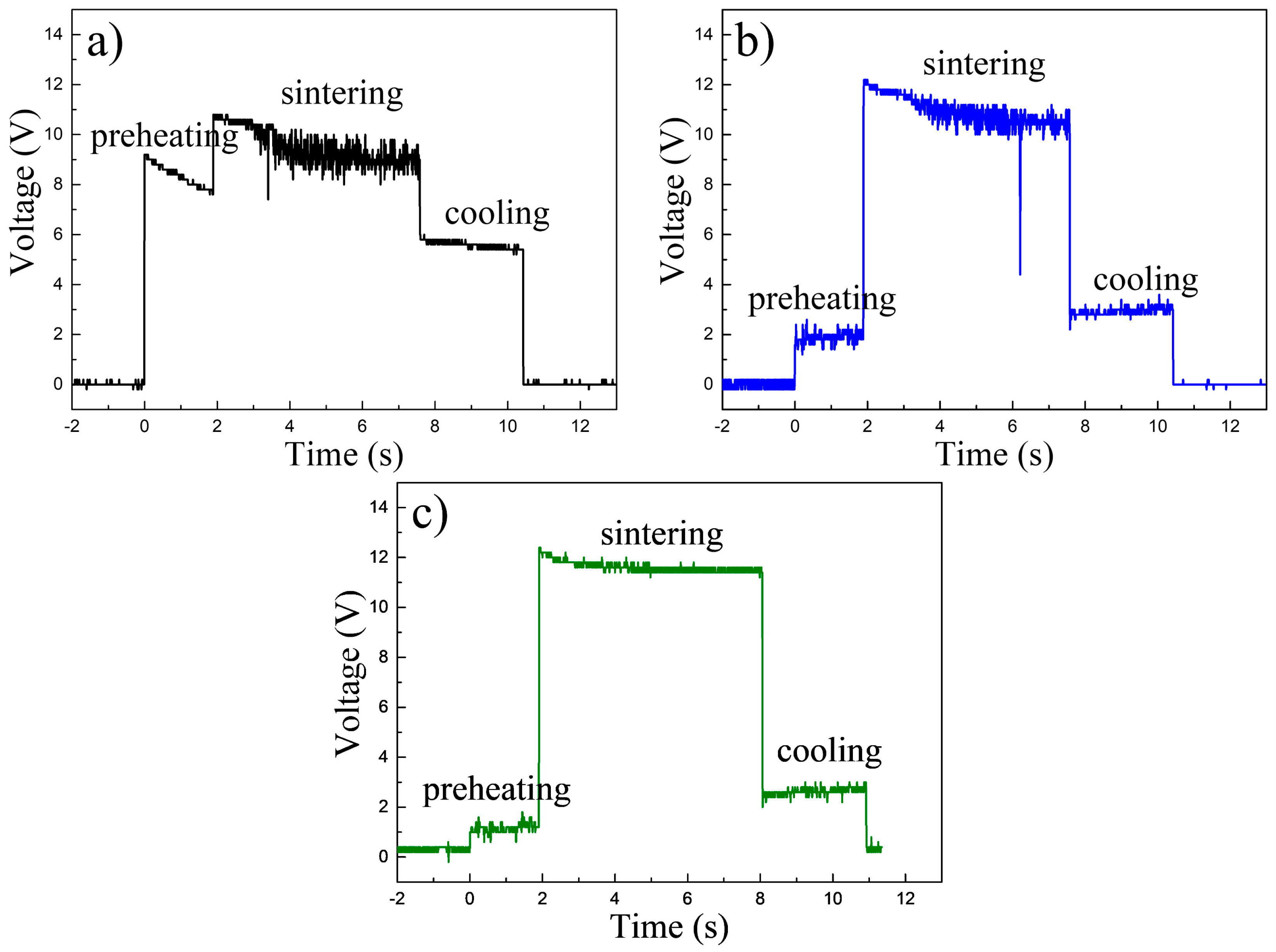
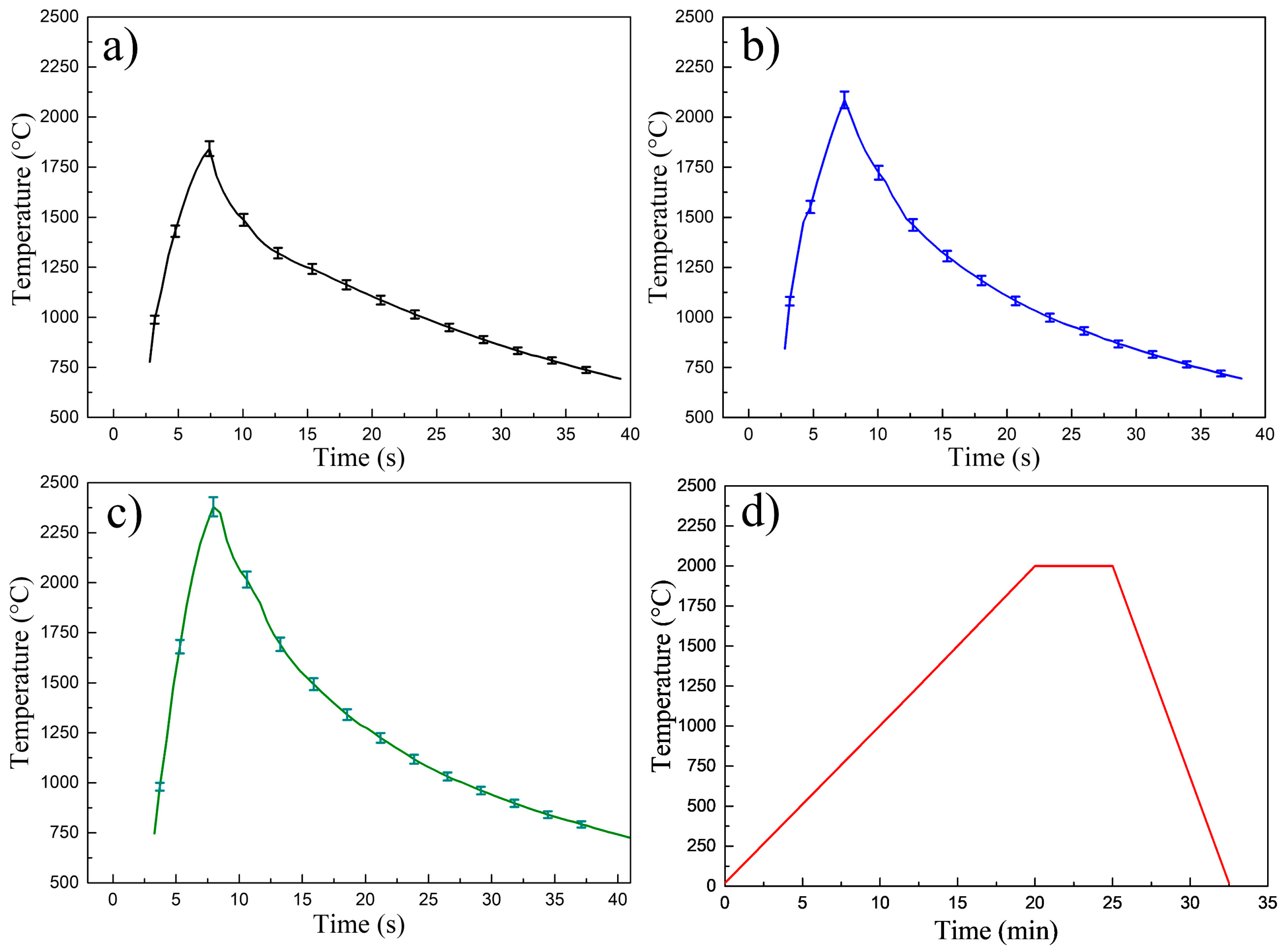
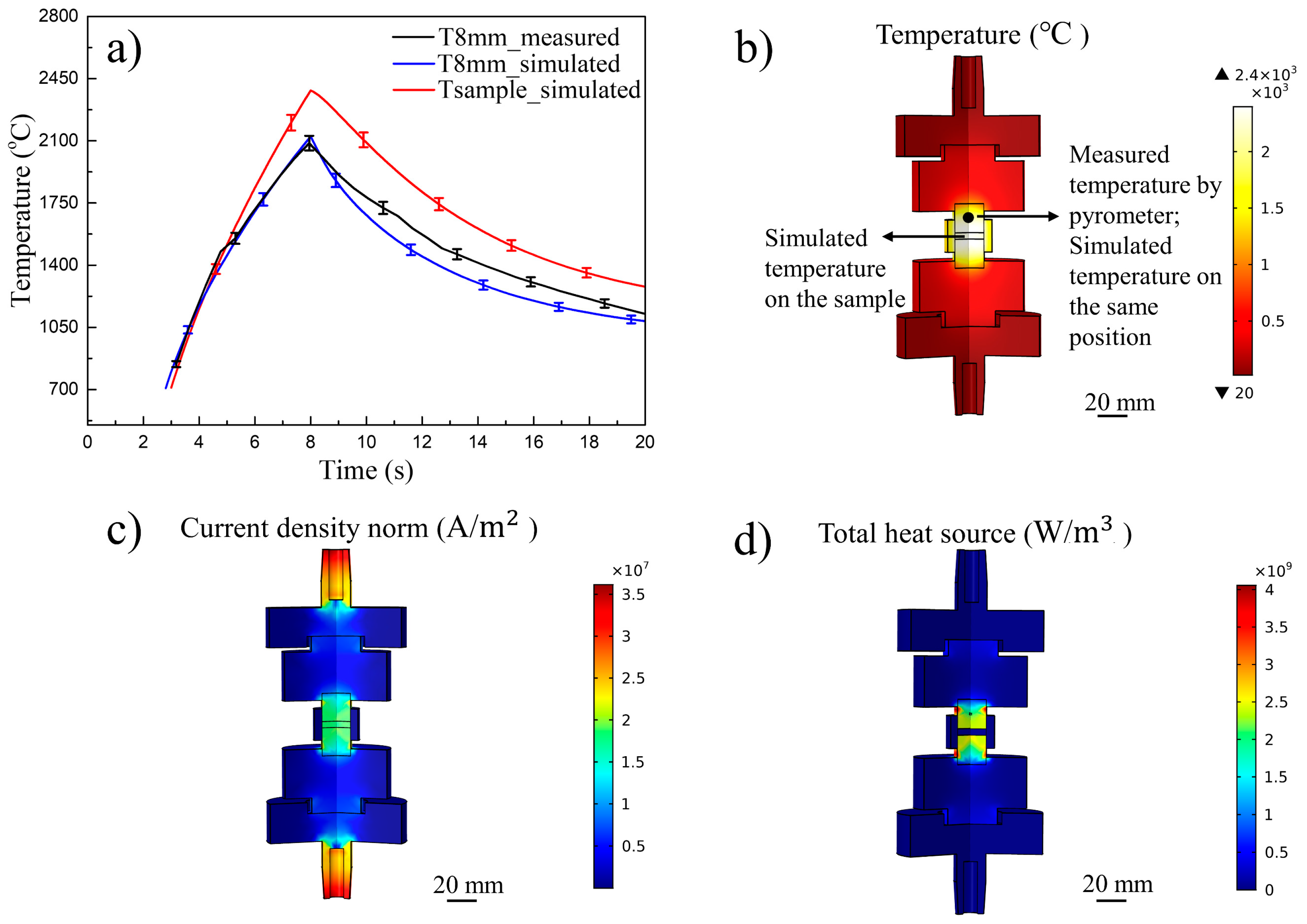
3. Results and Discussion
4. Conclusions
Supplementary Materials
Author Contributions
Funding
Institutional Review Board Statement
Informed Consent Statement
Data Availability Statement
Conflicts of Interest
References
- Cherrington, M.; Claypole, T.C.; Deganello, D.; Mabbett, I.; Watson, T.; Worsley, D. Ultrafast near-infrared sintering of a slot-die coated nano-silver conducting ink. J. Mater. Chem. 2011, 21, 7562–7564. [Google Scholar] [CrossRef]
- Olevsky, E.A.; Dudina, D.V. Field-Assisted Sintering; Springer International Publishing: Cham, Switzerland, 2018; ISBN 978-3-319-76031-5. [Google Scholar]
- Rahaman, M.N. Ceramic Processing and Sintering; Marcel Dekker: New York, NY, USA, 2017. [Google Scholar]
- Biesuz, M.; Grasso, S.; Sglavo, V.M. What’s new in ceramics sintering? A short report on the latest trends and future prospects. Curr. Opin. Solid State Mater. Sci. 2020, 24, 100868. [Google Scholar] [CrossRef]
- Grasso, S.; Sakka, Y.; Maizza, G. Electric current activated/assisted sintering (ECAS): A review of patents 1906–2008. Sci. Technol. Adv. Mater. 2009, 10, 053001. [Google Scholar] [CrossRef] [PubMed]
- Biesuz, M.; Saunders, T.; Ke, D.; Reece, M.J.; Hu, C.; Grasso, S. A review of electromagnetic processing of materials (EPM): Heating, sintering, joining and forming. J. Mater. Sci. Technol. 2021, 69, 239–272. [Google Scholar] [CrossRef]
- Biesuz, M.; Sglavo, V.M. Beyond flash sintering: How the flash event could change ceramics and glass processing. Scr. Mater. 2020, 187, 49–56. [Google Scholar] [CrossRef]
- Reeja-Jayan, B.; Luo, J. Far-from-equilibrium effects of electric and electromagnetic fields in ceramics synthesis and processing. MRS Bull. 2021, 46, 26–35. [Google Scholar] [CrossRef]
- Guillon, O.; De Souza, R.A.; Mishra, T.P.; Rheinheimer, W. Electric-field-assisted processing of ceramics: Nonthermal effects and related mechanisms. MRS Bull. 2021, 46, 52–58. [Google Scholar] [CrossRef]
- Cologna, M.; Rashkova, B.; Raj, R. Flash sintering of nanograin zirconia in <5 s at 850 °C. J. Am. Ceram. Soc. 2010, 93, 3556–3559. [Google Scholar] [CrossRef]
- Todd, R.I.; Zapata-Solvas, E.; Bonilla, R.S.; Sneddon, T.; Wilshaw, P.R. Electrical characteristics of flash sintering: Thermal runaway of Joule heating. J. Eur. Ceram. Soc. 2015, 35, 1865–1877. [Google Scholar] [CrossRef]
- Biesuz, M.; Sglavo, V.M. Microstructural temperature gradient-driven diffusion: Possible densification mechanism for flash sintering of zirconia? Ceram. Int. 2019, 45, 1227–1236. [Google Scholar] [CrossRef]
- Chaim, R. On the kinetics of liquid-assisted densification during flash sintering of ceramic nanoparticles. Scr. Mater. 2019, 158, 88–90. [Google Scholar] [CrossRef]
- Serrazina, R.; Dean, J.S.; Reaney, I.M.; Senos, A.M.O.R.; Vilarinho, P.M.; Pereira, L. Mechanism of densification in low-temperature flash sintered lead free potassium sodium. J. Mater. Chem. C 2019, 7, 14334–14341. [Google Scholar] [CrossRef]
- Ji, W.; Parker, B.; Falco, S.; Zhang, J.Y.; Fu, Z.Y.; Todd, R.I. Ultra-fast firing: Effect of heating rate on sintering of 3YSZ, with and without an electric field. J. Eur. Ceram. Soc. 2017, 37, 2547–2551. [Google Scholar] [CrossRef]
- Zhang, Y.; Nie, J.; Chan, J.M.; Luo, J. Probing the densification mechanisms during flash sintering of ZnO. Acta Mater. 2017, 125, 465–475. [Google Scholar] [CrossRef]
- Ren, K.; Wang, Q.; Lian, Y.; Wang, Y. Densification kinetics of flash sintered 3mol% Y2O3 stabilized zirconia. J. Alloys Compd. 2018, 747, 1073–1077. [Google Scholar] [CrossRef]
- Biesuz, M.; Sglavo, V.M. Electric forces effect on field-assisted sintering. J. Eur. Ceram. Soc. 2020, 40, 6259–6265. [Google Scholar] [CrossRef]
- Biesuz, M.; Pinter, L.; Saunders, T.; Reece, M.; Binner, J.; Sglavo, V.M.; Grasso, S. Investigation of Electrochemical, Optical and Thermal Effects during Flash Sintering of 8YSZ. Materials 2018, 11, 1214. [Google Scholar] [CrossRef]
- Liu, D.; Cao, Y.; Liu, J.; Gao, Y.; Wang, Y. Effect of oxygen partial pressure on temperature for onset of flash sintering 3YSZ. J. Eur. Ceram. Soc. 2018, 38, 817–820. [Google Scholar] [CrossRef]
- Jha, S.K.; Charalambous, H.; Wang, H.; Phuah, X.L.; Mead, C.; Okasinski, J.; Wang, H.; Tsakalakos, T. In-situ observation of oxygen mobility and abnormal lattice expansion in ceria during flash sintering. Ceram. Int. 2018, 44, 15362–15369. [Google Scholar] [CrossRef]
- Muccillo, R.; Muccillo, E.N.S. Electric field-assisted flash sintering of tin dioxide. J. Eur. Ceram. Soc. 2014, 34, 915–923. [Google Scholar] [CrossRef]
- Karakuscu, A.; Cologna, M.; Yarotski, D.; Won, J.; Francis, J.S.C.; Raj, R.; Uberuaga, B.P. Defect structure of flash-sintered strontium titanate. J. Am. Ceram. Soc. 2012, 95, 2531–2536. [Google Scholar] [CrossRef]
- Zhang, Y.; Luo, J. Promoting the flash sintering of ZnO in reduced atmospheres to achieve nearly full densities at furnace temperatures of <120 °C. Scr. Mater. 2015, 106, 26–29. [Google Scholar] [CrossRef]
- Gaur, A.; Mohiddon, M.A.; Sglavo, V.M. Phenomenological understanding of flash sintering in MnCo2O4. J. Eur. Ceram. Soc. 2018, 38, 4543–4552. [Google Scholar] [CrossRef]
- Prette, A.L.G.; Cologna, M.; Sglavo, V.; Raj, R. Flash-sintering of Co2MnO4 spinel for solid oxide fuel cell applications. J. Power Sources 2011, 196, 2061–2065. [Google Scholar] [CrossRef]
- Akbari-Fakhrabadi, A.; Mangalaraja, R.V.; Sanhueza, F.A.; Avila, R.E.; Ananthakumar, S.; Chan, S.H. Nanostructured Gd-CeO2 electrolyte for solid oxide fuel cell by aqueous tape casting. J. Power Sources 2012, 218, 307–312. [Google Scholar] [CrossRef]
- Spiridigliozzi, L.; Biesuz, M.; Dell’Agli, G.; Di Bartolomeo, E.; Zurlo, F.; Sglavo, V.M. Microstructural and electrical investigation of flash-sintered Gd/Sm-doped ceria. J. Mater. Sci. 2017, 52, 7479–7488. [Google Scholar] [CrossRef]
- Caliman, L.B.; Bouchet, R.; Gouvea, D.; Soudant, P.; Steil, M.C. Flash sintering of ionic conductors: The need of a reversible electrochemical reaction. J. Eur. Ceram. Soc. 2016, 36, 1253–1260. [Google Scholar] [CrossRef]
- Ojaimi, C.L.; Ferreira, J.A.; Chinelatto, A.L.; Chinelatto, A.S.A.; Pallone, E. Microstructural analysis of ZrO2/Al2O3 composite: Flash and conventional sintering. Ceram. Int. 2020, 46, 2473–2480. [Google Scholar] [CrossRef]
- Marinha, D.; Belmonte, M. Mixed-ionic and electronic conduction and stability of YSZ-graphene composites. J. Eur. Ceram. Soc. 2019, 39, 389–395. [Google Scholar] [CrossRef]
- Guan, L.; Li, J.; Song, X.; Bao, J.; Jiang, T. Graphite assisted flash sintering of Sm2O3 doped CeO2 ceramics at the onset temperature of 25 °C. Scr. Mater. 2019, 159, 72–75. [Google Scholar] [CrossRef]
- Muccillo, R.; Ferlauto, A.S.; Muccillo, E.N.S. Flash Sintering Samaria-Doped Ceria–Carbon Nanotube Composites. Ceramics 2019, 2, 64–73. [Google Scholar] [CrossRef]
- Manière, C.; Lee, G.; Olevsky, E.A. All-Materials-Inclusive Flash Spark Plasma Sintering. Sci. Rep. 2017, 7, 15071. [Google Scholar] [CrossRef]
- Grasso, S.; Saunders, T.; Porwal, H.; Cedillos-Barraza, O.; Jayaseelan, D.D.; Lee, W.E.; Reece, M.J. Flash spark plasma sintering (FSPS) of pure ZrB2. J. Am. Ceram. Soc. 2014, 97, 2405–2408. [Google Scholar] [CrossRef]
- Castle, E.; Sheridan, R.; Grasso, S.; Walton, A.; Reece, M. Rapid sintering of anisotropic, nanograined Nd-Fe-B by flash-spark plasma sintering. J. Magn. Magn. Mater. 2016, 417, 279–283. [Google Scholar] [CrossRef][Green Version]
- Astacio, R.; Gallardo, J.M.; Cintas, J.; Montes, J.M.; Cuevas, F.G.; Prakash, L.; Torres, Y. Fracture toughness of cemented carbides obtained by electrical resistance sintering. Int. J. Refract. Met. Hard Mater. 2019, 80, 259–269. [Google Scholar] [CrossRef]
- Cintas, J.; Astacio, R.; Cuevas, F.; Montes, J.; Weissgaerber, T.; Lagos, M.; Torres, Y.; Gallardo, J. Production of Ultrafine Grained Hardmetals by Electrical Resistance Sintering. Metals 2019, 9, 159. [Google Scholar] [CrossRef]
- Lagos, M.A.; Agote, I.; Schubert, T.; Weissgaerber, T.; Gallardo, J.M.; Montes, J.M.; Prakash, L.; Andreouli, C.; Oikonomou, V.; Lopez, D.; et al. Development of electric resistance sintering process for the fabrication of hard metals: Processing, microstructure and mechanical properties. Int. J. Refract. Met. Hard Mater. 2017, 66, 88–94. [Google Scholar] [CrossRef]
- Jones, G.M.; Biesuz, M.; Ji, W.; John, S.F.; Grimley, C.; Manière, C.; Dancer, C.E.J. Promoting microstructural homogeneity during flash sintering of ceramics through thermal management. MRS Bull. 2021, 46, 59–66. [Google Scholar] [CrossRef]
- Lin, Z.; Wang, L.; Zhang, J.; Mao, H.K.; Zhao, Y. Nanocrystalline tungsten carbide: As incompressible as diamond. Appl. Phys. Lett. 2009, 95, 3–6. [Google Scholar] [CrossRef]
- Amulele, G.M.; Manghnani, M.H.; Marriappan, S.; Hong, X.; Li, F.; Qin, X.; Liermann, H.P. Compression behavior of WC and WC-6%Co up to 50 GPa determined by synchrotron X-ray diffraction and ultrasonic techniques. J. Appl. Phys. 2008, 103. [Google Scholar] [CrossRef]
- Smetyukhova, T.N.; Druzhinin, A.V.; Podgorny, D.A. Features of the Auger spectra of Ti2C, SiC, and WC. J. Surf. Investig. 2017, 11, 414–419. [Google Scholar] [CrossRef]
- Lin, Z.J.; Zhang, J.Z.; Li, B.S.; Wang, L.P.; Mao, H.K.; Hemley, R.J.; Zhao, Y. Superhard diamond/tungsten carbide nanocomposites. Appl. Phys. Lett. 2011, 98, 121914. [Google Scholar] [CrossRef]
- Huang, S.G.; Vanmeensel, K.; Van der Biest, O.; Vleugels, J. Binderless WC and WC-VC materials obtained by pulsed electric current sintering. Int. J. Refract. Met. Hard Mater. 2008, 26, 41–47. [Google Scholar] [CrossRef]
- Breval, E.; Cheng, J.P.; Agrawal, D.K.; Gigl, P.; Dennis, M.; Roy, R.; Papworth, A.J. Comparison between microwave and conventional sintering of WC/Co composites. Mater. Sci. Eng. A 2005, 391, 285–295. [Google Scholar] [CrossRef]
- Comsol Multiphysics. AC/DC Module, User ’s Guide. Vers. 5.2; COMSOL: Stockholm, Sweden, 2015. [Google Scholar]
- Deng, H.; Dong, J.; Boi, F.; Saunders, T.; Hu, C.; Grasso, S. Magnetic field generated during electric current-assisted sintering: From health and safety issues to lorentz force effects. Metals 2020, 10, 1653. [Google Scholar] [CrossRef]
- Aranda, R.M.; Ternero, F.; Lozano-Pérez, S.; Montes, J.M.; Cuevas, F.G. Capacitor electrical discharge consolidation of metallic powders—A review. Metals 2021, 11, 616. [Google Scholar] [CrossRef]
- McKinnon, R.; Grasso, S.; Tudball, A.; Reece, M.J. Flash spark plasma sintering of cold-Pressed TiB2-hBN. J. Eur. Ceram. Soc. 2017, 37, 2787–2794. [Google Scholar] [CrossRef]
- Zheng, H.; Ou, J.Z.; Strano, M.S.; Kaner, R.B.; Mitchell, A.; Kalantar-Zadeh, K. Nanostructured tungsten oxide-Properties, synthesis, and applications. Adv. Funct. Mater. 2011, 21, 2175–2196. [Google Scholar] [CrossRef]
- Kurlov, A.S.; Gusev, A.I. Tungsten carbides and W-C phase diagram. Inorg. Mater. 2006, 42, 121–127. [Google Scholar] [CrossRef]
- Gubisch, M.; Liu, Y.; Krischok, S.; Ecke, G.; Spiess, L.; Schaefer, J.A.; Knedlik, C. Tribological Characteristics of WC1-x, W2C and WC Tungsten Carbide Films; Elsevier Masson SAS: Paris, France, 2005; Volume 48. [Google Scholar] [CrossRef]


| Sample ID | First Step | Second Step | Third Step | Pressure (MPa) | Relative Density (%) | Remarks |
|---|---|---|---|---|---|---|
| UFS 0 | Single step 6 s, 6 kA, 12 V | 20 | NA | WC powder ejected out from the die | ||
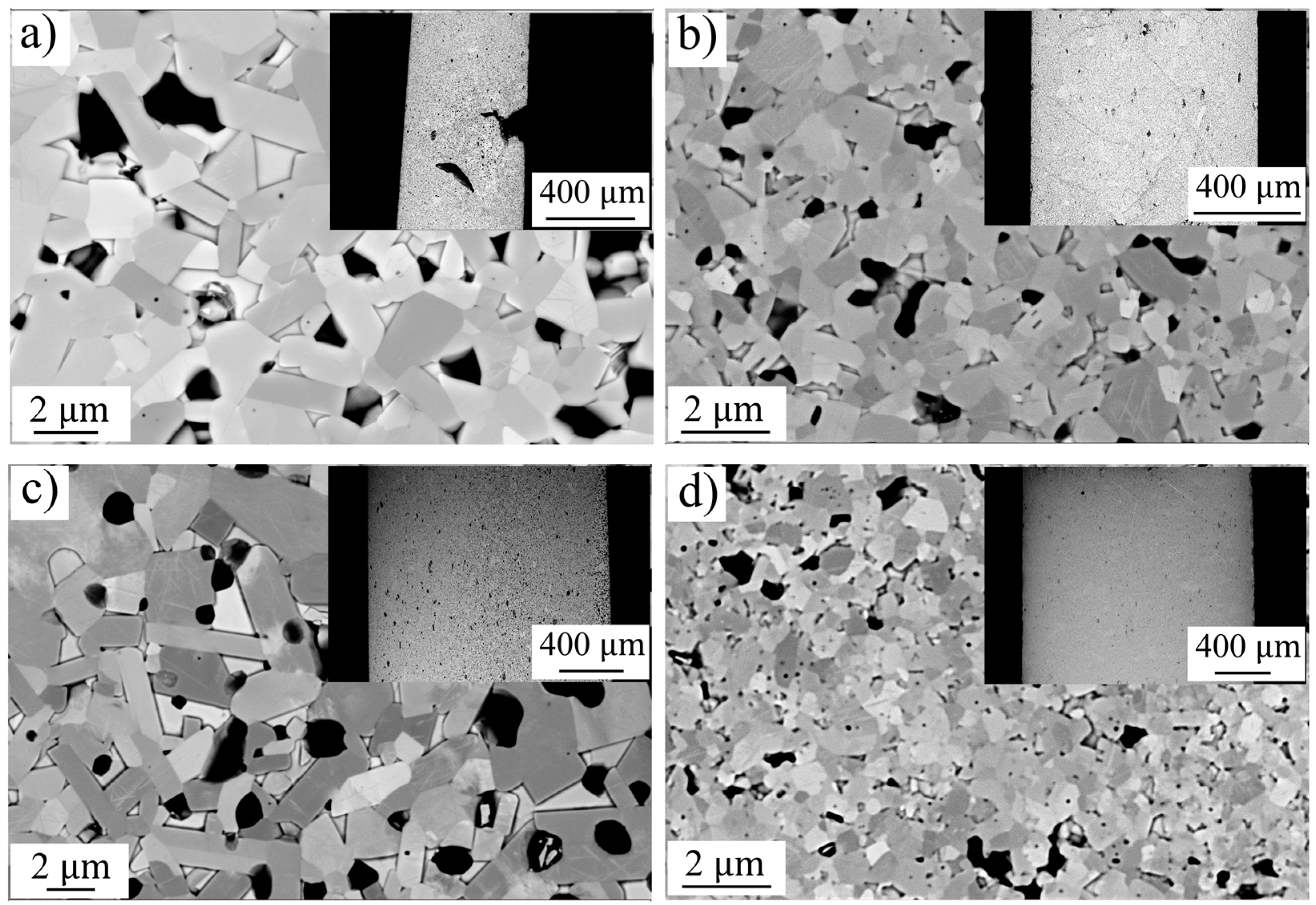
| UFS 1 | 2 s, 8.2 V | 6 s, 9.5 ± 0.8 V | 3 s, 5.6 V | 20 | 91.3% | Inhomogeneous microstructure (hot spots) |
| UFS 2 | 2 s, 1.9 V | 6 s, 10.9 ± 0.6 V | 3 s, 2.9 V | 20 | 94.6% | Homogenous |
| UFS 3 | 2 s, 1.2 V | 6.5 s, 11.6 ± 0.2 V | 3 s, 2.6 V | 20 | 98.1% | Fairly homogenous but partially decomposed |
| SPS 4 | heating rate of 100 °C/min, 5 min 2000 °C | 20 | 96.7% | Homogenous | ||
| Sample ID | UFS 1 * | UFS 2 | UFS 3 | SPS 4 |
|---|---|---|---|---|
| Average heating rate (°C/s) | 228.5 | 277.3 | 316.6 | 1.67 |
| Exp. Max Punch temperature (°C) | 1843 ± 36 | 2086 ± 42 | 2441 ± 48 | 2000 ± 40 |
| Sim. Maximum sample temperature (°C) | 2058 ± 40 * | 2383 ± 46 | 2753 ± 54 | N/A |
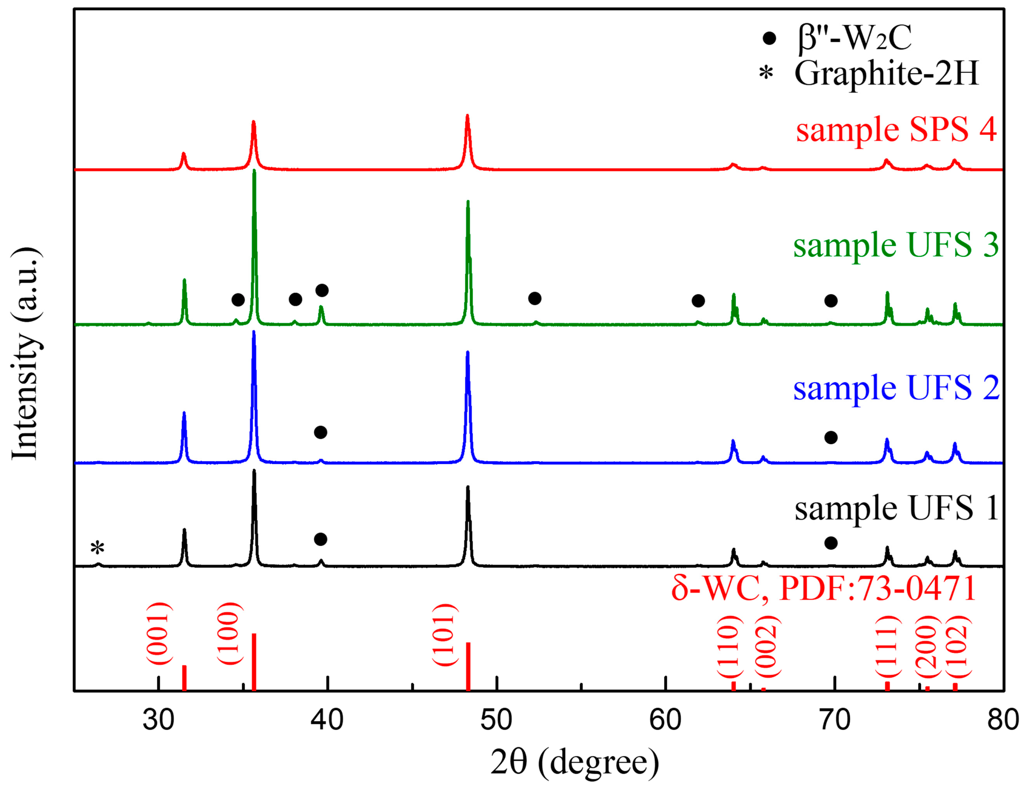
| (wt.%) | 82.6 | 95.6 | 89.5 | 100 |
| (wt.%) | 5.2 | 2.1 | 10.5 | 0 |
| Graphite-2H (wt.%) | 12.2 | 2.3 | 0 | 0 |
| Relative density (%) | 91.3 | 94.6 | 98.1 | 96.7 |
| Average grain size (μm) | 1.4 ± 0.1 | 0.81 ± 0.09 | 1.6 ± 0.11 | 0.6 ± 0.09 |
| Hardness (HV) | 1923 ± 59 | 2124 ± 134 | 1576 ± 65 | 2057 ± 47 |
| Energy consumed (MJ) | 0.41 ± 0.05 | 0.42 ± 0.05 | 0.47 ± 0.06 | 14.14 ± 0.5 |
Publisher’s Note: MDPI stays neutral with regard to jurisdictional claims in published maps and institutional affiliations. |
© 2021 by the authors. Licensee MDPI, Basel, Switzerland. This article is an open access article distributed under the terms and conditions of the Creative Commons Attribution (CC BY) license (https://creativecommons.org/licenses/by/4.0/).
Share and Cite
Deng, H.; Biesuz, M.; Vilémová, M.; Kermani, M.; Veverka, J.; Tyrpekl, V.; Hu, C.; Grasso, S. Ultrahigh Temperature Flash Sintering of Binder-Less Tungsten Carbide within 6 s. Materials 2021, 14, 7655. https://doi.org/10.3390/ma14247655
Deng H, Biesuz M, Vilémová M, Kermani M, Veverka J, Tyrpekl V, Hu C, Grasso S. Ultrahigh Temperature Flash Sintering of Binder-Less Tungsten Carbide within 6 s. Materials. 2021; 14(24):7655. https://doi.org/10.3390/ma14247655
Chicago/Turabian StyleDeng, Huaijiu, Mattia Biesuz, Monika Vilémová, Milad Kermani, Jakub Veverka, Václav Tyrpekl, Chunfeng Hu, and Salvatore Grasso. 2021. "Ultrahigh Temperature Flash Sintering of Binder-Less Tungsten Carbide within 6 s" Materials 14, no. 24: 7655. https://doi.org/10.3390/ma14247655
APA StyleDeng, H., Biesuz, M., Vilémová, M., Kermani, M., Veverka, J., Tyrpekl, V., Hu, C., & Grasso, S. (2021). Ultrahigh Temperature Flash Sintering of Binder-Less Tungsten Carbide within 6 s. Materials, 14(24), 7655. https://doi.org/10.3390/ma14247655