Abstract
The one-step hydrothermal method was used to synthesize Sn-doped TiO2 (Sn-TiO2) thin films, in which the variation in Sn content ranged from 0 to 7-wt % and, further, its influence on the performance of a dye-sensitized solar cell (DSSC) photoanode was studied. The deposited samples were analyzed by X-ray diffraction (XRD) and Raman spectroscopy, which confirmed the existence of the rutile phase of the synthesized samples with crystallite size ranges in between 20.1 to 22.3 nm. In addition, the bare and Sn-TiO2 thin films showed nanorod morphology. A reduction in the optical band gap from 2.78 to 2.62 eV was observed with increasing Sn content. The X-ray photoelectron spectroscopy (XPS) analysis confirmed Sn4+ was successfully replaced at the Ti4+ site. The 3-wt % Sn-TiO2 based DSSC showed the optimum efficiency of 4.01%, which was superior to 0.87% of bare and other doping concentrations of Sn-TiO2 based DSSCs. The present work reflects Sn-TiO2 as an advancing material with excellent capabilities, which can be used in photovoltaic energy conversion devices.
1. Introduction
Nanostructured, nanoporous semiconducting metal oxides with large surface areas and high diffusion rates are exclusively utilized as photoanode materials in dye-sensitized solar cells (DSSCs) [1]. Due to their cost-effectiveness, ease of manufacturing, and higher light conversion efficiency, DSSCs have become important alternatives to traditional silicon solar cells [2,3]. Various metal oxide semiconductors, such as ZnO, TiO2, Nb2O5, and SnO2, have been explored as photoanode materials for the development of high-performance DSSCs [4,5,6,7]. The contributing factors that establish the TiO2 semiconductor electrodes as the best photoanodes are their charge transport capability and chemical stability. TiO2 plays a very important role in DSSCs as it provides a high surface for adsorption of dye, acquiring electrons from the excited dye state, and quickly transferring to fluorine-doped tin oxide (FTO). Since TiO2 possesses a large bandgap of about 3.2 eV, it cannot be efficiently used in the visible light region but is more sensitive to the ultraviolet region. Hence, different research groups have synthesized TiO2 by various methods to improve the edge of absorption, mostly in the visible region. Doping of different elements in TiO2 is one of the best ways to reduce the bandgap and change the electronic structure, as well as to minimize the recombination rate and promote visible light absorption. All the above parameters could help to improve the charge transfer rate, high open-circuit voltage (Voc), and will be beneficial to enhance the DSSCs’ efficiency [8,9].
Suitable metal ions doping in the TiO2 can cover up the grain boundaries, which will generate oxygen vacancies and can improve the photoelectrochemical properties of the photoanodes. Many metals are used for doping in the TiO2 host lattice, but Sn is the most influential because of the close ionic radius of Ti4+ = 0.60 Å and Sn4+ = 0.69 Å, which helps to suitably replace Ti4+ in TiO2 with Sn4+ ions to generate a homogenous mixture [10]. The Sn doping enhances the charge transport, photon absorption, and improves the surface quantum-dots loading density of TiO2, which results in high photoelectrochemical efficiency [11,12]. Xiang et al. prepared Ta added TiO2, which shifts the potential negatively and raises the concentration of electrons of the TiO2 electrode, resulting in the reduction of the electron recombination rate and electron transport by Ta doping [13]. Su et al. reported improvement in the short circuit current density (Jsc) by Nb doping in TiO2. The enhancement in the Jsc is attributed to variation in the conduction band minimum (CBM), which facilitates electron transport and enhances the conductivity [14,15]. Different investigations have been done on doping TiO2 for the improvement of Voc and Jsc.
Different approaches have been used to synthesize Sn-doped TiO2 thin films which include spray pyrolysis [16,17], a microwave-assisted method [18], sol-gel [19,20,21], chemical co-precipitation [22], atomic layer deposition [23], a gas-phase oxidation method [24], and spin coating [25,26]. The Sn-doped TiO2 thin films have previously been used for different applications such as photocatalysis [27,28], gas sensing [29,30], lithium-ion batteries [31,32], and DSSCs [33,34]. Out of different synthesis processes available for the synthesis of TiO2 thin films, the hydrothermal method offers certain advantages such as the synthesis of rutile and anatase crystalline forms of TiO2 at relatively low temperatures, fine-tuning of morphology, and uniform coating onto the substrates [35].
In the present work, the hydrothermal method has been applied for the synthesis of Sn-doped TiO2 thin films using an acid catalyst. The Sn-TiO2 thin films are systematically synthesized by varying Sn concentration. The influence of Sn-doping concentration on structural, optical, morphological, and photoelectrical properties of Sn-TiO2 thin films has been examined. Improved photovoltaic performance is observed for the DSSCs fabricated with Sn-TiO2. Further, the Sn-doped TiO2 thin films have been successfully employed as photoelectrodes in DSSCs, which suggests a positive effect on its photovoltaic performance.
2. Methods
2.1. Synthesis of Sn-Doped TiO2 Films
Sn-doped TiO2 thin films were prepared by a single-step hydrothermal route by varying the Sn concentration in TiO2. FTO substrates were washed for 15 min by ultrasonic treatment using equal amounts of isopropyl alcohol, acetone, and deionized water (DIW) followed by drying in an N2 atmosphere. An equivalent volume of DIW and concentrated HCl was mixed and stirred for 10 min. In the aforementioned solution, 0.5 mL of titanium butoxide was mixed dropwise and constantly stirred for the next 30 min. The desired amount of tin (IV) chloride was poured into the aforesaid solution and stirred for the next 30 min until the solution becomes clear and homogeneous. The solution was then poured into the Teflon vessel and the ultrasonically cleaned FTO substrate was dipped in solution. The FTO substrate was kept inclined to the wall of the Teflon vessel with the conducting side facing upwards. The Teflon vessel was then fitted in the autoclave and heated for 3 h at 180 °C in a furnace. The autoclave was then allowed to cool naturally to room temperature. The FTO substrate coated with the desired material was then rinsed with DIW and dried at room temperature. The prepared films were finally annealed at 450 °C for 1 h. Sn-TiO2 thin films with different Sn concentrations (3, 5, and 7-wt %) were also prepared by the same procedure. Undoped TiO2 thin film was synthesized by the same procedure without the addition of the Sn precursor.
2.2. Cell Fabrication and Photovoltaic Measurements
Hydrothermally synthesized bare and Sn-doped TiO2 films with different concentrations of Sn were soaked in ethanolic 0.5 mM N719 dye (cisbis(isothiocyanato) bis (2,2′ bipyridyl-4,4′ dicarboxylato) ruthenium (II) bis-tetrabutylammonium, (Greatcell, Queanbeyan, Australia) solution for 24 h. After completion of the dye loading process, sensitized photoelectrodes were rinsed in acetonitrile and dried in air. DSSCs were fabricated by a two-electrode configuration comprising a working electrode and counter electrode. Dye-loaded bare TiO2 and Sn-TiO2 on FTO act as working electrodes, whereas platinum-coated FTO (Pt: FTO) acts as a counter electrode. Both these electrodes were sealed using polyacrylamide 1 mm spacers. The Pt: FTO electrodes were freshly prepared by drop-casting 0.5 mM hexachloroplatinic acid (H2PtCl6) dissolved in isopropanol solution onto FTO and heating at 400 °C for 20 min in air. The dye-loaded TiO2 photoanodes and platinum counter electrodes were closed with Surlyn thermoplastic (SX-1170-25, Solaronix, Aubonne, Switzerland) at specific temperatures and pressure. The electrolyte Iodolyte AN-50 was introduced through a pre-drilled Pt: FTO electrode opening. The system was eventually sealed with thermoplastics. The photovoltaic measurements were carried out at room temperature.
2.3. Characterizations
Rigaku Ultima X-ray diffractometer (Tokyo, Japan) with Cu Kα radiation, λ = 1.54 Å was used to investigate the structural characteristics. The WITec ALPHA 300 M Raman microscope was used to obtain the Raman spectra (excitation at 532 nm, 2.33 eV, Ulm, Germany). The chemical bonding of bare and doped TiO2 was examined using Fourier transform infrared spectroscopy (FTIR; Perkin Elmer 1760X spectrophotometer, Waltham, MA, USA) at wavelengths ranging from 400 cm−1 to 4000 cm−1. The surface morphologies were studied by using a field emission scanning electron microscope (FE-SEM, JSM-7001F, JEOL, Tokyo, Japan). The particle size was determined by using a JEM-2100F (JEOL, Tokyo, Japan) transmission electron microscope with an acceleration voltage of 125 kV. The Brunauer Emmett Teller (BET) N2 adsorption and desorption analyses were carried out by Quantachrome Instruments v10.0 (Florida, USA) to determine the surface area, pore size, and volume. The elemental composition of samples was analyzed using an X-ray photoelectron spectrometer (XPS, Thermo Scientific Inc., East Grinstead, UK) focused with Al (Kα) monochromator (1486.6 eV) and the spot size was variable (30–400 µm in 5 µm steps). The absorbance spectra were obtained by Jasco spectrophotometer (Jasco V-770, Tokyo, Japan) with a wavelength ranging from 200 to 800 nm. The photovoltaic measurements were carried out with a solar simulator (McScience K201 LAB50, Suwon, Korea) for 10 s with AM 1.5 G with 1 sun (100 mW cm−2) illumination intensity. An NREL-calibrated Si solar cell with a KG-5 filter was used as a reference cell.
3. Results and Discussion
The X-ray diffraction (XRD) patterns of bare and Sn-TiO2 thin films are shown in Figure 1a. The Sn-TiO2 thin films have a tetragonal rutile crystal structure, which is the same as bare TiO2 (JCPDS No. 21-1276). Sn doping slightly affects the rutile TiO2 crystal structure. The (002) reflection of the Sn-TiO2 film is slightly displaced to a higher 2θ value and its intensity has decreased, as the concentration of Sn doping has increased from 1 to 7-wt %. The Sn doping has increased the intensity of (110) reflection. Due to Sn doping, only a slight variation in the lattice constants of bare-TiO2 thin films is observed, signifying the partial replacement of Ti4+ sites by Sn4+ cations due to their close ionic radii. The relevant crystal structure parameters, like the crystallite size, lattice constant, and cell volume, are shown in Table S1. The average crystallite size for the bare, 1, 3, 5, and 7-wt % Sn-TiO2 is determined as 20.1, 20.7, 21.2, 21.7, and 22.3 nm, respectively. This implies that with increasing Sn content, the average crystallite size of the samples increases. In all the samples, the rutile phase is the dominating phase, as shown in Figure 1a.
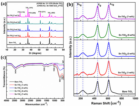
Figure 1.
(a) XRD patterns, (b) Raman spectra, and (c) FT-IR spectra of hydrothermally synthesized bare TiO2, 1-wt %, 3-wt %, 5-wt %, and 7-wt % Sn-TiO2 thin films.
Figure 1b displays the Raman spectra of bare and Sn-TiO2 thin films. The prominent reflections positioned at 144, 448, and 610 cm−1 corresponding to the B1g, Eg, and A1g vibrational modes of the rutile phase, respectively. The intense reflections at 448 and 610 cm−1 represent the O–Ti–O bending and Ti–O stretching vibrations of the rutile phase, respectively [36]. The stretching vibration at 233 cm−1 can be assigned to compound vibration generated by a multi-phonon process, signifying the rutile phase of TiO2 [37]. The absence of characteristic reflections for SnO2 at 470 cm−1, 574 cm−1, 636 cm−1, and 776 cm−1 [38] confirms the non-existence of crystalline SnO2 due to minimal Sn doping concentration.
Figure 1c represents the FT-IR spectra of bare and Sn-TiO2 thin films in the 400–4000 cm−1 range. The bands located at 1600 and 3400 cm−1 can be assigned to the stretching and bending vibration of water molecules, respectively. In bare and Sn-TiO2, the bands at 1632 cm−1 represent the bending vibration of a water molecule and stretching vibration of O–H. The presence of a band over the range of 1022 to 1100 cm−1 indicates the evidence of Ti–O–Ti vibrations in the films [39]. Peaks observed in the 400–800 cm−1 range can be ascribed to vibration modes of Ti–O, Ti–O–Ti, Sn–O, and Ti–O–Sn bonds. The Sn doping into TiO2 results in a peak shift to a lower wavenumber observed in the FT-IR spectra of Sn-TiO2 [40]. The shifting of the peak from 662 to 651 cm−1 for Sn–TiO2 films confirms the Ti–O–Sn bond formation [18]. The band at 1460 cm−1 corresponds to the stretching vibration of the Ti–O–Ti, which has shifted to 1457 cm−1 because of Sn4+ doping [41]. The band observed at the low frequency region of FTIR spectra at 530 and 427 cm−1 corresponds to bending vibrations of Ti–O and Ti–O–Ti bonds [42].
Figure 2a presents the UV-Visible spectra of bare and Sn-TiO2 thin films prepared with different Sn doping concentrations. A small redshift is observed for the thin films and absorption band edges have broadened to a visible region with the rise in Sn concentration. This effect is mainly caused by Sn4+ doping, which generates a temporally indirect energy gap in the mid-gap zone of TiO2, facilitating an electron excitation and lowering the energy barrier needed for electrons to be excited from the valence band (VB) to the conduction band (CB). In comparison with bare TiO2, the absorption edge of Sn-doped TiO2 thin films has slightly shifted to a longer wavelength. The desired doping concentration thus increases the efficiency of cells in the visible region [43]. Figure S1 shows the Tauc plots of bare and Sn-TiO2 thin films, from which it is inferred that the bandgap has reduced from 2.78 to 2.62 eV with the increase in Sn content. The reduction in the bandgaps indicates that the minimum energy is required for the excitation of electrons. It facilitates the electron transfer from VB to CB.
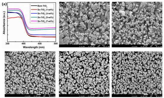
Figure 2.
(a) UV-visible absorption spectra of bare TiO2, 1-wt %, 3-wt %, 5-wt %, and 7-wt % Sn-TiO2 thin films. FE-SEM images of (b) bare TiO2 (c) 1-wt %, (d) 3-wt %, (e) 5-wt %, and (f) 7-wt % Sn-TiO2 thin films.
In addition, the effect of Sn content on the surface morphology of the TiO2 thin films was determined using the FE-SEM technique as presented in Figure 2b–f. The FE-SEM images at a magnification of ×50,000 are shown in Figure S2a–e. The surface morphology appeared in the form of 1D nanorods for the bare TiO2, whereas for the Sn-TiO2 thin films, 3D flower-like nanorods are noticed, as shown in Figures S2a and S3a,b, respectively. The detailed growth mechanism of TiO2 nanorods has previously been explored [44]. The consistent growth of Sn-TiO2 nanorods is observed. These nanorods are mixed and assisted together to offer more interspace. Each nanorod is composed of a set of thinner nanorods with square top facets. These nanorods are nearly uniform, well-aligned, and uniformly distributed on the surface of the films. Nanorod morphology provides a larger surface area which enhances the efficiency of DSSCs by efficient transport of electrons. The whole surface of FTO is covered with well-aligned nanorods. The FTO substrate provides numerous nucleation centers which initiate the growth of the TiO2 nanorods. As shown in Figure 2b–f and Figure S2, the nanorods appeared less normal to the substrate, which can be attributed to the decreased intensity of (002) reflections of Sn-TiO2.
Figure 3a,b shows the cross-section of 3-wt % Sn-TiO2 and 7-wt % Sn-TiO2 thin films, respectively, which indicates the formation of well-aligned nanorods. The cross-sectional view of 3-wt % and 7-wt % Sn-TiO2 thin films shows that the nanorods have grown almost perpendicular to the substrate. The average length and diameter of the nanorods are determined as 2.3 µm and 180 nm, respectively, for 3-wt % Sn-TiO2. For 7-wt % Sn-TiO2 thin films, the average length and diameter of the nanorods are estimated as 2.1 µm and 150 nm, respectively. The HR-TEM image of 7-wt % Sn-TiO2 thin films is depicted in Figure 3c. It reveals that numerous nanorods come together and form a bundle of nanorods. These nanorods are moderately uniform, with an average length of nearly 2 µm, and an average diameter of nearly 150 to 250 nm. Figure 3d displays the HR-TEM image of 7-wt % Sn-TiO2 thin films, in which lattice fringes of (110) reflection with interplanar spacing 0.33 nm are seen, which is a characteristic of rutile TiO2.
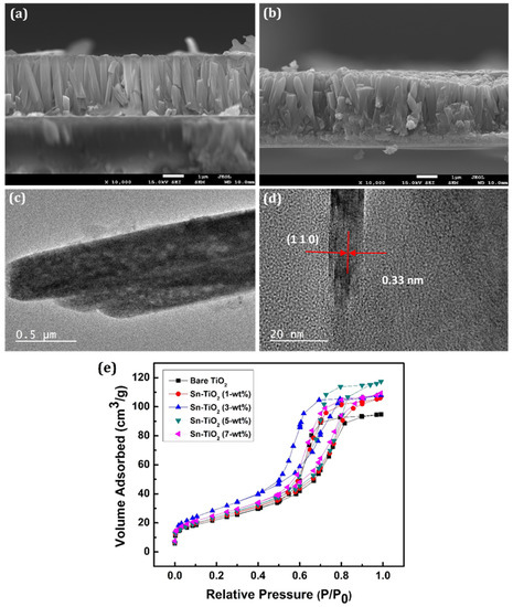
Figure 3.
SEM cross-section of (a) 3-wt % (b) 7-wt % Sn-TiO2 thin films. HR-TEM image of 7-wt % Sn-TiO2 (c) Bundles of nanorods and (d) Lattice fringes with interplanar spacing of (110) reflection. (e) The N2 adsorption-desorption isotherms of the bare TiO2 and Sn-TiO2 thin films with varying Sn concentration.
The BET analyses of TiO2 and Sn-TiO2 samples are carried out to investigate the changes in the surface area and pore diameter raised due to Sn doping. Figure 3e exhibits the BET N2 adsorption-desorption isotherms as representations of relative pressure (P/P0) against a volume of gas adsorbed at equilibrium. The presence of mesopores in the bare and Sn-TiO2 samples is confirmed by the presence of type IV isotherms with a significant hysteresis loop. The average specific surface areas of the polycrystalline bare-TiO2, 1, 3, 5, and 7-wt % Sn-TiO2 samples are determined as 80.69, 84.11, 107.57, 88.88, and 92.30 m2 g−1, respectively. The average pore volumes and mean pore diameters of bare-TiO2, 1, 3, 5, and 7-wt % Sn-TiO2 samples are calculated as 0.146, 0.165, 0.166, 0.181, and 0.169 cm3 g−1, and 7.25, 7.86, 6.20, 8.16, and 7.33 nm, respectively. It is observed that the surface area (SBET), pore-volume, and pore diameter of the bare and Sn-TiO2 thin films vary with Sn content. The 3-wt % Sn-TiO2 has the highest SBET value, suitable for effective dye adsorption. The values of specific surface area, pore-volume, and mean pore diameter of bare-TiO2 and Sn-TiO2 samples have been illustrated in Table 1.

Table 1.
Surface area, pore volume, and pore diameters of bare-TiO2 and Sn-TiO2 thin films.
The XPS technique is used to assess the chemical states and elemental composition of the prepared films. Figure S4 shows the survey spectrum of 7-wt % Sn-TiO2 thin film, which confirms the existence of titanium, tin, and oxygen elements in the synthesized film. The Sn 3d3/2 and Sn 3d5/2 peaks are detected for Sn-TiO2 thin films and are shown in the inset of Figure S4. Figure 4a displays the deconvoluted XPS spectra of Ti 2p of bare TiO2 and 7-wt % Sn-TiO2 thin films.
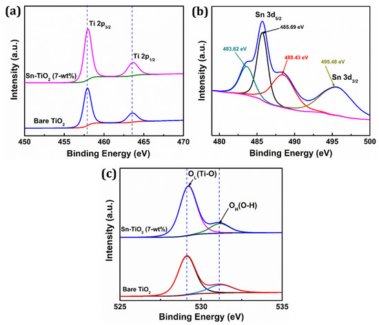
Figure 4.
High-resolution XPS spectra of (a) Ti 2p, (b) Sn 3d, (c) O 1s fitting of bare TiO2 and 7-wt % Sn-TiO2 thin films.
The binding energy for Ti 2p3/2 and Ti 2p1/2 for bare TiO2 is found to be 457.87 and 463.53 eV, respectively, whereas for Sn-TiO2, it is found to be 458.02 and 463.72 eV, respectively. When compared to the spectra of bare-TiO2, the two peaks of the Ti 2p spectra of 7-wt % Sn-TiO2 show a slight positive shift, which is most likely due to the interaction between Ti, O, and Sn atoms. It reveals that Sn doping induces a peak shift of Ti 2p to higher binding energy and indicates the +4 oxidation state of titanium [45]. This positive shift implies that electron loss from Ti4+ in the oxide is due to the existence of Sn4+ with considering their electronegativity difference (Ti = 1.54 and Sn = 1.96) [46]. The deconvoluted narrow scan XPS spectrum of Sn 3d is shown in Figure 4b. The binding energy 485.69 and 495.48 eV corresponds to Sn 3d5/2 and Sn 3d3/2 and confirms that Sn4+ is incorporated into the TiO2 lattice. Also, the deconvoluted Sn3d5/2 reflects two additional peaks at 483.62 and 488.43 eV, which are attributed to presence of Sn2+ and Sn4+ oxidation states, respectively [47,48]. Figure 4c represents the deconvoluted O 1s spectra of bare TiO2 and 7-wt % Sn-TiO2 thin films. The intense peaks observed at 529.10 eV and 529.23 eV are due to lattice oxygen (Ti–O) and the less intense peaks at 531.14 eV and 531.18 eV correspond to adsorbed hydroxyl (–OH) group in the bare-TiO2 and Sn-TiO2 thin films, respectively. The peak shifting to higher binding energy due to Sn doping is observed for Sn-TiO2 thin films. These findings support the existence of the Ti–O–Sn bond in Sn-doped films because of the replacement of Ti4+ by Sn4+.
The graphical view of 1D and 3D Sn-TiO2 nanorods for the application of DSSCs is depicted in Figure 5a. The 3D Sn-TiO2 flower-like morphology comprises single-crystalline nanorods, which enhance electron mobility and photon harvesting through light scattering (Figure S5). Furthermore, the flower-like morphology provides a higher surface area for dye loading, and thus more absorption takes place towards the visible region.
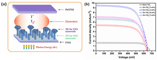
Figure 5.
(a) The graphical view of 1D and 3D Sn-TiO2 nanorods based DSSCs (b) The Photocurrent density–photovoltage (J–V) curves of dye-sensitized bare TiO2 and Sn-TiO2 photoelectrodes with different Sn concentrations.
Figure 5b represents the J–V curves of the DSSCs constructed using bare-TiO2 and 1, 3, 5, and 7-wt % Sn-TiO2 thin films sensitized with ruthenium dye N719. Table 2 summarizes the different DSSCs performance parameters of bare-TiO2 and 1, 3, 5, and 7-wt % Sn-TiO2 thin films. The cell configurations employed to measure J–V characteristics were FTO/TiO2/N719 Dye/I--I3-/Pt: FTO and FTO/Sn-TiO2/N719 dye/I--I3-/Pt: FTO.
Table 2.
Performance characteristics of DSSCs based on the bare-TiO2 and Sn-TiO2 photoelectrodes with varying Sn concentrations.
The magnitude of the Jsc observed is 1.65 mA cm−2 for the bare-TiO2 and 5.35, 9.49, 6.66, and 7.08 mA cm−2 for 1, 3, 5, and 7-wt % Sn-TiO2 thin films, respectively. The DSSCs with bare TiO2 thin films provided power conversion efficiency (PCE) of 0.87% with a fill factor (FF) of 77.70%. It is observed that the variation in the Jsc values is governed by variation in the Sn concentration. As compared to bare TiO2, the enhancement in the PCE of Sn-TiO2 based DSSCs is observed. The possible reason for the enhancement in the PCE of Sn-TiO2 is ascribed to the large surface area of vertically grown nanorods that may enhance the output photocurrent. Moreover, the morphology observed for 3-wt % Sn-TiO2 thin films is a uniformly distributed, well-aligned bundle of nanorods (Figure S3a), which offers a greater surface area for dye loading and facilitates the transport of electrons. For the DSSCs fabricated with 3-wt % Sn-TiO2 thin films, the highest Jsc of 9.49 mA cm−2 is observed with Voc of 0.64 V, and it has provided the highest PCE of 4.01%.
The Sn-TiO2 nanorods are found to be capable of enhancing the efficiency of DSSCs by providing a confined path for the transport of charge carriers with redox electrolyte and rapid charge separation. The PCE of Sn-TiO2 photoelectrode is marginally higher than bare TiO2 photoelectrodes due to a modest rise in defect states, leading to less recombination in the trapped sites. The interaction of Sn with the TiO2 lattice generates a shift in the Fermi level of TiO2. Consequently, the Sn captures the electron within the conduction band of TiO2. In the meantime, the equilibrium of the Fermi level is achieved [49]. Electron capture by Sn extends the lifespan of holes and reduces hole–electron recombination. Hence, noticeable improvement in the Jsc and Voc is observed. Doped photoelectrode cells have a much higher performance than pure photoelectrode cells due to enhanced chemisorptions onto doped TiO2 [50]. The substitution of Sn causes distortion in the TiO2 lattice, creates oxygen vacancies, and contributes to enhanced photo activity. The improvement of the Sn-doped photoelectrode-based cell implies that doping may generate a donor level, leading to a greater concentration of the carrier with a decrease in film resistance [51]. For ideal DSSCs, the Rs (series resistance) should be low, and Rsh (shunt resistance) should be a maximum. The current-voltage characteristics depends upon Rs and Rsh resistance. A lower Rs enhances current flow in the circuit, and high Rsh provides fewer shorts or leaks in the device. In an ideal cell, the Rs value is close to zero, and Rsh approaches infinity. The Rs and Rsh are measured by the J–V curve and can be determined by Equations (1) and (2).
The bare-TiO2 showed the lowest efficiency with a high Rs value of 168.66 Ω, whereas the 3-wt % Sn-TiO2 films exhibited higher efficiency with a low Rs value of 56.2 Ω. These findings confirmed that low Rs and high Rsh determine the PCE of the DSSCs.
The tin doping reduces the band gap of TiO2. The charge transfer from the bulk to the surface of nanorods reduces the bandgap and facilitates the photogeneration process. The concentration of impurities increases with dopant concentration. Such impurities act as charge trapping sites for hole–electron recombination. If a doping content is more or less than 3-wt %, the recombination rate is more severe and results in a reduction in Voc and Jsc and thus affects the PCE. Therefore, 3-wt % Sn-TiO2 thin films showed the optimum quantity of dopant, which gives better PCE.
4. Conclusions
We have designed Sn-TiO2 nanorod morphology-based DSSCs using a simple, low temperature, and low-cost hydrothermal method. The synthesized bare and Sn-TiO2 thin films with nanorod morphology have been successfully sensitized with N719 dye using the piranha solution etching process. The Sn-doped TiO2 facilitates the rutile phase formation at a certain annealing temperature and reduces the band gap of TiO2. The 3-wt % Sn-TiO2 showed a specifically large surface area of about 107.57 m2 g−1 which adsorbs more dye and thereby improves the performance of DSSCs. Photovoltaic studies showed considerable enhancement in PCE for the 3-wt % sample with a maximum Jsc of 9.49 mA cm−2 with a Voc of 0.64 V and a PCE of 4.01%. Hence, Sn-TiO2 photoelectrodes will be promising photoelectrode materials for the development of highly efficient DSSCs.
Supplementary Materials
The following are available online at https://www.mdpi.com/article/10.3390/ma14216282/s1, Figure S1: Tauc plots showing bandgap of synthesized thin films having a different concentration of Sn; Figure S2: FE-SEM images of (a) bare TiO2, (b) 1-wt %, (c) 3-wt %, (d) 5-wt % and (e) 7-wt % Sn-TiO2 thin films with magnification of ×50,000; Figure S3: FE-SEM images of (a) 3-wt % Sn-TiO2 and (b) 7-wt % Sn-TiO2 showing epitaxial growth of nanorods forming flower-like morphology; Figure S4: XPS survey spectrum of 7-wt % Sn-TiO2; Figure S5: Morphological variation from nanorods to nano-flower; Table S1: Crystal structure parameters of bare-TiO2 and Sn-TiO2 thin films.
Author Contributions
Conceptualization, S.B.W., B.M.S. and R.K.M.; methodology, S.B.W., R.P.P., S.S.M., B.M.S. and R.K.M.; formal analysis, S.B.W., V.G.P., S.S.M., P.S.M., C.-K.H. and H.-H.P.; investigation, S.B.W., V.G.P., S.S.M., C.-K.H., B.M.S. and R.K.M.; data curation, S.B.W., B.M.S., R.P.P., H.-H.P. and R.K.M.; writing—original draft preparation, S.B.W., H.-H.P., B.M.S. and R.K.M., writing—review and editing, S.B.W., H.-H.P., B.M.S., A.V.M., V.G.P., C.-K.H., P.S.M., S.S.M. and R.K.M.; supervision, B.M.S., H.-H.P., A.V.M. and R.K.M. All authors have read and agreed to the published version of the manuscript.
Funding
This research received no external funding.
Institutional Review Board Statement
Not applicable.
Informed Consent Statement
Not Applicable.
Data Availability Statement
Inside the article, data is included.
Acknowledgments
This work was supported by the National Research Foundation of Korea Grant funded by the Government of South Korea (NRF 2020R1A5A1019131). This research is also supported by the National Research Foundation of Korea (NRF) Korean government (2020R1A2C2004880). This work was also supported by Priority Research Centers Program through the National Research Foundation of Korea (NRF) funded by the Ministry of Education, Science and Technology (NRF-2018R1A6A1A03024334). The author SBW thankful to D. P. Nade, Rohit R. Powar, Sambhaji M. Pawar for fruitful discussion.
Conflicts of Interest
The authors declare no conflict of interest.
References
- Oelhafen, P.; Schüler, A. Nanostructured materials for solar energy conversion. Sol. Energy 2005, 79, 110–121. [Google Scholar] [CrossRef]
- O’ Regan, B.C.; Durrant, J.R. Kinetic and energetic paradigms for dye-sensitized solar cells: Moving from the ideal to the real. Acc. Chem. Res. 2009, 42, 1799–1808. [Google Scholar] [CrossRef]
- Zhang, S.; Yang, X.; Numata, Y.; Han, L. Highly efficient dye-sensitized solar cells: Progress and future challenges. Energy Environ. Sci. 2013, 6, 1443–1464. [Google Scholar] [CrossRef]
- Marimuthu, T.; Anandhan, N.; Thangamuthu, R.; Surya, S. Influence of solution viscosity on hydrothermally grown ZnO thin films for DSSC applications. Superlattices Microstruct. 2016, 98, 332–341. [Google Scholar] [CrossRef]
- Mali, S.S.; Betty, C.A.; Bhosale, P.N.; Patil, P.S. Eosin-Y and N3-Dye sensitized solar cells (DSSCs) based on novel nanocoral TiO2: A comparative study. Electrochim. Acta 2012, 59, 113–120. [Google Scholar] [CrossRef]
- Panetta, R.; Latini, A.; Pettiti, I.; Cavallo, C. Synthesis and characterization of Nb2O5mesostructures with tunable morphology and their application in dye-sensitized solar cells. Mater. Chem. Phys. 2017, 202, 289–301. [Google Scholar] [CrossRef]
- Qi, T.; Wang, Q.; Zhang, Y.; Wang, D.; Yang, R.; Zheng, W. Growth of flower-like SnO2 crystal and performance as photoanode in dye-sensitized solar cells. Mater. Des. 2016, 112, 436–441. [Google Scholar] [CrossRef]
- Akila, Y.; Muthukumarasamy, N.; Agilan, S.; Senthilarasu, S.; Velauthapillai, D. Zirconium oxide post treated tin doped TiO2 for dye sensitized solar cells. Mater. Sci. Semicon. Proc. 2017, 57, 24–31. [Google Scholar] [CrossRef]
- Changneng, Z.; Chen, S.; Mo, L.; Huang, Y.; Tian, H.; Hu, L.; Huo, Z.; Dai, S.; Kong, F.; Pan, X. Charge recombination and band-edge shift in the dye-sensitized Mg2+ doped TiO2 solar cells. J. Phys. Chem. C 2011, 115, 16418–16424. [Google Scholar]
- Mehraz, S.; Konsong, P.; Taleb, A.; Dokhane, N.; Sikong, L. Large scale and facile synthesis of Sn doped TiO2 aggregates using hydrothermal synthesis. Sol. Energy Mater. Sol. Cells 2019, 189, 254–262. [Google Scholar] [CrossRef]
- Liu, X.; Kong, W.; Zhao, G.; Xuan, J.; Zhao, Y.; Zhou, T.; Xiu, J.; Wang, J.; Sun, M.; Yin, G. Enhanced CdS quantum dots loading density and charge transport by Sn4+ doping improve the photoelectrochemical performance of TiO2 nanosheets with highly exposed {001} facets. Appl. Surf. Sci. 2019, 486, 28–36. [Google Scholar] [CrossRef]
- Duan, Y.; Fu, N.; Zhang, Q.; Fang, Y.; Zhou, X.; Lin, Y. Influence of Sn source on the performance of dye-sensitized solar cells based on Sn-doped TiO2 photoanodes: A strategy for choosing an appropriate doping source. Electrochim. Acta 2013, 107, 473–480. [Google Scholar] [CrossRef]
- Xiang, P.; Ma, W.; Xiao, T.; Jiang, L.; Tan, X.; Shu, T. Ta-doped hierarchical TiO2 spheres for dye-sensitized solar cells. J. Alloys. Compd. 2016, 656, 45–50. [Google Scholar] [CrossRef]
- Su, H.; Huang, Y.T.; Chang, Y.H.; Zhai, P.; Hau, N.Y.; Cheung, P.C.H.; Yeh, W.T.; Wei, T.C.; Feng, S.P. The Synthesis of Nb-doped TiO2 Nanoparticles for Improved-Performance Dye Sensitized Solar Cells. Electrochim. Acta 2015, 182, 230–237. [Google Scholar] [CrossRef]
- Wategaonkar, S.B.; Parale, V.G.; Pawar, R.P.; Mali, S.S.; Hong, C.K.; Powar, R.R.; Moholkar, A.V.; Park, H.H.; Sargar, B.M.; Mane, R.K. Structural, morphological, and optical studies of hydrothermally synthesized Nb-added TiO2 for DSSC application. Ceram. Int. 2021, 47, 22580–22592. [Google Scholar] [CrossRef]
- Arunachalam, A.; Dhanapandian, S.; Manoharan, C. Effect of Sn doping on the structural, optical and electrical properties of TiO2 films prepared by spray pyrolysis. Physica E 2016, 76, 35–36. [Google Scholar] [CrossRef]
- Dhanapandian, S.; Arunachalam, A.; Manoharan, C. Highly oriented and physical properties of sprayed anatase Sn-doped TiO2 thin films with an enhanced antibacterial activity. Appl. Nanosci. 2016, 6, 387–397. [Google Scholar] [CrossRef]
- Kadam, A.; Dhabbe, R.; Shin, D.; Garadkar, K.; Park, J. Sunlight driven high photocatalytic activity of Sn doped N-TiO2 nanoparticles synthesized by a microwave assisted method. Ceram. Int. 2017, 43, 5164–5172. [Google Scholar] [CrossRef]
- Mahanty, S.; Roy, S.; Sen, S. Effect of Sn doping on the structural and optical properties of sol–gel TiO2 thin films. J. Cryst. Growth 2014, 261, 77–81. [Google Scholar] [CrossRef]
- Tripathi, A.K.; Mathpal, M.C.; Kumar, P.; Singh, M.K.; Soler, M.A.G.; Agarwal, A. Structural, optical and photoconductivity of Sn and Mn doped TiO2 nanoparticles. J. Alloys. Compd. 2015, 622, 37–47. [Google Scholar] [CrossRef]
- Liao, Y.H.; Chang, Y.H.; Lin, T.H.; Chan, S.H.; Lee, K.M.; Hsu, K.H.; Hsu, J.F.; Wu, M.C. Boosting the power conversion efficiency of perovskite solar cells based on Sn doped TiO2 electron extraction layer via modification the TiO2 phase junction. Solar Energy 2020, 205, 390–398. [Google Scholar] [CrossRef]
- Yang, Y.; Li, H.; Zhao, H.; Qu, R.; Zhang, S.; Hu, W.; Yu, X.; Zhu, X.; Liu, S.; Zheng, C.; et al. Structure and crystal phase transition effect of Sn doping on anatase TiO2 for dichloromethane decomposition. J. Hazard. Mater. 2019, 371, 156–164. [Google Scholar] [CrossRef]
- Lee, D.K.; Kwon, S.H.; Ahn, J.H. Growth of rutile-TiO2 thin films via Sn doping and insertion of ultra-thin SnO2 interlayer by atomic layer deposition. Mater. Lett. 2019, 246, 1–4. [Google Scholar] [CrossRef]
- Jiang, H.B.; Xing, J.; Chen, Z.P.; Tian, F.; Cuan, Q.; Gong, X.Q.; Yang, H.G. Enhancing photocatalytic activity of Sn doped TiO2dominated with {1 0 5} facets. Catal. Today 2014, 225, 18–23. [Google Scholar] [CrossRef]
- Sayilkan, F.; Asilturk, M.; Tatar, P.; Kiraz, N.; Arpac, E.; Sayilkan, H. Photocatalytic performance of Sn-doped TiO2 nanostructured mono and double layer thin films for Malachite Green dye degradation under UV and vis-lights. J. Hazard. Mater. 2007, 144, 140–146. [Google Scholar] [CrossRef]
- Ranjitha, A.; Thambidurai, M.; Shini, F.; Muthukumarasamy, N.; Velauthapillai, D. Effect of doped TiO2 film as electron transport layer for inverted organic solar cell. Mater. Sci. Energy Technol. 2019, 2, 385–388. [Google Scholar] [CrossRef]
- Sengele, A.; Rober, D.; Keller, N.; Colbeau-Justi, C.; Kellera, V. Sn-doped and porogen-modified TiO2 photocatalyst for solar light elimination of sulfurediethyle as a model for chemical warfare agent. Appl. Catal. B Environ. 2019, 245, 279–289. [Google Scholar] [CrossRef]
- Rimoldi, L.; Pargoletti, E.; Meroni, D.; Falletta, E.; Cerrato, G.; Turco, F.; Cappelletti, G. Concurrent role of metal (Sn, Zn) and N species in enhancing the photocatalytic activity of TiO2 under solar light. Catal. Today 2018, 313, 40–46. [Google Scholar] [CrossRef]
- Benkara, S.; Zerkout, S.; Ghamri, H. Synthesis of Sn doped ZnO/TiO2 nanocomposite film and their application to H2 gas sensing properties. Mater. Sci. Semicon. Proc. 2013, 16, 1271–1279. [Google Scholar] [CrossRef]
- Zakrzewska, K.; Radecka, M.; Rekas, M. Effect of Nb, Cr, Sn additions on gas sensing properties of TiO2 thin films. Thin Solid Films 1997, 310, 161–166. [Google Scholar] [CrossRef]
- Lubke, M.; Johnson, I.; Makwana, N.M.; Brett, D.; Shearing, P.; Liu, Z.; Darr, J.A. High power TiO2 and high capacity Sn-doped TiO2 nanomaterial anodes for lithium-ion batteries. J. Power Sources 2015, 294, 94–102. [Google Scholar] [CrossRef]
- Kyeremateng, N.A.; Vacandio, F.; Sougrati, M.T.; Martinez, H.; Jumas, J.C.; Knauth, P.; Djenizian, T. Effect of Sn-doping on the electrochemical behaviour of TiO2 nanotubes as potential negative electrode materials for 3D Li-ion micro batteries. J. Power Sources 2013, 224, 269–277. [Google Scholar] [CrossRef]
- Ako, R.T.; Ekanayake, P.; Young, D.J.; Hobley, J.; Chellappan, V.; Tan, A.L.; Gorelik, S.; Subramanian, G.S.; Lim, C.M. Evaluation of surface energy state distribution and bulk defect concentration in DSSC photoanodes based on Sn, Fe, and Cu doped TiO2. Appl. Surf. Sci. 2015, 351, 950–961. [Google Scholar] [CrossRef]
- Ni, S.; Guo, F.; Wang, D.; Jiao, S.; Wang, J.; Zhang, Y.; Wang, B.; Feng, P.; Zhao, L. Modification of TiO2 Nanowire Arrays with Sn Doping as Photoanode for Highly Efficient Dye-Sensitized Solar Cells. Crystals 2019, 9, 113. [Google Scholar] [CrossRef]
- Li, J.; Xu, X.; Liu, X.; Yu, C.; Yan, D.; Sun, Z.; Pan, L. Sn doped TiO2 nanotube with oxygen vacancy for highly efficient visible light photocatalysis. J. Alloy. Compd. 2016, 679, 454–462. [Google Scholar] [CrossRef]
- Mayabadi, A.H.; Waman, V.S.; Kamble, M.M.; Ghosh, S.S.; Gabhale, B.B.; Rondiya, S.R.; Rokade, A.V.; Khadtare, S.S.; Sathe, V.G.; Pathan, H.M.; et al. Evolution of structural and optical properties of rutile TiO2 thin films synthesized at room temperature by chemical bath deposition method. J. Phys. Chem. Solids 2014, 75, 182–187. [Google Scholar] [CrossRef]
- Mali, S.S.; Betty, C.A.; Bhosale, P.N.; Patil, P.S. Hydrothermal synthesis of rutile TiO2 with hierarchical microspheres and their characterization. CrystEnggComm 2011, 13, 6349–6351. [Google Scholar] [CrossRef]
- Huang, B.X.; Tornatore, P.; Li, Y.S. IR and Raman spectroelectrochemical studies of corrosion films on tin. Electrochim. Acta 2000, 46, 671–679. [Google Scholar] [CrossRef]
- Tripathi, A.K.; Mathpal, M.C.; Kumar, P.; Agrahari, V.; Singh, M.K.; Mishra, S.K.; Ahmad, M.M.; Agarwal, A. Photoluminescence and photoconductivity of Ni doped titaniananoparticles. Adv. Mater. Lett. 2015, 6, 201–208. [Google Scholar] [CrossRef]
- Lin, W.; Zhang, Y.F.; Li, Y.; Ding, K.N.; Li, J.Q. Structural characterizations and electronic properties of Ti-doped SnO2 (110) surface: A first-principles study. J. Chem. Phys. 2006, 124, 054704. [Google Scholar] [CrossRef]
- Maragatha, J.; Rajendran, S.; Endo, T.; Karuppuchamy, S. Microwave synthesis of metal doped TiO2 for photocatalytic applications. J. Mater. Sci Mater. Electron. 2017, 28, 5281–5287. [Google Scholar] [CrossRef]
- Maira, A.J.; Coronado, J.M.; Augugliaro, V.; Yeung, K.L.; Conesa, J.C.; Soria, J. Fourier transform infrared study of the performance of nanostructured TiO2 particles for the photocatalytic oxidation of gaseous toluene. J. Catal. 2001, 202, 413–420. [Google Scholar] [CrossRef]
- Gu, D.; Zhu, Y.; Xu, Z.; Wang, N.; Zhang, C. Effects of ion doping on the optical properties of dye-sensitized solar cells. Adv. Mater. Phys. Chem. 2014, 4, 187. [Google Scholar] [CrossRef]
- Wategaonkar, S.B.; Pawar, R.P.; Parale, V.G.; Nade, D.P.; Sargar, B.M.; Mane, R.K. Synthesis of rutile TiO2 nanostructures by single step hydrothermal route and its characterization. Mater. Today-Proc. 2020, 23, 444–451. [Google Scholar] [CrossRef]
- Sanjines, R.; Tang, H.; Berger, H.; Gozzo, F.; Margaritondo, G.; Levy, F. Electronic structure of anatase TiO2 oxide. J. Appl. Phys. 1994, 75, 2945–2951. [Google Scholar] [CrossRef]
- Li, J.; Zeng, H.C. Hollowing Sn-doped TiO2 nanospheres via Ostwald ripening. J. Am. Chem. Soc. 2007, 129, 15839–15847. [Google Scholar] [CrossRef] [PubMed]
- Kumar, M.; Bhatt, V.; Abhyankar, A.C.; Kim, J.; Kumar, A.; Patil, S.H.; Yun J., H. New insights towards strikingly improved room temperature ethanol sensing properties of p-type Ce-doped SnO2 sensors. Sci. Rep. 2018, 8, 8079. [Google Scholar] [CrossRef]
- Xia, W.; Wang, H.; Zeng, X.; Han, J.; Zhu, J.; Zhou, M.; Wu, S. High-efficiency photocatalytic activity of type II SnO/Sn3O4 heterostructures via interfacial charge transfer. CrystEngComm 2014, 16, 6841–6847. [Google Scholar] [CrossRef]
- Benedetti, J.E.; Gonçalves, A.D.; Formiga, A.L.; De Paoli, M.A.; Li, X.; Durrant, J.R.; Nogueira, A.F. A polymer gel electrolyte composed of a poly (ethylene oxide) copolymer and the influence of its composition on the dynamics and performance of dye-sensitized solar cells. J. Power Sources 2010, 195, 1246–1255. [Google Scholar] [CrossRef]
- Du, J.; Zhao, G.; Pang, H.; Qian, Y.; Liu, H.; Kang, D.J. A template method for synthesis of porous Sn-doped TiO2 monolith and its enhanced photocatalytic activity. Mater. Lett. 2013, 93, 419–422. [Google Scholar] [CrossRef]
- Liu, J.; Yang, H.; Tan, W.; Zhou, X.; Lin, Y. Photovoltaic performance improvement of dye-sensitized solar cells based on tantalum-doped TiO2 thin films. Electrochim. Acta 2010, 56, 396–400. [Google Scholar] [CrossRef]


Publisher’s Note: MDPI stays neutral with regard to jurisdictional claims in published maps and institutional affiliations. |
© 2021 by the authors. Licensee MDPI, Basel, Switzerland. This article is an open access article distributed under the terms and conditions of the Creative Commons Attribution (CC BY) license (https://creativecommons.org/licenses/by/4.0/).