
The Influence of Annealing on the Optical Properties and Microstructure Recrystallization of the TiO2 Layers Produced by Means of the E-BEAM Technique

 , ,
, ,
Abstract
:1. Introduction
2. Materials and Methods
2.1. Sample preparation
2.2. Sample characterization
3. Results and Discussion
4. Conclusions
Author Contributions
Funding
Institutional Review Board Statement
Informed Consent Statement
Data Availability Statement
Acknowledgments
Conflicts of Interest
References
- Elsaeedy, H.; Qasem, A.; Yakout, H.; Mahmoud, M. The pivotal role of TiO2 layer thickness in optimizing the performance of TiO2/P-Si solar cell. J. Alloy. Compd. 2021, 867, 159150. [Google Scholar] [CrossRef]
- Cardoso, B.N.; Kohlrausch, E.C.; Laranjo, M.T.; Benvenutti, E.; Balzaretti, N.; Arenas, L.; Santos, M.J.L.; Costa, T.M.H. Tuning anatase-rutile phase transition temperature: TiO2/SiO2 nanoparticles applied in dye-sensitized solar cells. Int. J. Photoenergy 2019, 2019, 1–9. [Google Scholar] [CrossRef]
- Gouma, P.I.; Mills, M.J. Anatase-to-rutile transformation in titania powders. J. Am. Ceram. Soc. 2001, 84, 619–622. [Google Scholar] [CrossRef]
- Wetchakun, N.; Incessungvorn, B.; Wetchakun, K.; Phanichphant, S. Influence of calcination temperature on anatase to rutile phase transformation in TiO2 nanoparticles synthesized by the modified sol-gel method. Mater. Lett. 2012, 82, 195–198. [Google Scholar] [CrossRef]
- Hong, Q.-M.; Wang, S.-Y.; An, D.-L.; Li, H.-Y.; Zhou, J.-M.; Deng, Y.-F.; Zhou, Z.-H. Transformations of dimeric and tetrameric glycolato peroxotitanates and their thermal decompositions for the preparations of anatase and rutile oxides. J. Solid State Chem. 2019, 277, 169–174. [Google Scholar] [CrossRef]
- Loan, T.T.; Huong, V.H.; Huyen, N.T.; Van Quyet, L.; Bang, N.A.; Long, N.N. Anatase to rutile phase transformation of iron-doped titanium dioxide nanoparticles: The role of iron content. Opt. Mater. 2021, 111, 110651. [Google Scholar] [CrossRef]
- Badovinac, I.J.; Peter, R.; Omerzu, A.; Salamon, K.; Šarić, I.; Samaržija, A.; Perčić, M.; Piltaver, I.K.; Ambrožić, G.; Petravić, M. Grain size effect on photocatalytic activity of TiO2 thin films grown by atomic layer deposition. Thin Solid Film. 2020, 709, 138215. [Google Scholar] [CrossRef]
- Anitha, B.; Khadar, M.A. Anatase-rutile phase transformation and photocatalysis in peroxide gel route prepared TiO2 nanocrystals: Role of defect states. Solid State Sci. 2020, 108, 106392. [Google Scholar] [CrossRef]
- Bassi, A.L.; Cattaneo, D.; Russo, V.; Bottani, C.E.; Barborini, E.; Mazza, T.; Piseri, P.; Milani, P.; Ernst, F.O.; Wegner, K.; et al. Raman spectroscopy characterization of titania nanoparticles produced by flame pyrolysis: The influence of size and stoichiometry. J. Appl. Phys. 2005, 98, 074305. [Google Scholar] [CrossRef]
- Sangani, L.D.V.; Mohiddon, A.; Rajaram, G.; Krishna, M.G. Optical confinement in TiO2 waveguides fabricated by resist free electron beam lithography. Opt. Laser Technol. 2019, 123, 105901. [Google Scholar] [CrossRef]
- Miszczak, S.; Pietrzyk, B. Anatase-rutile transformation of TiO2 sol-gel coatings deposited on different substrates. Ceram. Int. 2015, 41, 7461–7465. [Google Scholar] [CrossRef]
- Hsiang, H.-I.; Lin, S.-C. Effects of aging on nanocrystalline anatase-to-rutile phase transformation kinetics. Ceram. Int. 2008, 34, 557–561. [Google Scholar] [CrossRef]
- Zhang, H.; Banfield, J.F. Structural characteristics and mechanical and thermodynamic properties of nanocrystalline TiO2. Chem. Rev. 2014, 114, 9613–9644. [Google Scholar] [CrossRef] [PubMed]
- Skowronski, L.; Chodun, R.; Zdunek, K. TiO2—based decorative interference coatings produced at industrial conditions. Thin Solid Film. 2020, 711, 138294. [Google Scholar] [CrossRef]
- Skowronski, L.; Wachowiak, A.; Grabowski, A. Characterization of optical and microstructural properties of semitransparent TiO2/Ti/glass interference decorative coatings. Appl. Surf. Sci. 2016, 388, 731–740. [Google Scholar] [CrossRef]
- Skowronski, L.; Wachowiak, A.; Wachowiak, W. Optical and microstructural properties of decorative Al/Ti/TiO2 interference coatings. Appl. Surf. Sci. 2017, 421, 794–801. [Google Scholar] [CrossRef]
- Skowronski, L.; Wachowiak, A.; Zdunek, K.; Trzcinski, M.; Naparty, M. TiO2-based decorative coatings deposited on the AISI 316L stainless steel and glass using an industrial scale magnetron. Thin Solid Film. 2017, 627, 1–8. [Google Scholar] [CrossRef]
- Zhang, H.; Banfield, J.F. Thermodynamic analysis of phase stability of nanocrystalline titania. J. Mater. Chem. 1998, 8, 2073–2076. [Google Scholar] [CrossRef]
- Zhang, H.; Banfield, J.F. Understanding polymorphic phase transformation behavior during growth of nanocrystalline aggregates: Insights from TiO2. J. Phys. Chem. B 2000, 104, 3481–3487. [Google Scholar] [CrossRef]
- Nahar, M.S.; Zhang, J.; Hasegawa, K.; Kagaya, S.; Kuroda, S. Phase transformation of anatase-rutile crystals in doped and undoped TiO2 particles obtained by the oxidation of polycrystalline sulfide. Mater. Sci. Semicond. Process. 2009, 12, 168–174. [Google Scholar] [CrossRef]
- Hanaor, D.A.H.; Sorrell, C.C. Review of the anatase to rutile phase transformation. J. Mater. Sci. 2011, 46, 855–874. [Google Scholar] [CrossRef] [Green Version]
- Reidy, D.; Holmes, J.; Morris, M. The critical size mechanism for the anatase to rutile transformation in TiO2 and doped-TiO2. J. Eur. Ceram. Soc. 2006, 26, 1527–1534. [Google Scholar] [CrossRef]
- Choi, H.C.; Jung, Y.M.; Bin Kim, S. Size effects in the Raman spectra of TiO2 nanoparticles. Vib. Spectrosc. 2005, 37, 33–38. [Google Scholar] [CrossRef]
- Alsaiari, M.A.; Alhemiary, N.A.; Umar, A.; Hayden, B.E. Growth of amorphous, anatase and rutile phase TiO2 thin films on Pt/TiO2/SiO2/Si (SSTOP) substrate for resistive random access memory (ReRAM) device application. Ceram. Int. 2020, 46, 16310–16320. [Google Scholar] [CrossRef]
- Nezar, S.; Saoula, N.; Sali, S.; Faiz, M.; Mekki, M.; Laoufi, N.A.; Tabet, N. Properties of TiO2 thin films deposited by rf reactive magnetron sputtering on biased substrates. Appl. Surf. Sci. 2017, 395, 172–179. [Google Scholar] [CrossRef]
- Sutiono, H.; Tripathi, A.M.; Chen, H.-M.; Chen, C.-H.; Su, W.-N.; Chen, L.-Y.; Dai, H.; Hwang, B.-J. Facile synthesis of [101]-oriented rutile TiO2 nanorod array on FTO substrate with a tunable anatase-rutile heterojunction for efficient solar water splitting. ACS Sustain. Chem. Eng. 2016, 4, 5963–5971. [Google Scholar] [CrossRef]
- Juma, A.; Acik, I.O.; Mikli, V.; Mere, A.; Krunks, M. Effect of solution composition on anatase to rutile transformation of sprayed TiO2 thin films. Thin Solid Film. 2015, 594, 287–292. [Google Scholar] [CrossRef]
- Zhang, Q.; Li, C. High temperature stable anatase phase titanium dioxide films synthesized by mist chemical vapor deposition. Nanomaterials 2020, 10, 911. [Google Scholar] [CrossRef] [PubMed]
- Ricci, P.C.; Carbonaro, C.M.; Stagi, L.; Salis, M.; Casu, A.; Enzo, S.; Delogu, F. Anatase-to-rutile phase transition in TiO2 nanoparticles irradiated by visible light. J. Phys. Chem. C 2013, 117, 7850–7857. [Google Scholar] [CrossRef]
- Shannon, R.D.; Pask, J.A. Kinetics of the anatase-rutile transformation. J. Am. Ceram. Soc. 1965, 48, 391–398. [Google Scholar] [CrossRef] [Green Version]
- Mali, M.G.; Yoon, H.; An, S.; Choi, J.-Y.; Kim, H.-Y.; Lee, B.C.; Kim, B.N.; Park, J.H.; Al-Deyab, S.S.; Yoon, S.S. Enhanced solar water splitting of electron beam irradiated titania photoanode by electrostatic spray deposition. Appl. Surf. Sci. 2014, 319, 205–210. [Google Scholar] [CrossRef]
- Prasad, K.; Pinjari, D.; Pandit, A.; Mhaske, S. Phase transformation of nanostructured titanium dioxide from anatase-to-rutile via. combined ultrasound assisted sol-gel technique. Ultrason. Sonochemistry 2010, 17, 409–415. [Google Scholar] [CrossRef] [PubMed]
- Tripathi, A.K.; Singh, M.K.; Mathpal, M.; Mishra, S.K.; Agarwal, A. Study of structural transformation in TiO2 nanoparticles and its optical properties. J. Alloy. Compd. 2013, 549, 114–120. [Google Scholar] [CrossRef]
- Skowronski, L.; Zdunek, K.; Nowakowska-Langier, K.; Chodun, R.; Trzcinski, M.; Kobierski, M.; Kustra, M.; Wachowiak, A.; Wachowiak, W.; Hiller, T.; et al. Characterization of microstructural, mechanical and optical properties of TiO2 layers deposited by GIMS and PMS methods. Surf. Coat. Technol. 2015, 282, 16–23. [Google Scholar] [CrossRef]
- Ciesielski, A.; Skowroński, Ł.; Trzcinski, M.; Gorecka, E.; Trautman, P.; Szoplik, T. Evidence of germanium segregation in gold thin films. Surf. Sci. 2018, 674, 73–78. [Google Scholar] [CrossRef]
- Ciesielski, A.; Skowroński, Ł.; Trzcinski, M.; Szoplik, T. Controlling the optical parameters of self-assembled silver films with wetting layers and annealing. Appl. Surf. Sci. 2017, 421, 349–356. [Google Scholar] [CrossRef]
- Ciesielski, A.; Trzcinski, M.; Szoplik, T. Inhibiting the segregation of germanium in silver nanolayers. Crystals 2020, 10, 262. [Google Scholar] [CrossRef] [Green Version]
- Garlisi, C.; Scandura, G.; Szlachetko, J.; Ahmadi, S.; Sa, J.; Palmisano, G. E-beam evaporated TiO2 and Cu-TiO2 on glass: Performance in the discoloration of methylene blue and 2-propanol oxidation. Appl. Catal. A Gen. 2016, 526, 191–199. [Google Scholar] [CrossRef]
- Agarwal, D.C.; Chauhan, R.S.; Kumar, A.; Kabiraj, D.; Singh, F.; Khan, S.A.; Avasthi, D.K.; Pivin, J.C.; Kumar, M.; Ghatak, J.; et al. Synthesis and characterization of ZnO thin film grown by electron beam evaporation. J. Appl. Phys. 2006, 99, 123105. [Google Scholar] [CrossRef]
- Al Asmar, R.; Zaouk, D.; Bahouth, P.; Podleki, J.; Foucaran, A. Characterization of electron beam evaporated ZnO thin films and stacking ZnO fabricated by e-beam evaporation and rf magnetron sputtering for the realization of resonators. Microelectron. Eng. 2006, 83, 393–398. [Google Scholar] [CrossRef]
- Skowronski, L.; Ciesielski, A.; Olszewska, A.; Szczesny, R.; Naparty, M.; Trzcinski, M.; Bukaluk, A. Microstructure and optical properties of e-beam evaporated zinc oxide films—effects of decomposition and surface desorption. Materials 2020, 13, 3510. [Google Scholar] [CrossRef]
- Biesinger, M.C.; Lau, L.W.M.; Gerson, A.R.; Smart, R.S.C. Resolving surface chemical states in XPS analysis of first row transition metals, oxides and hydroxides: Sc, Ti, V, Cu and Zn. Appl. Surf. Sci. 2010, 257, 887–898. [Google Scholar] [CrossRef]
- Mayer, J.; Diebold, U.; Madey, T.; Garfunkel, E. Titanium and reduced titania overlayers on titanium dioxide (110). J. Electron Spectrosc. Relat. Phenom. 1995, 73, 1–11. [Google Scholar] [CrossRef]
- Perron, H.; Vandenborre, J.; Domain, C.; Drot, R.; Roques, J.; Simoni, E.; Ehrhardt, J.-J.; Catalette, H. Combined investigation of water sorption on TiO2 rutile (110) single crystal face: XPS vs. periodic DFT. Surf. Sci. 2007, 601, 518–527. [Google Scholar] [CrossRef] [Green Version]
- Fengler, S.; Kriegel, H.; Schieda, M.; Gutzmann, H.; Thomas Klassen, T.; Wollgarten, M.; Dittrich, T. Charge transfer in c-Si(n++)/TiO2(ALD) at the amorphous/anatase transition: A transient surface photovoltage spectroscopy study. ACS Appl. Mater. Interfaces 2020, 12, 3140–3149. [Google Scholar] [CrossRef] [PubMed]
- Rosenthal, D.; Zizak, I.; Darowski, N.; Magkoev, T.T.; Christmann, K. The growth and structure of titanium dioxide films on a Re(1 0-1 0) surface: Rutile(0 1 1)-(2 × 1). Surf. Sci. 2006, 600, 2830–2840. [Google Scholar] [CrossRef]
- Männig, A.; Zhao, Z.; Rosenthal, D.; Christmann, K.; Hoster, H.; Rauscher, H.; Behm, R. Structure and growth of ultrathin titanium oxide films on Ru(0 0 0 1). Surf. Sci. 2005, 576, 29–44. [Google Scholar] [CrossRef]
- Lai, X.; Guo, Q.; Min, B.; Goodman, D. Synthesis and characterization of titania films on Mo(1 1 0). Surf. Sci. 2001, 487, 1–8. [Google Scholar] [CrossRef]
- Mitchell, D.; Attard, D.; Triani, G. Transmission electron microscopy studies of atomic layer deposition TiO2 films grown on silicon. Thin Solid Film. 2003, 441, 85–95. [Google Scholar] [CrossRef]
- Woollam, J.A. Guide to Using WVASE32®; Wextech Systems: New York, NY, USA, 2010. [Google Scholar]
- Fujiwara, H. Spectroscopic Ellipsometry. Principles and Applications; John Wiley and Sons: Chichester, UK, 2009. [Google Scholar]
- Skowroński, Ł.; Antończak, A.; Trzcinski, M.; Łazarek, Ł.; Hiller, T.; Bukaluk, A.; Wronkowska, A. Optical properties of laser induced oxynitride films on titanium. Appl. Surf. Sci. 2014, 304, 107–114. [Google Scholar] [CrossRef]
- Tauc, J.T. Amorphous and Liquid Semiconductors; Plenum: New York, NY, USA, 1974. [Google Scholar]
- Nowakowska-Langier, K.; Skowronski, L.; Chodun, R.; Okrasa, S.; Strzelecki, G.W.; Wilczopolska, M.; Wicher, B.; Mirowski, R.; Zdunek, K. Influence of generation control of the magnetron plasma on structure and properties of copper nitride layers. Thin Solid Film. 2020, 694, 137731. [Google Scholar] [CrossRef]
- Takikawa, H.; Matsui, T.; Sakakibara, T.; Bendavid, A.; Martin, P.J. Properties of titanium oxide film prepared by reactive cathodic vacuum arc deposition. Thin Solid Film. 1999, 348, 145–151. [Google Scholar] [CrossRef]
- Miao, L.; Jin, P.; Kaneko, K.; Terai, A.; Nabatova-Gabain, N.; Tanemura, S. Preparation and characterization of polycrystalline anatase and rutile TiO2 thin films by rf magnetron sputtering. Appl. Surf. Sci. 2003, 212-213, 255–263. [Google Scholar] [CrossRef]
- Ohno, T.; Numakura, K.; Itoh, H.; Suzuki, H.; Matsuda, T. Control of the quantum size effect of TiO2-SiO2 hybrid particles. Mater. Lett. 2009, 63, 1737–1739. [Google Scholar] [CrossRef]
- Bendavid, A.; Martin, P.; Takikawa, H. Deposition and modification of titanium dioxide thin films by filtered arc deposition. Thin Solid Films 2000, 360, 241–249. [Google Scholar] [CrossRef]


| No. | Sample | Ts | T | Ta | pO2 |
|---|---|---|---|---|---|
| (°C) | (h) | (°C) | (mbar) | ||
| 1. | S1 | RT 1 | - | - | - |
| 2. | S1_2h | RT 1 | 2 | 850 | - |
| 3. | S1_2h_O2 | RT 1 | 2 | 850 | 10-5 |
| 4. | S1_12h | RT 1 | 12 | 850 | - |
| 5. | S1_12h_O2 | RT 1 | 12 | 850 | 10-5 |
| 6. | S2 | 227 | - | - | - |
| 7. | S2_2h | 227 | 2 | 850 | - |
| 8. | S2_2h_O2 | 227 | 2 | 850 | 10-5 |
| 9. | S2_12h | 227 | 12 | 850 | - |
| 10. | S2_12h_O2 | 227 | 12 | 850 | 10-5 |
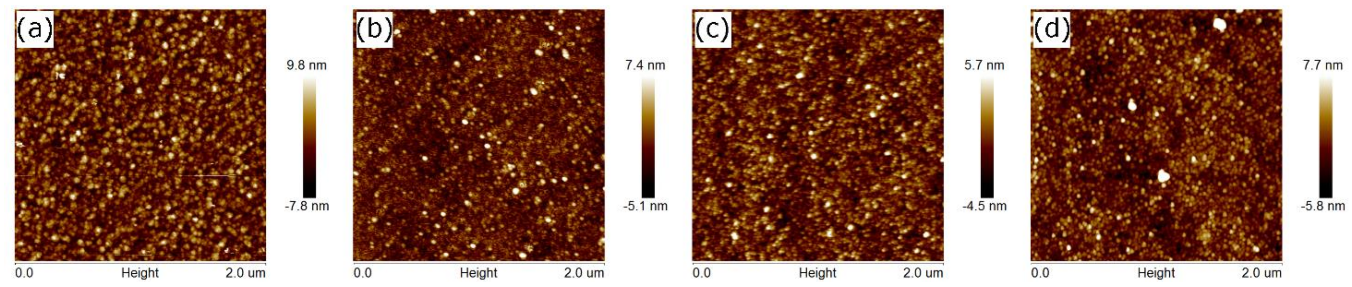
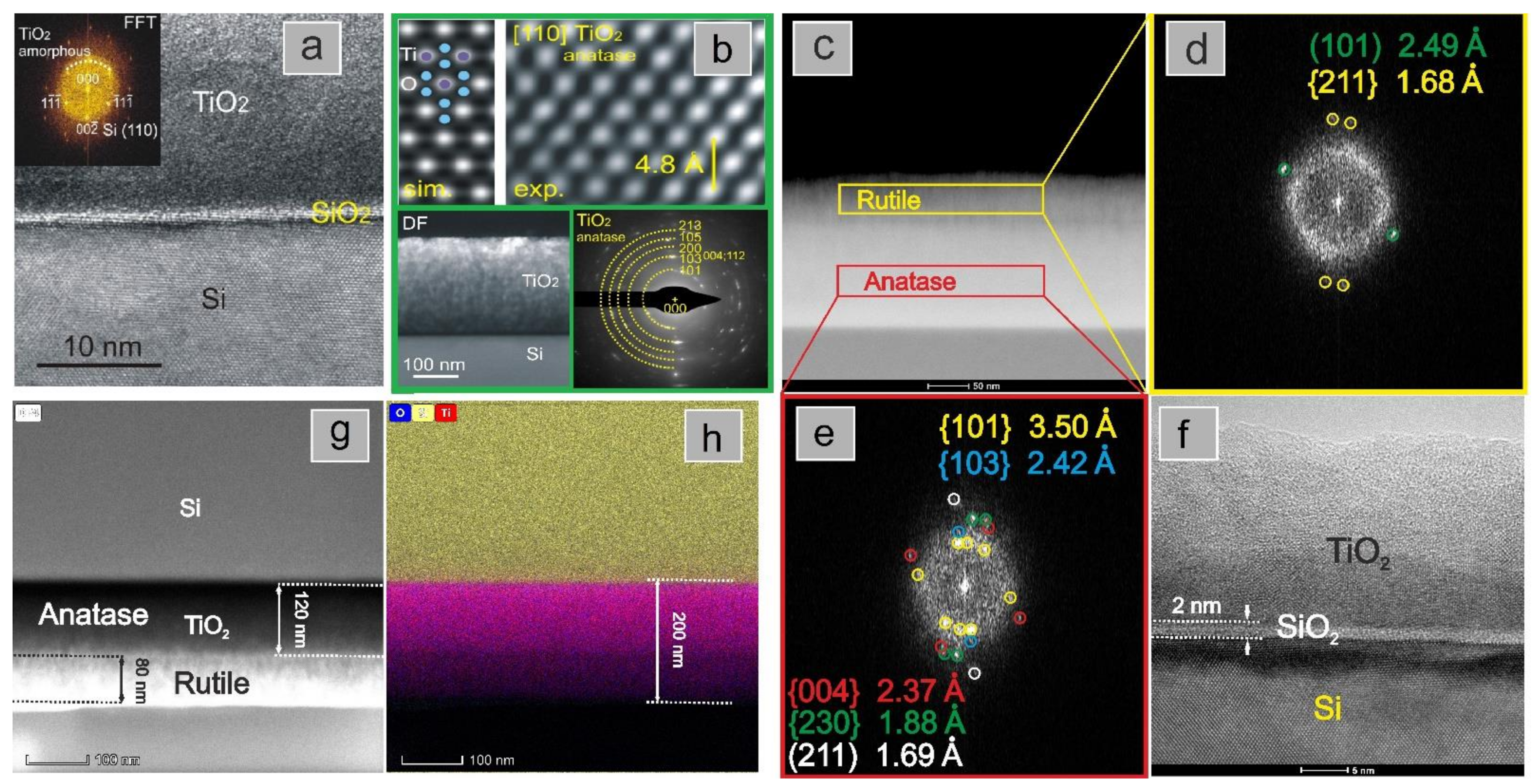
| No. | Sample | dr | d1 | d2 | Ra | Rq | <D> | <D> |
|---|---|---|---|---|---|---|---|---|
| (nm) | (nm) | (nm) | (nm) | (nm) | (nm) | (nm) | ||
| 1. | S1 | 2.3 ± 0.2 | 234 ± 1 | - | 2.0 | 2.6 | - | - |
| 2. | S1_2h | 0.6 ± 0.2 | 223 ± 1 | - | 0.8 | 1.0 | 32 ± 3 1 | 22 ± 2 2 |
| 3. | S1_2h_O2 | 0.8 ± 0.2 | 231 ± 1 | - | 1.4 | 1.7 | 25 ± 3 1 | 21 ± 2 2 |
| 4. | S1_12h | 0.8 ± 0.2 | 224 ± 1 | - | 1.2 | 1.5 | 32 ± 3 1 | 21 ± 2 2 |
| 5. | S1_12h_O2 | 0.5 ± 0.2 | 222 ± 1 | - | 1.1 | 1.4 | 25 ± 3 1 | 20 ± 2 2 |
| 6. | S2 | 2.9 ± 0.2 | 78 ± 1 | 115 ± 1 | 1.3 | 1.7 | 29 ± 3 1 | 5 ± 4 3 |
| 7. | S2_2h | 1.9 ± 0.3 | 77 ± 1 | 101 ± 1 | 1.7 | 1.5 | 41 ± 4 1 | 19 ± 2 3 |
| 8. | S2_2h_O2 | 2.8 ± 0.2 | 75 ± 1 | 108 ± 1 | 1.4 | 2.0 | 30 ± 3 1 | 19 ± 2 3 |
| 9. | S2_12h | 1.9 ± 0.2 | 78 ± 1 | 99 ± 1 | 1.2 | 1.6 | 41 ± 4 1 | 20 ± 2 3 |
| 10. | S2_12h_O2 | 2.2 ± 0.2 | 73 ± 1 | 105 ± 1 | 1.1 | 1.4 | 33 ± 3 1 | 17 ± 2 3 |
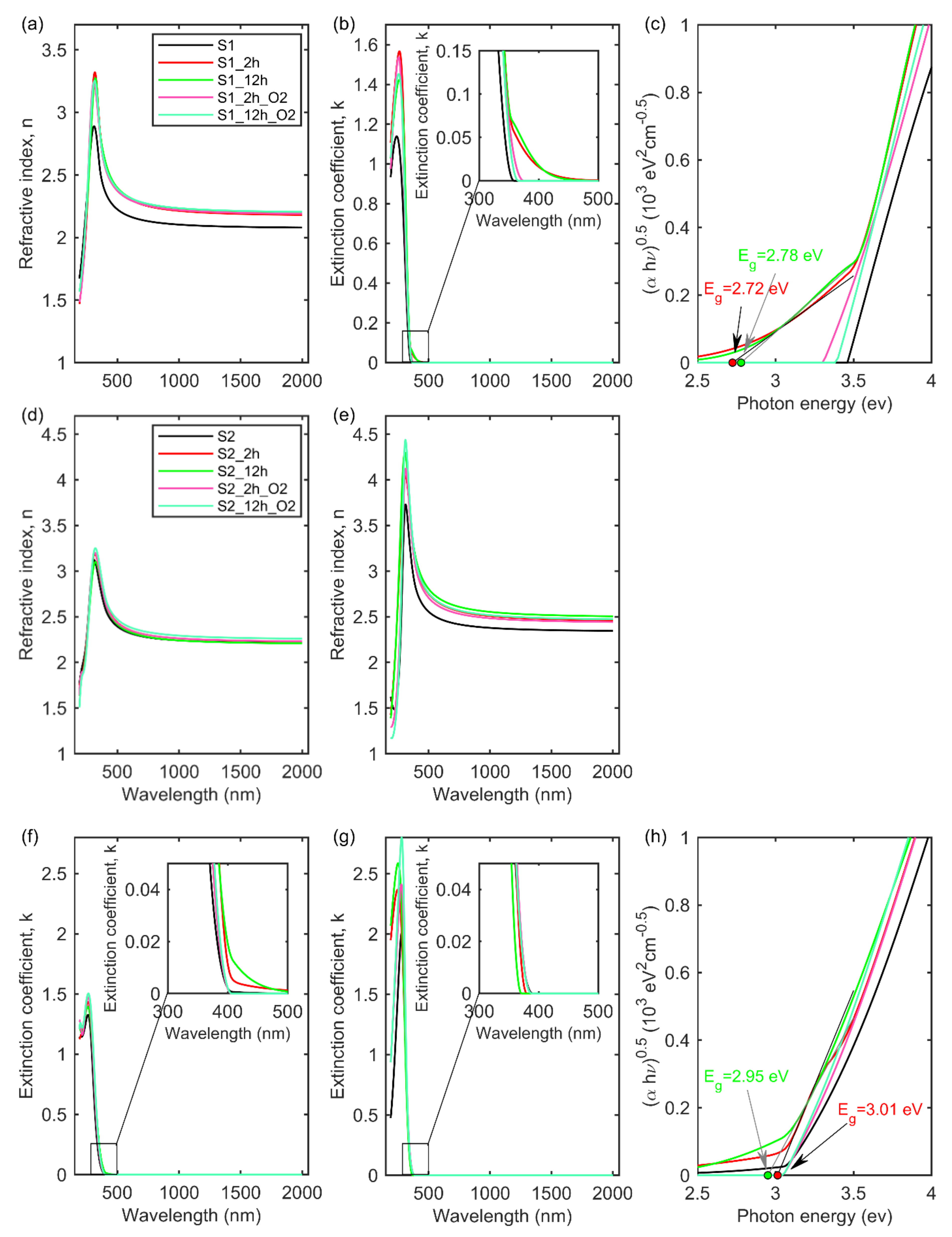
| No. | Sample | Eg1 | Eg2 | EgT-L | |||
|---|---|---|---|---|---|---|---|
| (eV) | (nm) | (eV) | (nm) | (eV) | (nm) | ||
| 1. | S1 | 3.46 ± 0.01 | 358 ± 1 | - | - | - | - |
| 2. | S1_2h | 3.47 ± 0.01 | 357 ± 1 | - | - | 2.72 ± 0.05 | 456 ± 9 |
| 3. | S1_2h_O2 | 3.31 ± 0.01 | 375 ± 1 | - | - | - | - |
| 4. | S1_12h | 3.50 ± 0.01 | 354 ± 1 | - | - | 2.78 ± 0.05 | 446 ± 8 |
| 5. | S1_12h_O2 | 3.39 ± 0.01 | 366 ± 1 | - | - | - | - |
| 6. | S2 | 3.18 ± 0.03 | 390 ± 4 | 3.05 ± 0.05 | 407 ± 7 | - | - |
| 7. | S2_2h | 3.27 ± 0.03 | 379 ± 4 | 3.05 ± 0.07 | 407 ± 10 | 3.01 ± 0.05 | 412 ± 7 |
| 8. | S2_2h_O2 | 3.20 ± 0.04 | 387 ± 5 | 3.05 ± 0.06 | 407 ± 8 | - | - |
| 9. | S2_12h | 3.35 ± 0.02 | 370 ± 3 | 3.04 ± 0.04 | 408 ± 6 | 2.95 ± 0.05 | 420 ± 8 |
| 10. | S2_12h_O2 | 3.20 ± 0.03 | 387 ± 4 | 3.05 ± 0.04 | 407 ± 6 | - | - |
Publisher’s Note: MDPI stays neutral with regard to jurisdictional claims in published maps and institutional affiliations. |
© 2021 by the authors. Licensee MDPI, Basel, Switzerland. This article is an open access article distributed under the terms and conditions of the Creative Commons Attribution (CC BY) license (https://creativecommons.org/licenses/by/4.0/).
Share and Cite
Jurek, K.; Szczesny, R.; Trzcinski, M.; Ciesielski, A.; Borysiuk, J.; Skowronski, L. The Influence of Annealing on the Optical Properties and Microstructure Recrystallization of the TiO2 Layers Produced by Means of the E-BEAM Technique. Materials 2021, 14, 5863. https://doi.org/10.3390/ma14195863
Jurek K, Szczesny R, Trzcinski M, Ciesielski A, Borysiuk J, Skowronski L. The Influence of Annealing on the Optical Properties and Microstructure Recrystallization of the TiO2 Layers Produced by Means of the E-BEAM Technique. Materials. 2021; 14(19):5863. https://doi.org/10.3390/ma14195863
Chicago/Turabian StyleJurek, Katarzyna, Robert Szczesny, Marek Trzcinski, Arkadiusz Ciesielski, Jolanta Borysiuk, and Lukasz Skowronski. 2021. "The Influence of Annealing on the Optical Properties and Microstructure Recrystallization of the TiO2 Layers Produced by Means of the E-BEAM Technique" Materials 14, no. 19: 5863. https://doi.org/10.3390/ma14195863
APA StyleJurek, K., Szczesny, R., Trzcinski, M., Ciesielski, A., Borysiuk, J., & Skowronski, L. (2021). The Influence of Annealing on the Optical Properties and Microstructure Recrystallization of the TiO2 Layers Produced by Means of the E-BEAM Technique. Materials, 14(19), 5863. https://doi.org/10.3390/ma14195863