
Physical and Dielectric Properties of Ni-Doped In2S3 Powders for Optical Windows in Thin Film Solar Cells
by
 ,
,
Abdelmajid Timoumi
1,*, 
Walid Belhadj
1,
Salah Noaiman Alamri
2 and
Mohamed Khalil Al-Turkestani
1 1
Physics Department, Faculty of Applied Science, Umm AL-Qura University, Makkah P.O. Box 715, Saudi Arabia
2
Physics Department, Faculty of Science, Taibah University, Madinah P.O. Box 30002, Saudi Arabia
*
Author to whom correspondence should be addressed.
Materials 2021, 14(19), 5779; https://doi.org/10.3390/ma14195779
Submission received: 19 August 2021
/
Revised: 25 September 2021
/
Accepted: 26 September 2021
/
Published: 3 October 2021
(This article belongs to the Section Metals and Alloys)
Abstract
:This paper reports the effect of Nickel (Ni) on indium sulfide (In2S3) powder. This work presents a systematic study of the physical and dielectric properties of In2-xS3Nix powders with 0, 2, 4, and 6 at.% of nickel. Doped and undoped samples were investigated by X-ray powder diffraction (XRD), energy dispersive X-ray spectroscopy, thermal gravimetric analysis, Fourier transform infrared (FTIR) spectroscopy, Raman spectroscopy, scanning electron microscopy (SEM), and impedance spectroscopy. XRD patterns revealed that each In2-xS3Nix composition was crystalline, which was also confirmed by the FTIR results. The presence of Ni in the samples was confirmed by energy dispersive spectroscopy (EDS). The Raman studies show different peaks related to the In2S3 phase and do not reveal any secondary phases of In–Ni and Ni–S. The SEM images of the undoped and Ni-doped In2S3 samples indicated a correlation between dopant content and the surface roughness and porosity of the samples. The impedance analysis indicated semiconductor behavior present in all samples, as well as a decrease in resistance with increasing Ni content. This work opens up the possibility of tailoring the properties and integrating Ni-doped In2S3 nanocomposites as thin film layers in future solar cells.
1. Introduction
The inorganic compound indium sulfide (In2S3) recently gained considerable attention as an optical window material in solar photovoltaic cells. In2S3 is as well non-toxic and more environmentally friendly compared to other optical window materials such as cadmium sulfide (CdS). In addition, In2S3 is an n-type semiconductor that crystallizes at atmospheric pressure in three polymorphic forms (named α, β, and γ) as a function of temperature [1]. These remarkable characteristics of In2S3 combined with its eco-friendly nature [2,3] make it well-suited for use in a variety of applications that are fabricated by different processing methods [4,5,6,7]. In2S3 is generally used in photovoltaic applications [8], semiconductor batteries [9], and photoelectrochemical cells [10,11]. Our previous research [12,13,14,15,16,17,18,19,20] included detailed investigations of several materials, including thin film indium sulfide. The latter is synthesized in our laboratory and then deposited in the form of thin layers by various techniques such as vacuum thermal evaporation and pyrolysis spray. Various theoretical and experimental studies are made depending on the effect of annealing, temperature, and doping.
In fact, some of the synthesis methods used in our research are relatively complex to manipulate, and a few are costly and time-consuming. Besides our own studies, many other researchers are interested in investigating In2S3 powders [21,22]. Hamici M. et al. [21] studied the oxidation process of the crystalline powder of In2S3 and thin films obtained by the Dr. Blade Method. They obtained samples showing a band gap varying continuously between 1.94 eV and 3.72 eV and films of intermediate composition. Gorai S. et al. [22] synthesized the In2S3 powder and studied its optical characterization and estimated a band gap value around ~2.12 eV. Other studies [23] are also carried out on CdS powder, it having physical properties close to that of In2S3 and which can be used as a thin film for solar cells.
Recently, 3D transition metal impurities in semiconductor nanoparticles attracted significant interest because of their effect on tuning the emission bands [24,25]. A study of commercially doped In2S3 will provide an alternative approach for understanding the energy-related applications of this material. In addition, commercial In2S3 powder is inexpensive and provides similar encouraging results as laboratory synthesized powders.
In this research, we investigated the effects of doping not only on the structural, morphological, and thermal properties, but also on the dielectric properties of Ni-doped and undoped In2S3 powders. The obtained results are presented and discussed below. To our knowledge, this is the first work on In2S3 powder doped with nickel.
2. Materials and Methods
2.1. Materials
In2S3, a red powder with 99.99% purity, was supplied by the Sigma-Aldrich company and used without purification. Nickel powder (Pulver, Atom Gew. 58.71) in concentrations of 2, 4, and 6 at.% was used to dope In2S3. The choice of these concentrations is estimated from our previous work, and, generally, there is a limit to the amount of dopant that could be applied. Each sample consisted of 0.2 g of In2S3. To characterize the electrical properties, the total quantity of each sample was pressed into a pellet 13 mm in diameter and 1 mm thick. Two silver paste electrodes were placed on both sides of the pellet and were connected to copper wires.
2.2. Experimental Methods
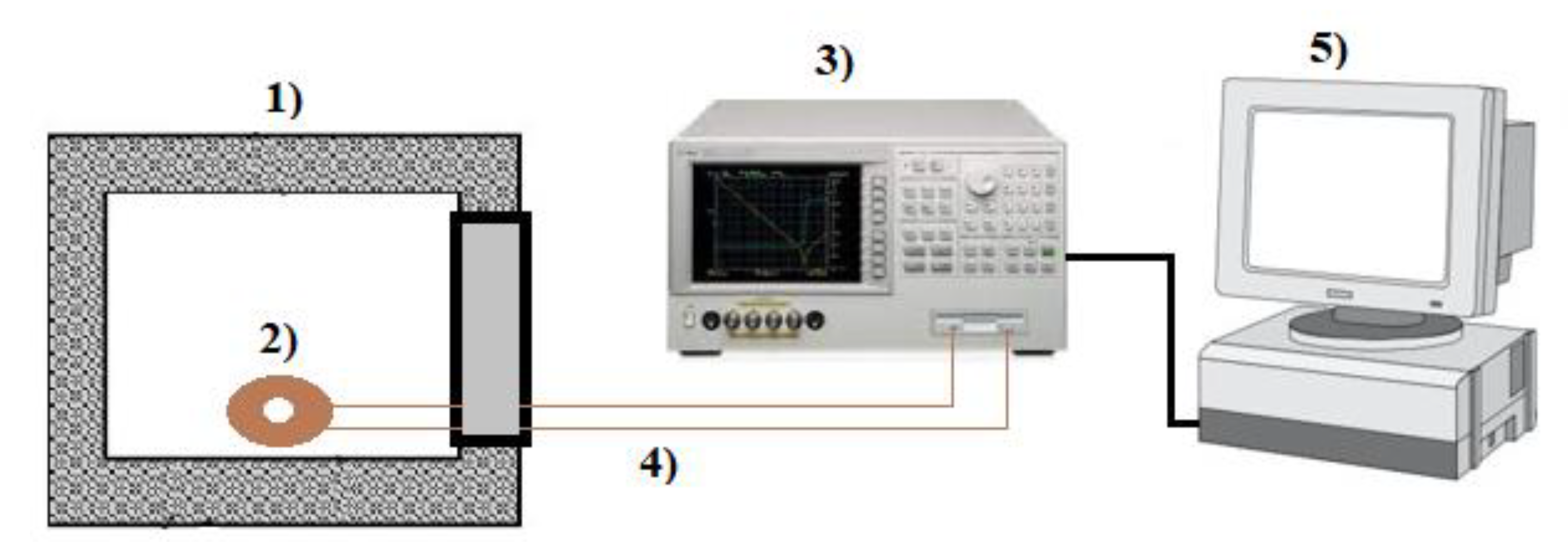
To characterize the structural properties of the In2-xS3Nix powder, we used X-Ray diffraction (XRD; Cu-Kα = 1.5418 Å, Shimadzu XRD-6000, Shimadzu, Kyoto, Japan). A thermogravimetric analysis (TGA) was performed on the undoped sample employing a TGA-1000 analyzer (Navas Instruments, Conway, SC, USA). Scanning Electron microscopy (SEM; Supers can SSX-550, Shimadzu, Japan) was used to analyze the surface morphology of the samples. To investigate the crystal phases, we used Raman spectroscopy (RS; 532 nm laser, Senterra, Bruker, Billerica, MA, USA). The complex impedance parameters were investigated as a function of frequency (10 Hz–13 MHz) using a computer-controlled impedance analyzer (Agilent 4294A, Agilent, Santa Clara, CA, USA). The entire experimental system is shown in Figure 1.
3. Results and Discussion
3.1. XRD and EDS Analysis
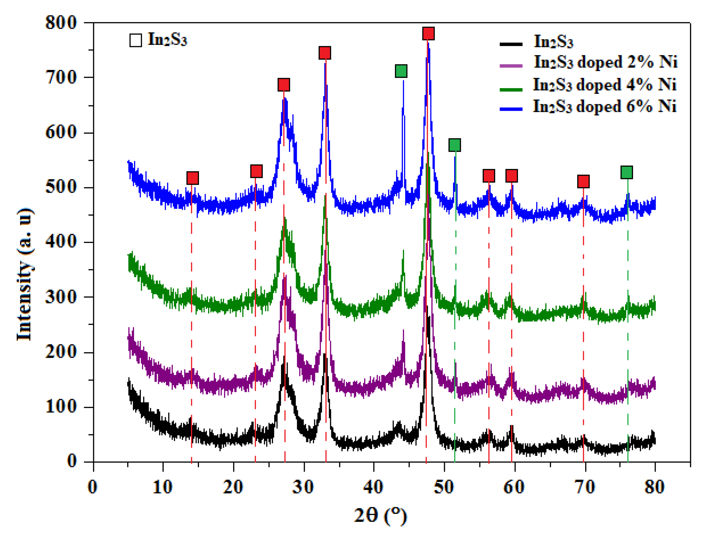
X-ray diffraction (Cu–Kα = 1.5418 Å) was used to analyze the structures of the In2S3 and In2-xS3Nix samples. Figure 2 shows that all samples were crystalline. This result agrees with that obtained by Lucena et al. [26]. The appearance of other peaks is also apparent depending on the increase in the dopant level at 2θ angles of 44°, 52°, and 77°, as indicated by the green squares in Figure 2. These peaks are most likely the residual stress in the sample caused by the difference in ionic size between Ni2+ (0.70 Å) and In3+ (0.80 Å) [27]. No other phase corresponding to the nickel impurity was detected, which is explained by the fact that the Ni ions occupy sulfur substitution positions and do not change the crystal system of the material.
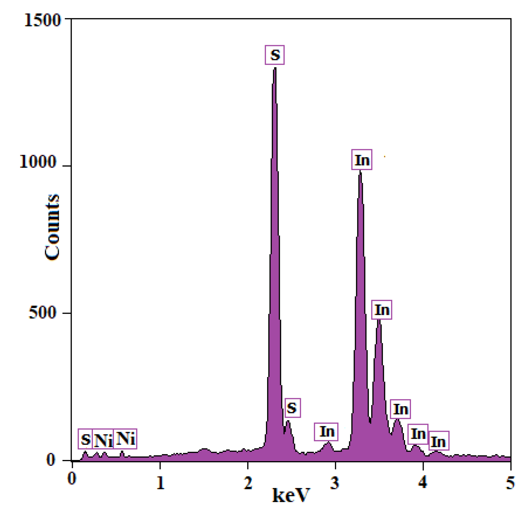
A compositional analysis was performed using energy-dispersive X-ray spectroscopy (EDS). The EDS pattern of the undoped In2S3 samples (Figure 3) shows the presence of indium and sulfur elements in an atomic percentage ratio of 2/3 for In:S. The other unidentified peaks were attributed to the glass substrate.
The EDS analysis also confirmed the presence of different nickel contents for each sample. The atomic percentages of the elements in the samples are listed in Table 1, which indicates that when the Ni content increased, the quantity of indium decreased slightly, and the percentage of sulfur remained constant. It is expected that Ni doping of the In2S3 samples was substitutional.
3.2. Thermal Analysis
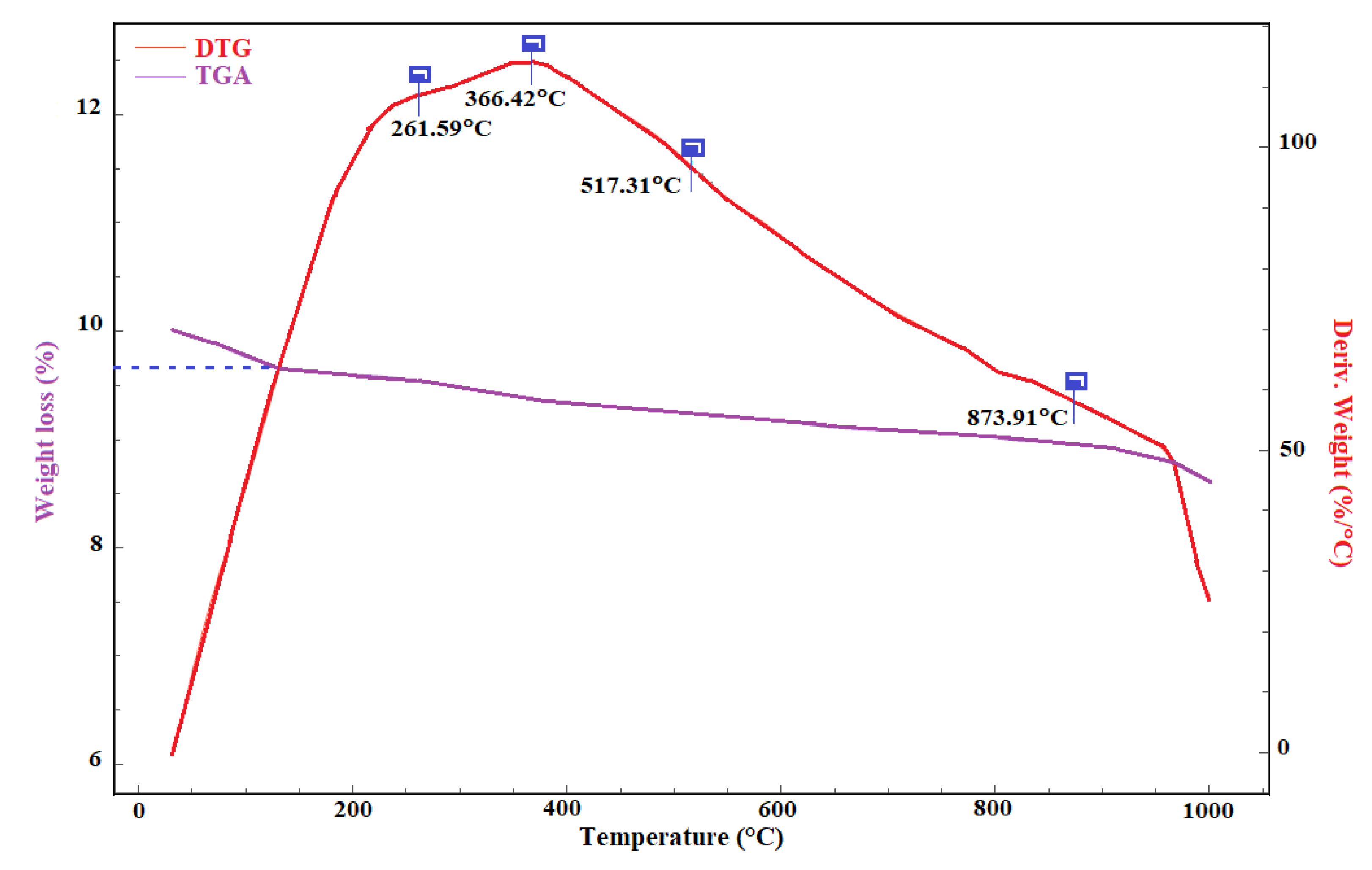
The thermal behavior of the In2S3 material was studied using a TGA. As shown in Figure 4, the TGA thermograms show that the untreated In2S3 material is thermally stable at temperatures beyond 400 °C, and the weight loss is approximately 5%. This behavior is attributed to the purity and crystallinity of the material.
3.3. Raman Analysis
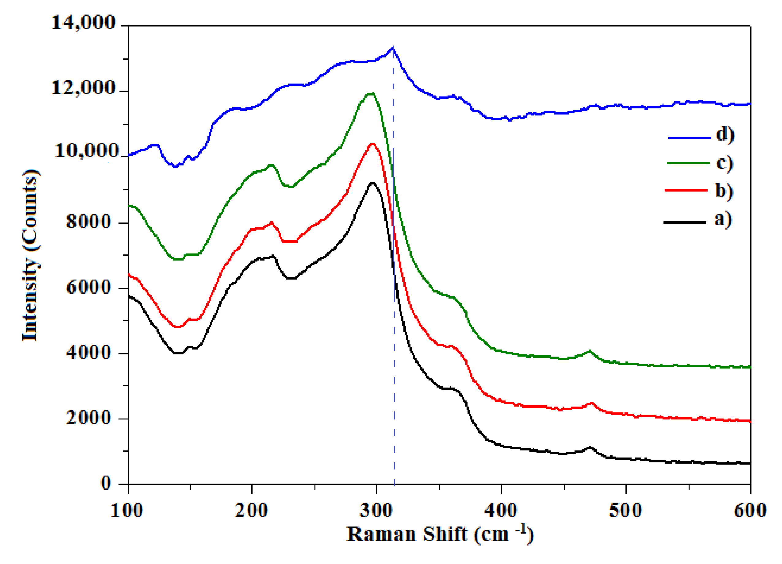
Figure 5 presents the experimental Raman spectra for all samples in the range 100–600 cm−1, which indicates the presence of In2S3 phase modes, in agreement with the results obtained by Kraini et al. [28]. The active modes were observed at 115, 210, 308, and 365 cm−1, confirming their composition and structure [29]. The indicated modes produced broad peaks with low intensity. At about 220 cm−1, the observed peak corresponds to the presence of elemental sulfur in the structure of the thin film. At near 300 cm−1, the obtained Raman mode is attributed to the Eg mode of the In–S bond. The position of the peak and the half-width of the phase of Raman bands were independent of the Ni-doping content. However, there was a slight change in the relative intensity of the Raman band at 315 cm−1, which appears to correlate with the changes observed by X-ray diffraction for the sample containing 6 at.% Ni. We also noticed the absence of secondary phases, which is in good agreement with the obtained XRD results.
3.4. FTIR
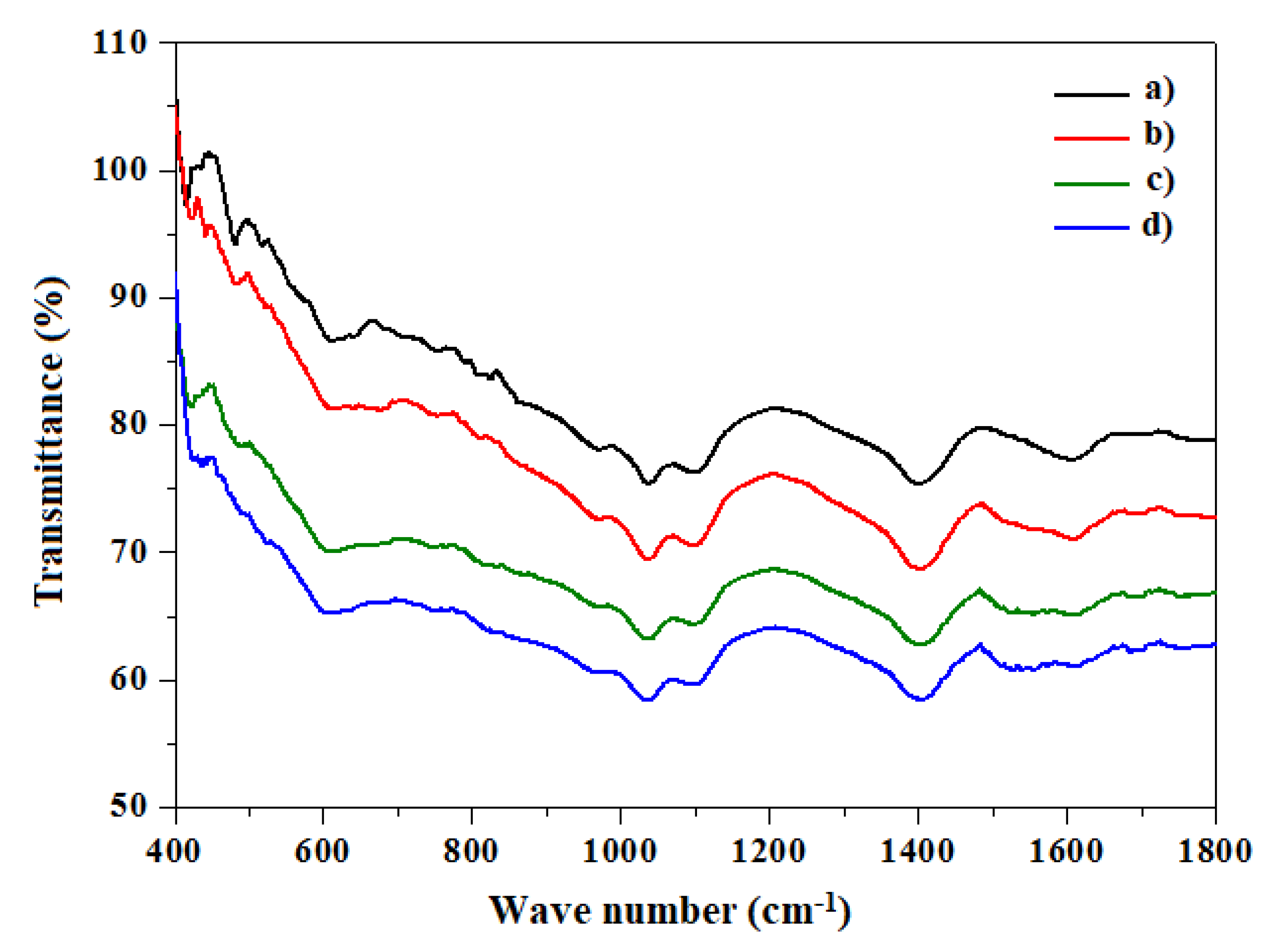
FTIR spectral fingerprints for each sample in the wavenumber range of 100 to 600 cm−1 provided details of the chemical structure. Figure 6 shows the presence of three absorption bands at 1000–1500 cm−1 corresponding to the extension of the C–H and O–H bonds, and also at 900–1200 cm−1 and approximately 800 cm−1 corresponding to the stretching of the C=O bonds and the O–H band, respectively.
3.5. SEM
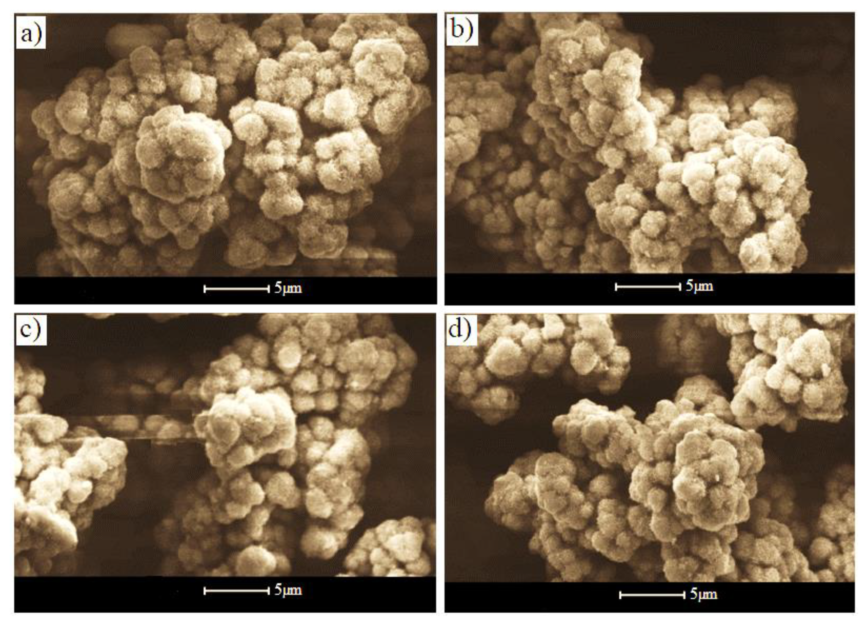
Figure 7 shows the SEM images of the undoped In2S3 and Ni-doped In2S3 samples. The surfaces show highly irregular surface roughness and porosity that increase with increasing the Ni-doping concentration, as shown in Figure 7d. There was also a clear increase in the number of grains with increasing Ni content, as well as surface homogeneity. This is probably due to Ni filling the pores on the surface of the composite layer. From the SEM images, the surface roughness obviously increased after doping.
3.6. Electrical Impedance
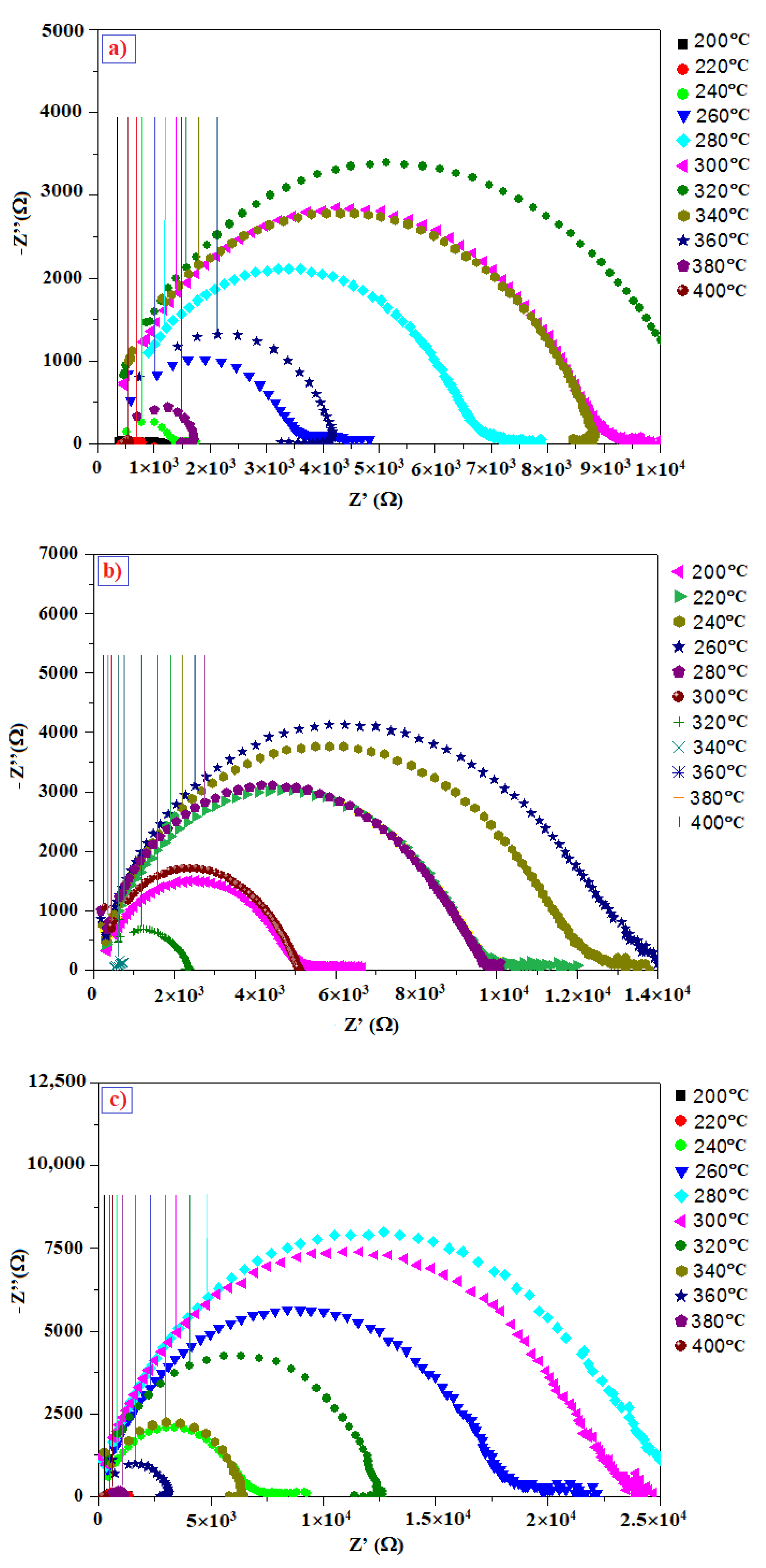
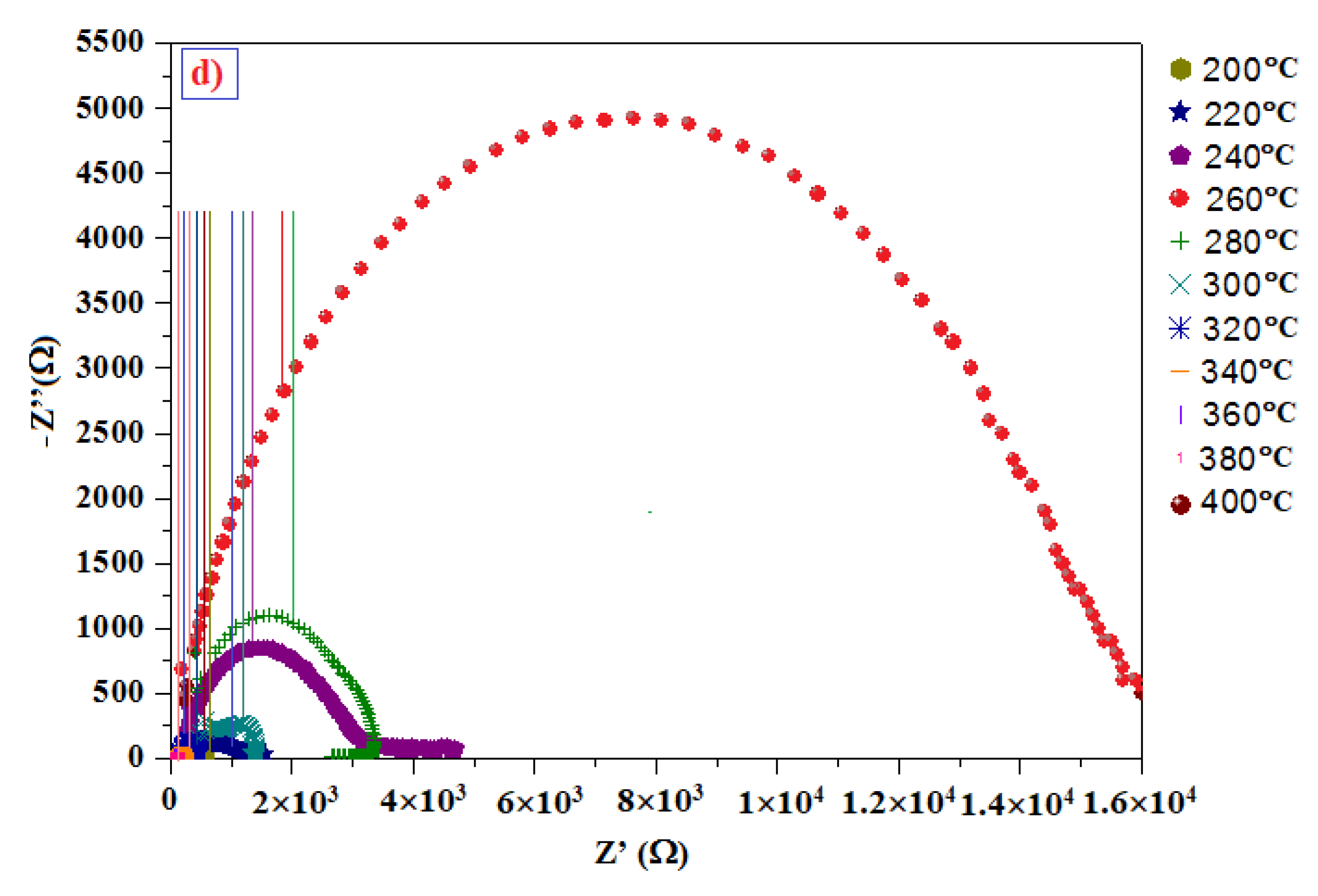
Currently, much work is interested in electrical and dielectric properties of materials [30,31,32]. Nyquist plots are commonly used for characterizing electrical and dielectric properties of semiconductors’ materials [33,34,35,36], so we constructed Nyquist plots for our In2S3 powder samples. Doping is one of the approaches used to minimize electrical resistivity [37]; therefore, to study the dopant effects on the dielectric behavior of the In2S3 samples, we used impedance spectroscopy (IS). The undoped and doped In2S3 powders were pressed into a pellet (13 mm diameter and 1 mm thickness) prior to applying silver paste, which served as an electrical contact. The Nyquist plots obtained for all samples in the frequency range of 10 Hz to 30 MHz and at different temperatures of 200–400 °C are presented in Figure 8. These Nyquist plots exhibit semi-circular arcs whose centers are located under the real part axis, which suggests a non-Debye-type relaxation phenomenon of the charge carriers [38]. The diameter and shape of the semicircles changed with the temperature, which indicates temperature-dependent semiconductor behavior [39,40]. Initially, the Nyquist diagrams illustrate increases in the semi-circular diameters as the temperature increases above 200 °C [33,41]. However, the semi-circles shifted to lower frequencies, and their diameters decreased after heating to 260–320 °C, indicating a thermally activated electrical conductivity and relaxation time distribution [42]. This phenomenon was observed at 320 °C for pure In2S3 and from 280 °C to 260 °C for the Ni-doped samples. Resistance values decreased rapidly with temperature, and the carrier concentration increased with doping because indium sulfide has many vacant indium sites [43].
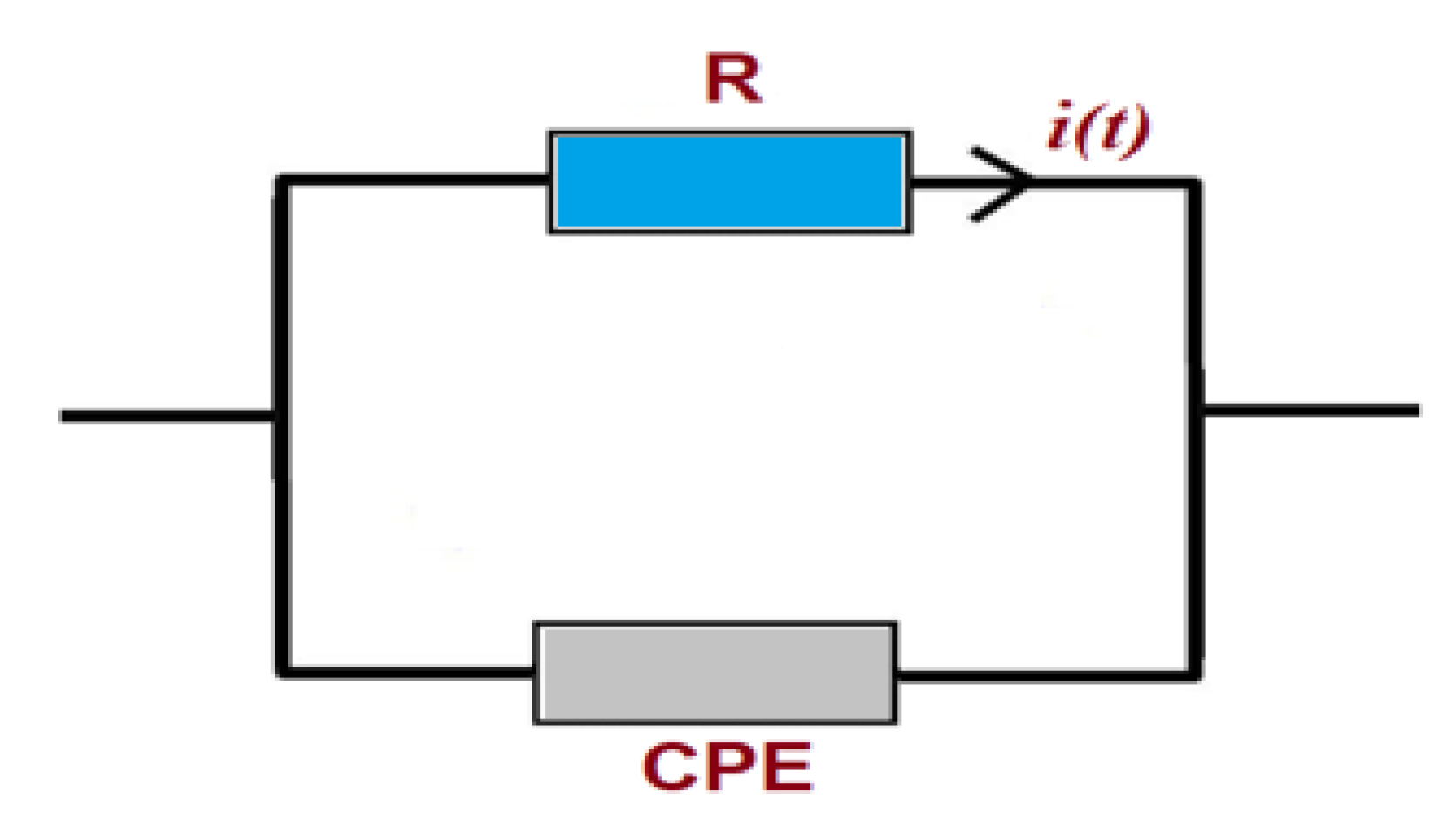
The modeling of the measured impedance spectra and the choice of an appropriate electrical equivalent circuit allow us to consider the electrical phenomena in our undoped and Ni-doped In2S3 material. The ZSimpWin 3.10 program was used to compute the circuit parameters. The assigned equivalent circuit for this study is shown in Figure 9, in which the resistance is connected in parallel to the constant phase element impedance (CPE).
Q is a constant value independent of frequency; Ω is the angular frequency; and β is an exponent that measures the arc depression of the CPE impedance [45].
4. Conclusions
In summary, we investigated the effect of doping In2S3 powder with nickel on the crystal structure, distribution of dopants, thermal behavior, molecular structure and bonding modes, surface morphology, and electrical impedance. This study showed that Ni doping preserved the crystallinity of each dopant concentration, and no phase changes were observed due to Ni doping. The EDS analysis proved that the In2S3 samples had a Ni-rich and S-deficient composition. The SEM images presented in this work showed a gradual formation of dense samples that were free of cracks with increasing Ni content. The electrical conductance improved with increasing the temperature from a certain characteristic value of the sample. The results obtained in this study highlight the significant effect of doping on the electrical and structural properties of In2S3 especially in its powder form. The results reported in this study may facilitate the use of In2S3 materials for future applications in photovoltaic devices.
Author Contributions
Conceptualization, A.T., W.B., S.N.A., M.K.A.-T.; Methodology, A.T., W.B., S.N.A., M.K.A.-T.; Data Investigation, A.T., S.N.A.; Supervision, A.T.; Visualization, A.T., W.B., S.N.A., M.K.A.-T.; Writing—Original draft, A.T.; Writing—Review and Editing, contribution by all the authors. All authors have read and agreed to the published version of the manuscript.
Funding
This research was supported by the Scientific Research (19- SCI-1-01-0013) of Umm Al-Qura University, Saudi Arabia.
Institutional Review Board Statement
Not applicable.
Informed Consent Statement
Not applicable.
Data Availability Statement
The data presented in this study are available on request from the corresponding author.
Acknowledgments
The authors would like to thank the Deanship of Scientific Research at Umm Al-Qura University for supporting this work (Grant Code: 19- SCI-1-01-0013).
Conflicts of Interest
The authors declare no conflict of interest. The funders had no role in the design of the study; in the collection, analyses, or interpretation of data; in the writing of the manuscript, or in the decision to publish the results.
References
- Revathi, N.; Prathap, P.; Miles, R.; Reddy, K.R. Annealing effect on the physical properties of evaporated In2S3 films. Sol. Energy Mater. Sol. Cells 2010, 94, 1487–1491. [Google Scholar] [CrossRef]
- Hsiao, Y.-J.; Lu, C.-H.; Ji, L.-W.; Meen, T.-H.; Chen, Y.-L.; Chi, H.-P. Characterization of photovoltaics with In2S3 nanoflakes/p-Si heterojunction. Nanoscale Res. Lett. 2014, 9, 32. [Google Scholar] [CrossRef] [PubMed] [Green Version]
- Rasool, S.; Saritha, K.; Reddy, K.R.; Bychto, L.; Patryn, A.; Maliński, M.; Tivanov, M.; Gremenok, V. Optical properties of thermally evaporated In 2 S 3 thin films measured using photoacoustic spectroscopy. Mater. Sci. Semicond. Process. 2017, 72, 4–8. [Google Scholar] [CrossRef]
- Sim, Y.; Kim, J.; Chang, S.H.; Choi, C.-J.; Seong, M.-J. Highly luminescent In2S3 thin films with preferred growth direction of [1 0 3]. Appl. Surf. Sci. 2021, 555, 149706. [Google Scholar] [CrossRef]
- De Moure-Flores, F.; Nieto-Z, K.E.; Guillén, C.A.; Gallardo, S.; Quiñones, G.J.G.; Hernández, H.A.; Olvera, L.M.; Zapata, T.M.; Kundriavtsev, Y.; Meléndez, L.M. Effect of the immersion in CdCl2 and annealing on physical properties of CdS:F films grown by CBD. J. Phys. Chem. Solids 2013, 74, 611. [Google Scholar] [CrossRef]
- Hashemi, M.; Heidariramsheh, M.; Ghorashi, S.M.B.; Taghavinia, N.; Mahdavi, S.M. Study on spray-pyrolyzed In2S3 thin films, targeted as electron transport layer in solar energy. J. Photon-Energy 2020, 10, 024001. [Google Scholar] [CrossRef]
- Gao, W.; Liu, W.; Leng, Y.; Wang, X.; Wang, X.; Hu, B.; Yu, D.; Sang, Y.; Liu, H. In2S3 nanomaterial as a broadband spectrum photocatalyst to display significant activity. Appl. Catal. B Environ. 2015, 176–177, 83–90. [Google Scholar] [CrossRef]
- Sarkar, S.K.; Kim, J.Y.; Goldstein, D.N.; Neale, N.R.; Zhu, K.; Elliott, C.M.; Frank, A.J.; George, S.M. In2S3 atomic layer deposition and its application as a sensitizer on TiO2 nanotube arrays for solar energy conversion. J. Phys. Chem. C 2010, 114, 17, 8032. [Google Scholar] [CrossRef]
- Nehra, S.; Chander, S.; Sharma, A.; Dhaka, M. Effect of thermal annealing on physical properties of vacuum evaporated In2S3 buffer layer for eco-friendly photovoltaic applications. Mater. Sci. Semicond. Process. 2015, 40, 26–34. [Google Scholar] [CrossRef]
- Pulipaka, S.; Koushik, A.K.S.; Deepa, M.; Meduri, P. Enhanced photoelectrochemical activity of Co-doped β-In2S3nanoflakes as photoanodes for water splitting. RSC Adv. 2019, 9, 1335–1340. [Google Scholar] [CrossRef] [Green Version]
- Kwoka, M.; Ottaviano, L.; Szuber, J. AFM study of the surface morphology of L-CVD SnO2 thin films. Thin Solid Film. 2007, 515, 8328–8331. [Google Scholar] [CrossRef]
- Timoumi, A.; Bouzouita, H.; Kanzari, M.; Rezig, B. Fabrication and characterization of In2S3 thin films deposited by thermal evaporation technique. Thin Solid Films 2005, 480–481, 124–128. [Google Scholar] [CrossRef]
- Timoumi, A.; Bouzouita, H.; Brini, R.; Kanzari, M.; Rezig, B. Optimization of annealing conditions of In2S3 thin films deposited by vacuum thermal evaporation. Appl. Surf. Sci. 2006, 253, 306–310. [Google Scholar] [CrossRef]
- Timoumi, A.; Bouzouita, H.; Rezig, B. Optical constants of Na–In2S3 thin films prepared by vacuum thermal evaporation technique. Thin Solid Film. 2011, 519, 7615–7619. [Google Scholar] [CrossRef]
- Bouguila, N.; Timoumi, A.; Bouzouita, H.; Lacaze, E.; Bouchriha, H.; Rezig, B. Molar ratio S/In effect on properties of sprayed In2S3films. Eur. Phys. J. Appl. Phys. 2013, 63, 20301. [Google Scholar] [CrossRef]
- Bouguila, N.; Timoumi, A.; Bouzouita, H. Vacuum annealing temperature on spray In2S3layers. Eur. Phys. J. Appl. Phys. 2014, 65, 20304. [Google Scholar] [CrossRef]
- Bouguila, N.; Kraini, M.; Timoumi, A.; Halidou, I.; Vazquez-Vazquez, C.; López-Quintela, M.A.; Alaya, S. Substrate temperature effect on properties of sprayed In2S3 films. J. Mater. Sci. Mater. Electron. 2015, 26, 7639–7648. [Google Scholar] [CrossRef]
- Timoumi, A.; Bouguila, N.; Chaari, M.; Kraini, M.; Matoussi, A.; Bouzouita, H. Electrical and dielectric properties of In2S3 synthesized by solid state reaction. J. Alloys Compd. 2016, 679, 59–64. [Google Scholar] [CrossRef]
- Abassi, H.; Bouguila, N.; Timoumi, A. Theoretical Study of the AC Conduction in β-In2S3. J. Electron. Mater. 2018, 47, 2519–2525. [Google Scholar] [CrossRef]
- Timoumi, A.; Belhadj, W.; Alamri, S.; Al Turkestani, M. Experimental studies and new theoretical modeling on the properties of In2S3 thin films. Opt. Mater. 2021, 118, 111238. [Google Scholar] [CrossRef]
- Hamici, M.; Guessoum, K.; Vaillant, L.; Gagou, Y.; Saint-Grégoire, P. Study of the Oxidation Process of Crystalline Powder of In2S3 and Thin Films Obtained by Dr Blade Method. J. Electron. Mater. 2019, 48, 4715–4725. [Google Scholar] [CrossRef] [Green Version]
- Gorai, S.; Guha, P.; Ganguli, D.; Chaudhuri, S. Chemical synthesis of β-In2S3 powder and its optical characterization. Mater. Chem. Phys. 2003, 82, 974–979. [Google Scholar] [CrossRef]
- Alamri, S.N. Structure and optical properties of chunk and powder CdS film prepared by electron beam deposition. Indian J. Phys. 2013, 88, 259–264. [Google Scholar] [CrossRef]
- Masikane, S.C.; McNaughter, P.D.; Lewis, D.J.; Vitorica-Yrezabal, I.; Doyle, B.P.; Carleschi, E.; O’Brien, P.; Revaprasadu, N. Important Phase Control of Indium Sulfide Nanomaterials by Choice of Indium(III) Xanthate Precursor and Thermolysis Temperature. Eur. J. Inorg. Chem. 2019, 2019, 1421–1432. [Google Scholar] [CrossRef]
- Ghosh, S.; Saha, M.; Ashok, V.D.; Chatterjee, A.; De, S.K. Excitation dependent multicolor emission and photoconductivity of Mn, Cu doped In2S3monodisperse quantum dots. Nanotechnology 2016, 27, 155708. [Google Scholar] [CrossRef] [PubMed]
- Lucena, R.; Conesa, J.C.; Aguilera, I.; Palacios, P.; Wahnón, P. V-substituted In2S3: An intermediate band material with photocatalytic activity in the whole visible light range. J. Mater. Chem. A 2014, 2, 8236–8245. [Google Scholar] [CrossRef] [Green Version]
- Timoumi, A.; Zayoud, W.; Sharma, A.; Kraini, M.; Bouguila, N.; Hakamy, A.; Revaprasadu, N.; Alaya, S. Impact of thermal annealing inducing oxidation process on the crystalline powder of In2S3. J. Mater. Sci. Mater. Electron. 2020, 31, 13636–13645. [Google Scholar] [CrossRef]
- Kraini, M.; Bouguila, N.; Moutia, N.; El Ghoul, J.; Khirouni, K.; Vázquez-Vázquez, C. Properties of nickel doped In2S3 thin films deposited by spray pyrolysis technique. J. Mater. Sci. Mater. Electron. 2017, 29, 1888–1906. [Google Scholar] [CrossRef]
- Aldon, L.; Uhrmacher, M.; Branci, C.; Ziegler, L.; Roth, J.; Schaaf, P.; Metzner, H.; Olivier, F.J.; Jumas, J.C. Perturbed angular correlation study of the thiospinel β−In2S3. Phys. Rev. B. 1998, 58, 11303. [Google Scholar] [CrossRef]
- Liu, P.; Ng, V.M.H.; Yao, Z.; Zhou, J.; Lei, Y.; Yang, Z.; Lv, H.; Kong, L.B. Facile Synthesis and Hierarchical Assembly of Flowerlike NiO Structures with Enhanced Dielectric and Microwave Absorption Properties. ACS Appl. Mater. Interfaces 2017, 9, 16404–16416. [Google Scholar] [CrossRef] [PubMed]
- Liu, P.; Yao, Z.; Zhou, J.; Yang, Z.; Kong, L.B. Small magnetic Co-doped NiZn ferrite/graphene nanocomposites and their dual-region microwave absorption performance. J. Mater. Chem. C 2016, 4, 9738–9749. [Google Scholar] [CrossRef]
- Liu, P.; Yao, Z.; Ng, V.M.H.; Zhou, J.; Kong, L.B.; Yue, K. Facile synthesis of ultrasmall Fe3O4 nanoparticles on MXenes for high microwave absorption performance. Compos. Part A 2018, 115, 371. [Google Scholar] [CrossRef]
- Koaib, J.; Bouguila, N.; Abassi, H.; Moutia, N.; Kraini, M.; Timoumi, A.; Vázquez-Vázquez, C.; Khirouni, K.; Alaya, S. Dielectric and electrical properties of annealed ZnS thin films. The appearance of the OLPT conduction mechanism in chalcogenides. RSC Adv. 2020, 10, 9549–9562. [Google Scholar] [CrossRef]
- Chakroun, R.; Jamoussi, B.; Al-Mur, B.; Timoumi, A.; Essalah, K. Impedance Spectroscopy and Dielectric Relaxation of Imidazole-Substituted Palladium(II) Phthalocyanine (ImPdPc) for Organic Solar Cells. ACS Omega 2021, 6, 10655–10667. [Google Scholar] [CrossRef]
- Timoumi, A.A.; Bouguila, N.; Koaib, J.; Al Turkestani, M.K.; Jamoussi, B.; Timoumi, A.; Koiab, J. Study of electrical and dielectric properties of palladium-phthalocyanine (PdPc) in pellet form. Mater. Res. Express 2019, 6, 055103. [Google Scholar] [CrossRef]
- Timoumi, A.; Wederni, M.A.; Bouguila, N.; Jamoussi, B.; AL Turkestani, M.K.; Chakroun, R.; Al-Mur, B. Electrical impedance spectroscopy study of unsubstituted palladium (II) phthalocyanine. Synth. Met. 2021, 272, 116659. [Google Scholar] [CrossRef]
- Tao, H.; Zang, H.; Dong, G.; Zeng, J.; Zhao, X. Raman and infrared spectroscopic study of the defect spinel In21.333S32. Optoelectron. Adv. Mater. 2008, 2, 356. [Google Scholar]
- Aakansha; Deka, B.; Ravi, S.; Pamu, D. Impedance spectroscopy and ac conductivity mechanism in Sm doped Yttrium Iron Garnet. Ceram. Int. 2017, 43, 10468–10477. [Google Scholar] [CrossRef]
- Khosravi, S.H.; Veerapanduyan, V.K.; Vallant, R.; Reichmann, K. Effect of processing conditions on the structural properties and corrosion behavior of TiO2–SiO2 multilayer coatings derived via the sol-gel method. Ceram. Int. 2020, 46, 17741. [Google Scholar] [CrossRef]
- Ahmad, I.; Akhtar, M.J.; Hasan, M.M. Impedance spectroscopic investigation of electro active regions, conduction mechanism and origin of colossal dielectric constant in Nd1−xSrxFeO3 (0.1 ≤ x ≤ 0.5). Mater. Res. Bull. 2014, 60, 474. [Google Scholar] [CrossRef]
- Tan, F.K.; Hassan, J.; Wahab, Z.A.; Azis, R.S. Electrical conductivity and dielectric behaviour of manganese and vanadium mixed oxide prepared by conventional solid state method. Eng. Sci. Technol. Int. J. 2016, 19, 2081–2087. [Google Scholar] [CrossRef] [Green Version]
- Trabelsi, I.; Jebali, A.; Kanzari, M. Electrical characterization of SnSb4S7 thin films by impedance spectroscopy. J. Mater. Sci. Mater. Electron. 2016, 27, 4326–4335. [Google Scholar] [CrossRef]
- Pistor, P.; Merino, Á.J.M.; León, M.; Michiel, M.; Schorr, S.; Klenk, R.; Lehmann, S. Structure reinvestigation of α-, β- and γ-In2S3. Acta Crystallogr. B. 2016, 72, 410. [Google Scholar] [CrossRef] [PubMed] [Green Version]
- Zoltowski, P. On the electrical capacitance of interfaces exhibiting constant phase element behaviour. J. Electroanal. Chem. 1998, 443, 149–154. [Google Scholar] [CrossRef]
- Jorcin, J.-B.; Orazem, M.; Pébère, N.; Tribollet, B. CPE analysis by local electrochemical impedance spectroscopy. Electrochim. Acta 2005, 51, 1473–1479. [Google Scholar] [CrossRef]
Figure 1.
Schematic diagram of experimental system: (1) furnace, (2) pellet with electrodes, (3) impedance analyzer, (4) copper wires, and (5) computer.
Figure 1.
Schematic diagram of experimental system: (1) furnace, (2) pellet with electrodes, (3) impedance analyzer, (4) copper wires, and (5) computer.

Figure 2.
XRD patterns of In2S3 and In2S3 doped with (2, 4, and 6 at.%) Ni.

Figure 3.
The EDS pattern of the undoped In2S3 powder.

Figure 4.
TGA and DTG analysis of the undoped In2S3 powder.

Figure 5.
Raman spectra of (a) undoped In2S3 and In2S3 doped with (b) 2 at.%, (c) 4 at.%, and (d) 6 at.% Ni.
Figure 5.
Raman spectra of (a) undoped In2S3 and In2S3 doped with (b) 2 at.%, (c) 4 at.%, and (d) 6 at.% Ni.

Figure 6.
FTIR spectra of (a) undoped In2S3 and In2S3 doped with (b) 2, (c) 4, and (d) 6 at.% Ni.

Figure 7.
SEM images of (a) undoped In2S3 and In2S3 doped with (b) 2, (c) 4, and (d) 6 at.% Ni.

Figure 8.
(-Z′′ vs. Z′) plots of (a) In2S3 and In2S3 doped with (b) 2, (c) 4, and (d) 6 at.% Ni and heated to 200–400 °C.
Figure 8.
(-Z′′ vs. Z′) plots of (a) In2S3 and In2S3 doped with (b) 2, (c) 4, and (d) 6 at.% Ni and heated to 200–400 °C.


Figure 9.
The proposed equivalent circuit.


Table 1.
Chemical composition of In2S3 and In2S3:Ni samples.
| Ni:In Ratio in Powder Samples | Elements | ||
|---|---|---|---|
| In (at.%) | S (at.%) | Ni (at.%) | |
| Undoped | 40.54 | 59.46 | 0 |
| 2% | 39.47 | 58.50 | 2.04 |
| 4% | 40.12 | 57.08 | 2.80 |
| 6% | 39.63 | 56.70 | 3.67 |
Publisher’s Note: MDPI stays neutral with regard to jurisdictional claims in published maps and institutional affiliations. |
© 2021 by the authors. Licensee MDPI, Basel, Switzerland. This article is an open access article distributed under the terms and conditions of the Creative Commons Attribution (CC BY) license (https://creativecommons.org/licenses/by/4.0/).
Share and Cite
MDPI and ACS Style
Timoumi, A.; Belhadj, W.; Alamri, S.N.; Al-Turkestani, M.K. Physical and Dielectric Properties of Ni-Doped In2S3 Powders for Optical Windows in Thin Film Solar Cells. Materials 2021, 14, 5779. https://doi.org/10.3390/ma14195779
AMA Style
Timoumi A, Belhadj W, Alamri SN, Al-Turkestani MK. Physical and Dielectric Properties of Ni-Doped In2S3 Powders for Optical Windows in Thin Film Solar Cells. Materials. 2021; 14(19):5779. https://doi.org/10.3390/ma14195779
Chicago/Turabian StyleTimoumi, Abdelmajid, Walid Belhadj, Salah Noaiman Alamri, and Mohamed Khalil Al-Turkestani. 2021. "Physical and Dielectric Properties of Ni-Doped In2S3 Powders for Optical Windows in Thin Film Solar Cells" Materials 14, no. 19: 5779. https://doi.org/10.3390/ma14195779
Note that from the first issue of 2016, this journal uses article numbers instead of page numbers. See further details here.