
Influence of 1.5 wt.% Bi on the Microstructure, Hardness, and Shear Strength of Sn-0.7Cu Solder Joints after Isothermal Annealing

 ,
,  ,
, 
 ,
, 
Abstract
:1. Introduction
2. Materials and Methods
3. Results
3.1. Primary Intermetallic Compound
3.2. Interfacial Intermetallic Compound and Activation Energy
3.3. Mechanical Properties
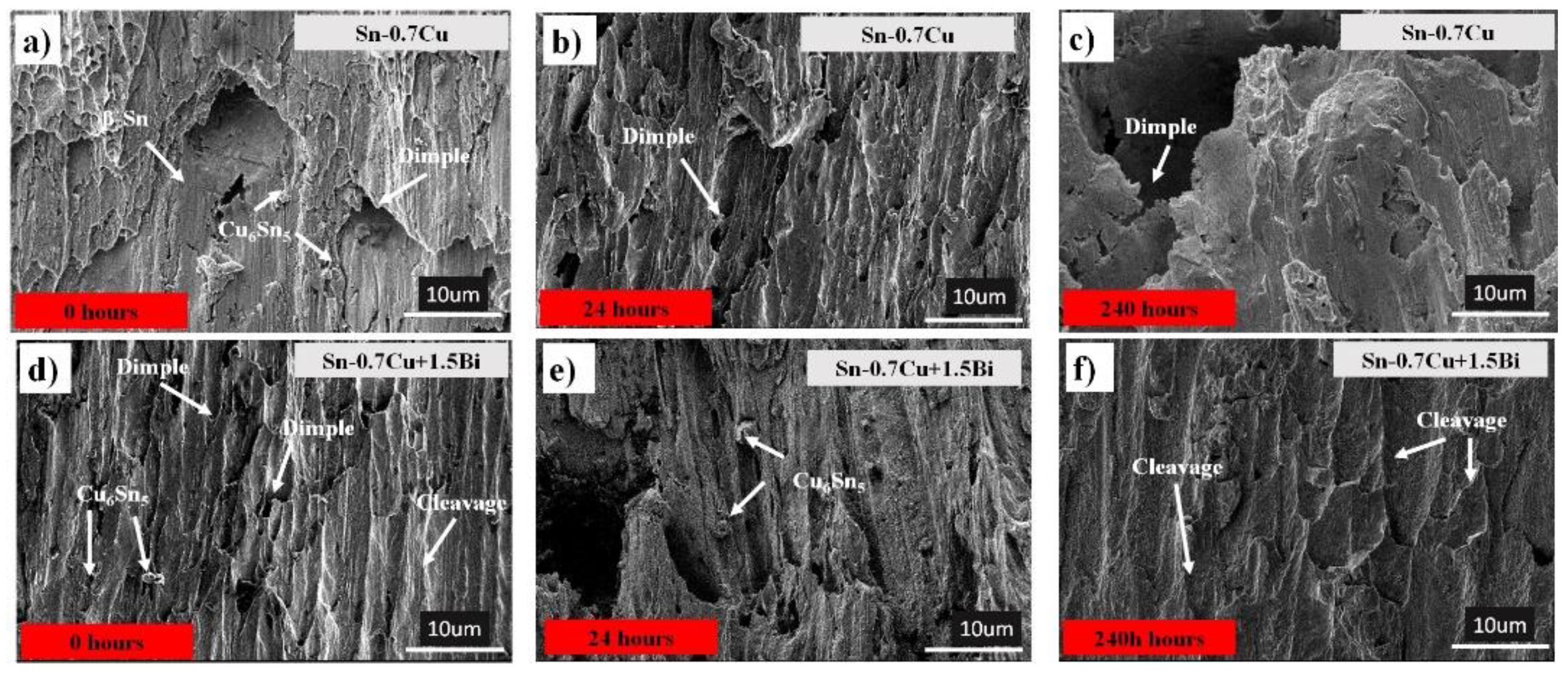
3.4. Fracture Morphology
4. Conclusions
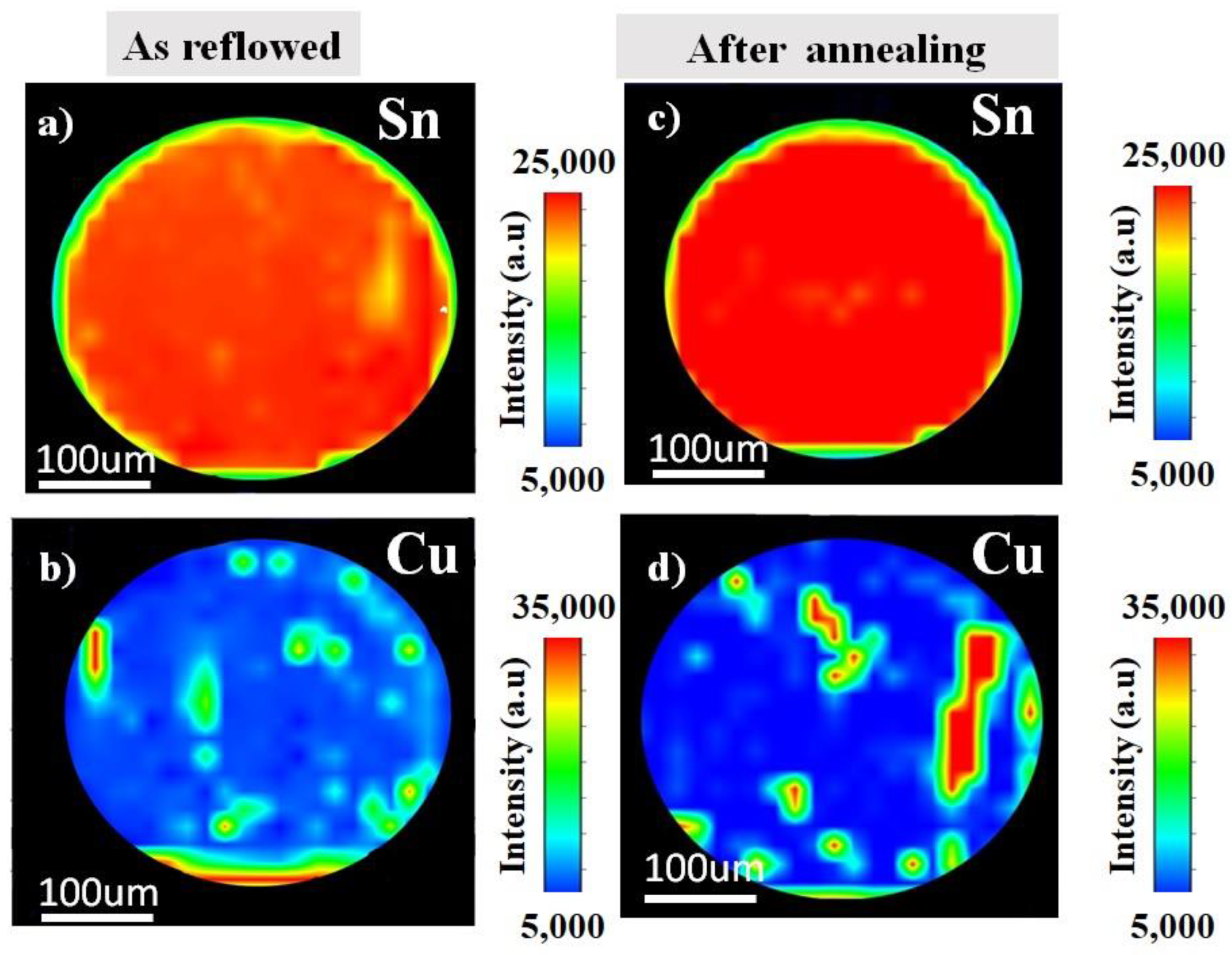
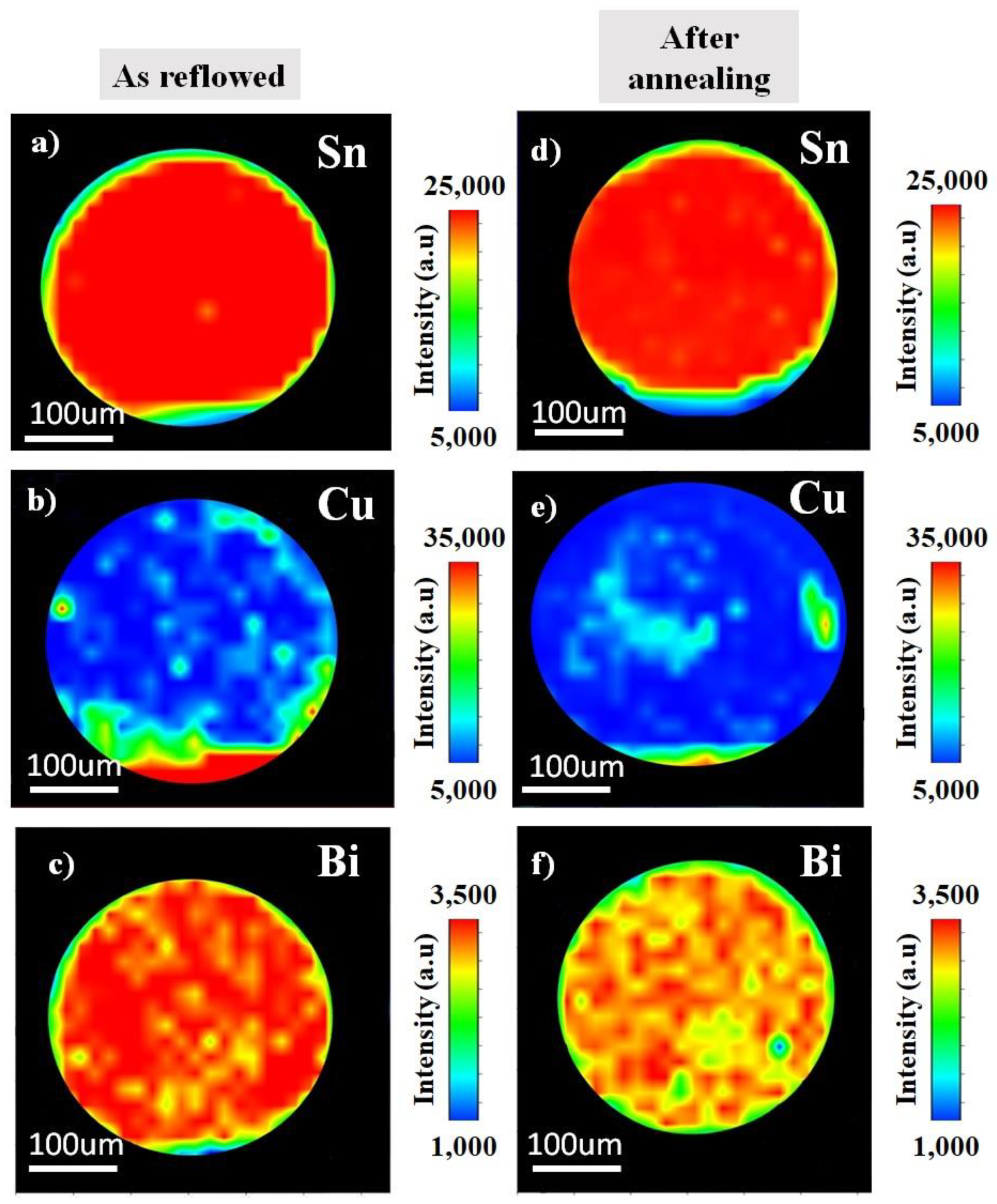
- The 1.5 wt.% Bi addition did not lead to a significant change in the primary Cu6Sn5, as was observed in the bulk solder Sn-0.7Cu. The µ-XRF analysis shows the lower Cu concentration level of Cu6Sn5 primary intermetallic with the addition of Bi after the annealing process. It can also be seen that the Bi element is well dispersed in the β-Sn region.
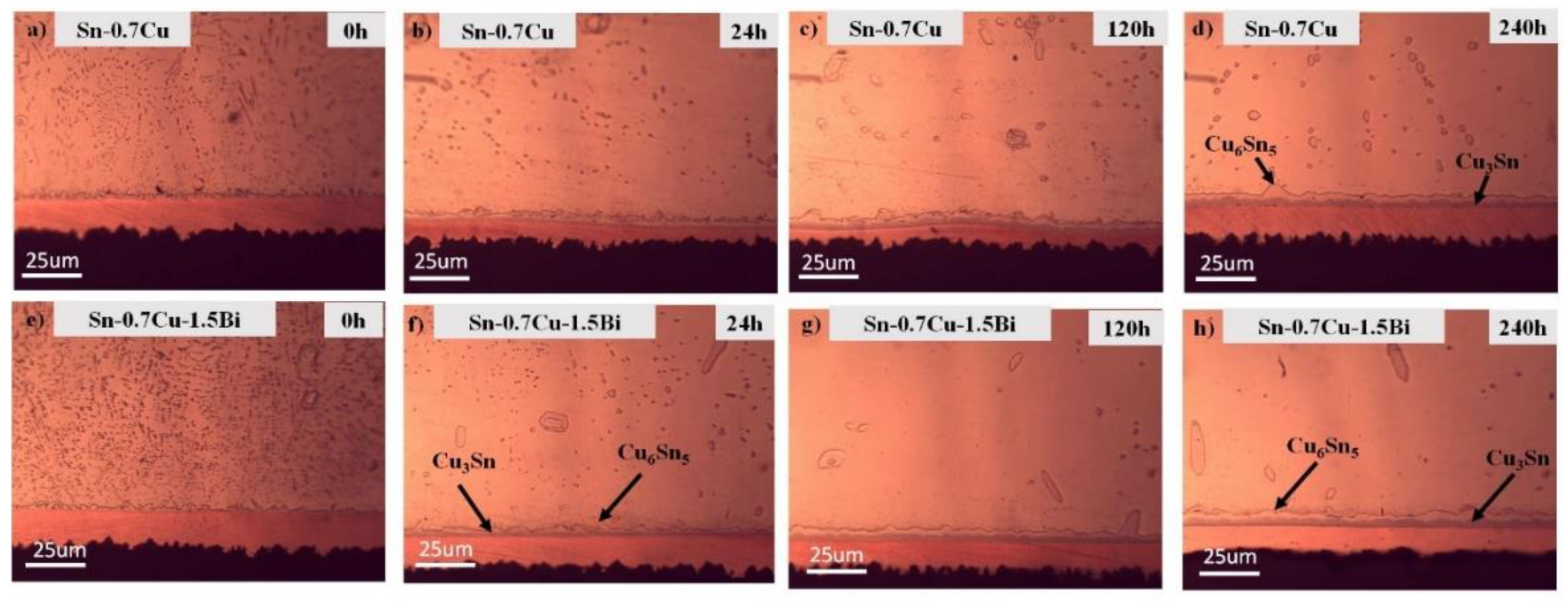
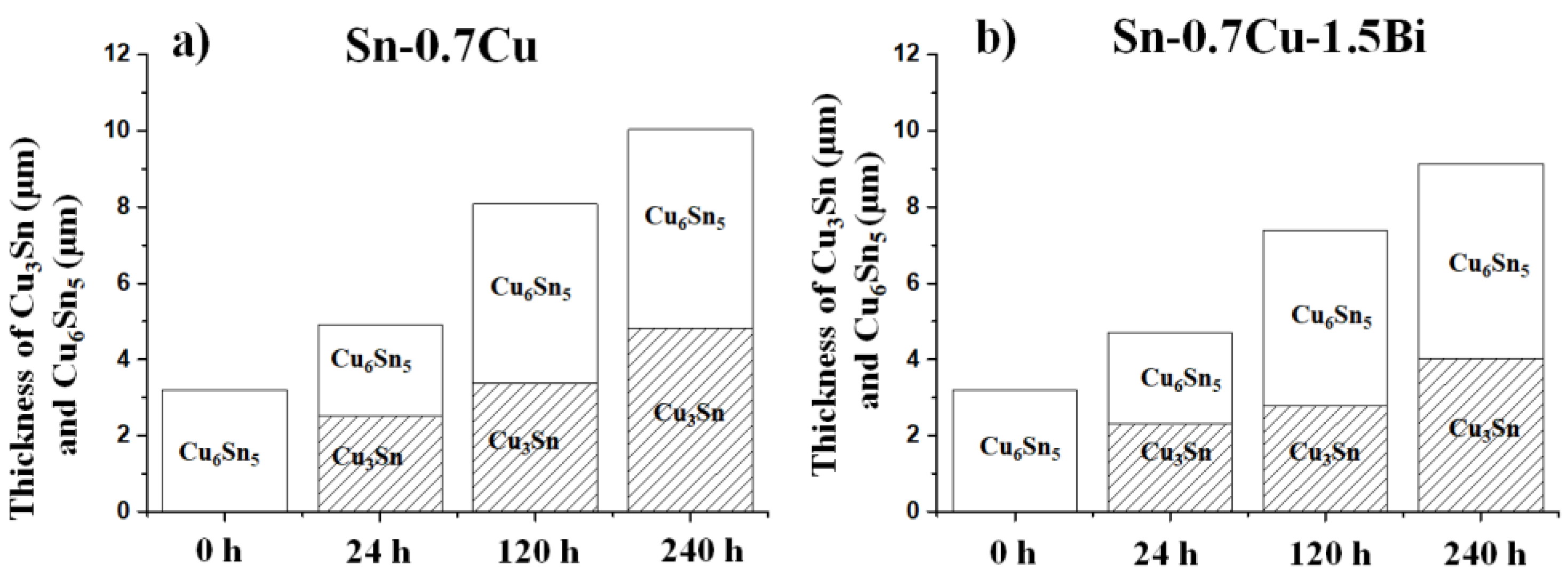
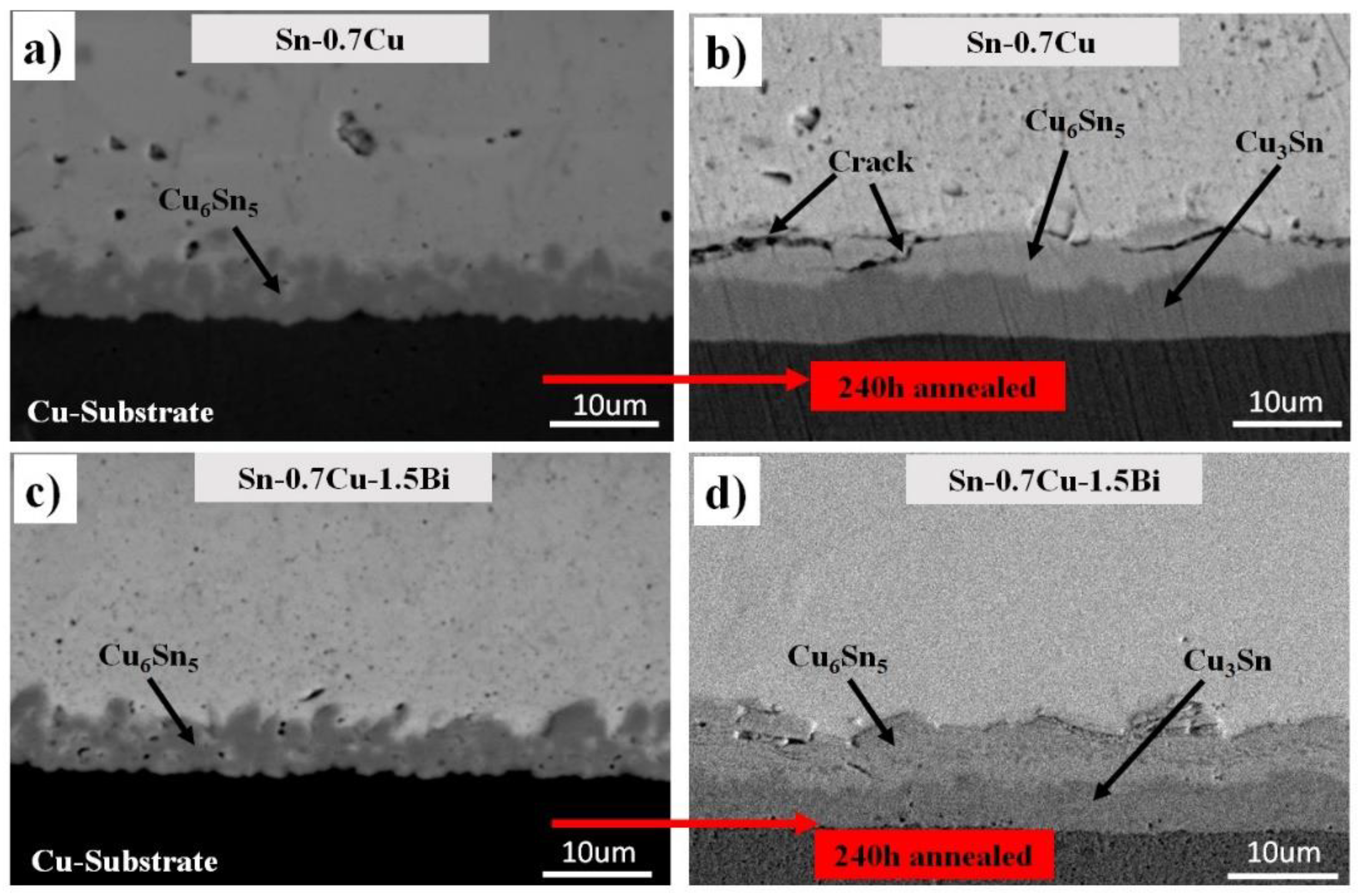
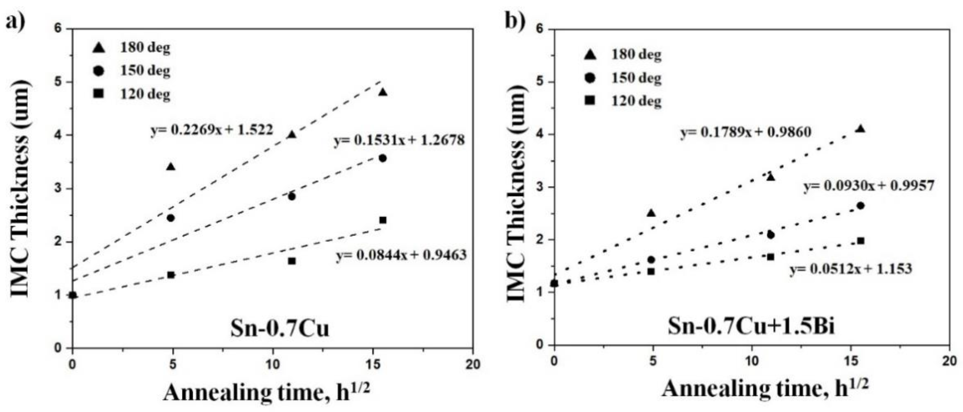
- The growth of interfacial IMC thickness (Cu6Sn5 + Cu3Sn) increases with the annealing process at a rate of 0.042 µm/h for Sn-0.7Cu and 0.037 µm/h for Sn-0.7Cu-1.5Bi. The shape shifted from the scallop shape to the planar shape after the annealing process with a small microcrack form. Bi also inhibited the growth of Cu3Sn interfacial intermetallic compound after the annealing process.
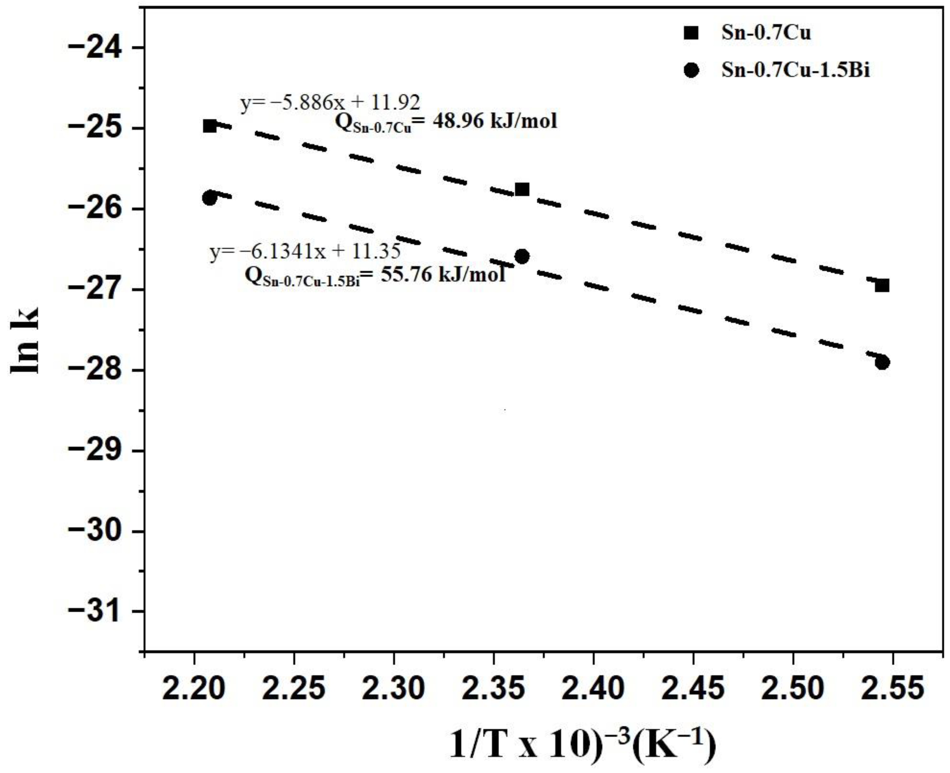
- The activation energy for the formation of intermetallic layers of Sn-0.7Cu was set to 48.96 kJ mol−1, and the activation energy of the Sn-0.7Cu-1.5Bi system was measured at 55.76 kJ mol−1. It is obvious that the intermetallic compound thickness of the Sn-0.7Cu-1.5Bi system is difficult to grow when matched to the Sn-0.7Cu system due to the high activation energy.
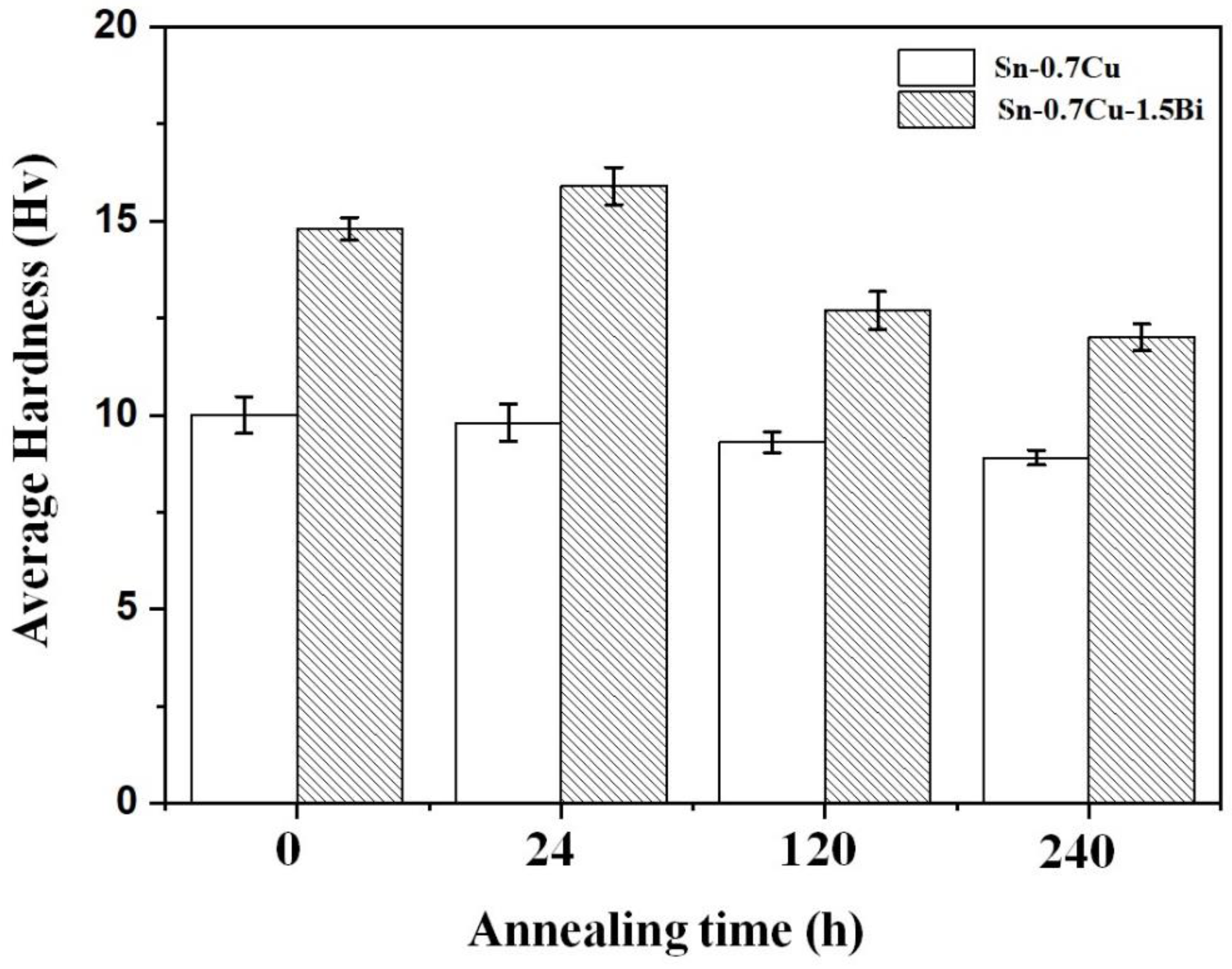
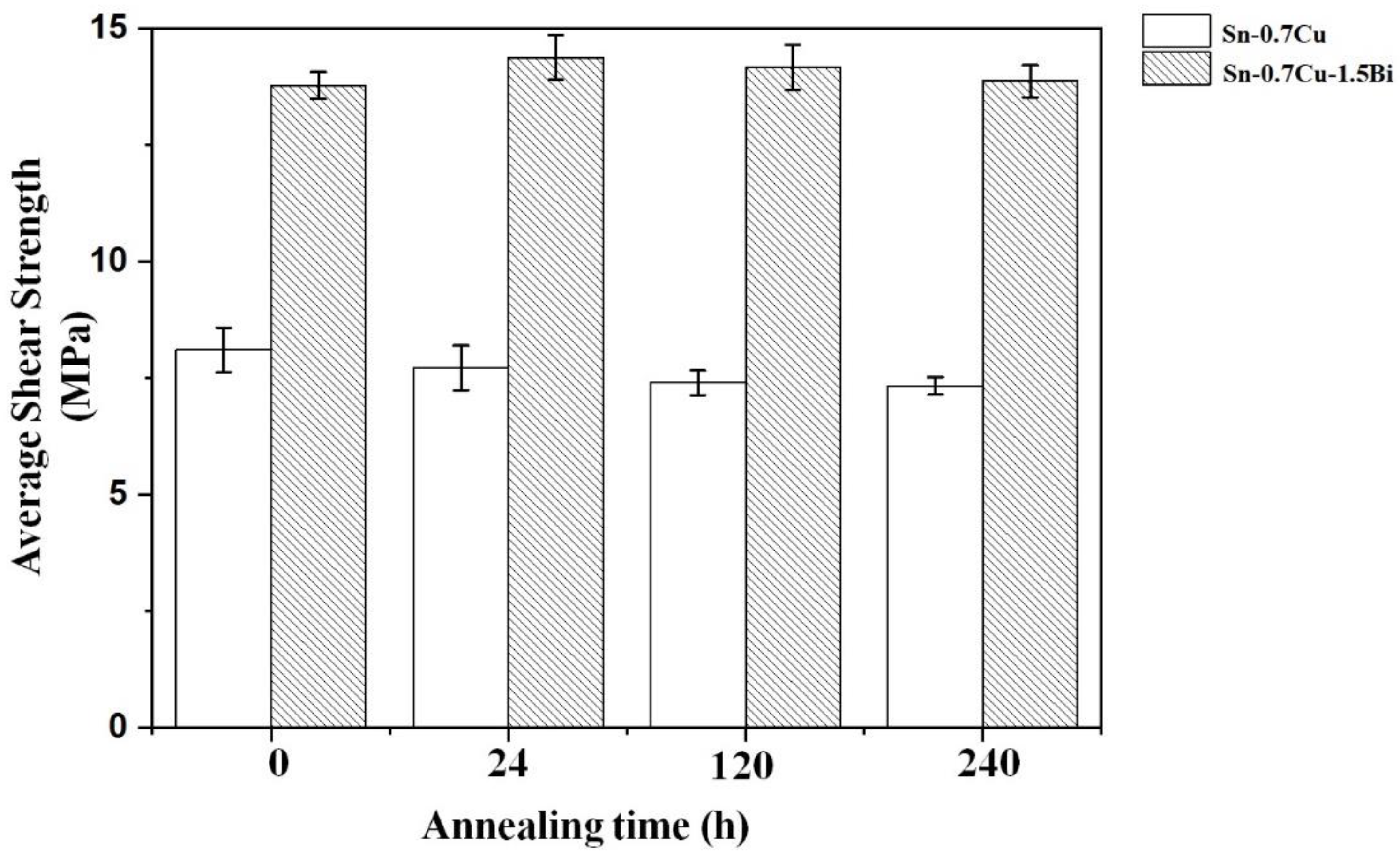
- Compared to Sn-0.7Cu, adding Bi improves hardness by 40.3% and shear strength by 37.1%. After 24 h of annealing, the shear strength of Sn-0.7Cu-1.5Bi was increased. This is due to the fact that with the addition of Bi, it can be that the dissolution of the Bi element in the matrix improved the shear performance of the solder joint. However, a longer annealing time could reduce the shear strength. The fracture of the annealing sample shows a mixture of brittle fractures in the area near the solder/intermetallic interface due to a thicker intermetallic compound layer during the annealing process.
Author Contributions
Funding
Institutional Review Board Statement
Informed Consent Statement
Data Availability Statement
Conflicts of Interest
References
- Ramli, M.I.I.; Salleh, M.A.A.M.; Yasuda, H.; Chaiprapa, J.; Nogita, K. The effect of Bi on the Microstructure, Electrical, Wettability and Mechanical Properties of Sn-0.7Cu-0.05Ni alloys for High Strength Soldering. Mater. Des. 2019, 186, 108281. [Google Scholar] [CrossRef]
- Teoh, A.; Salleh, M.M.; Halin, D.; Foo, K.; Razak, N.A.; Yasuda, H.; Nogita, K. Microstructure, thermal behavior and joint strength of Sn-0.7 Cu-1.5 B[1]i/electroless nickel immersion gold (ENIG). J. Mater. Res. Technol. 2021, 12, 1700–1714. [Google Scholar] [CrossRef]
- Bogno, A.-A.; Spinelli, J.E.; Afonso, C.R.M.; Henein, H. Microstructural and mechanical properties analysis of extruded Sn–0.7 Cu solder alloy. J. Mater. Res. Technol. 2015, 4, 84–92. [Google Scholar] [CrossRef] [Green Version]
- Rizvi, M.J.; Chan, Y.C.; Bailey, C.; Lu, H.; Islam, M.N. Effect of adding 1 wt% Bi into the Sn-2.8Ag-0.5Cu solder alloy on the intermetallic formations with Cu-substrate during soldering and isothermal aging. J. Alloy. Compd. 2006, 407, 208–214. [Google Scholar] [CrossRef]
- Zhao, J.; Cheng, C.-Q.; Qi, L.; Chi, C.-Y. Kinetics of intermetallic compound layers and shear strength in Bi-bearing SnAgCu/Cu soldering couples. J. Alloy. Compd. 2009, 473, 382–388. [Google Scholar] [CrossRef]
- Zhao, J.; Qi, L.; Wang, X.M.; Wang, L. Influence of Bi on microstructures evolution and mechanical properties in Sn-Ag-Cu lead-free solder. J. Alloy. Compd. 2004, 375, 196–201. [Google Scholar] [CrossRef]
- Wang, K.K.; Gan, D.; Hsieh, K.C. Orientation relationships, interfaces, and microstructure of η-Cu6Sn5 formed in the early-stage reaction between Cu and molten Sn. Thin Solid Film. 2010, 519, 1380–1386. [Google Scholar] [CrossRef]
- Sayyadi, R.; Khodabakhshi, F.; Javid, N.S.; Khatibi, G. Influence of graphene content and nickel decoration on the microstructural and mechanical characteristics of the Cu/Sn–Ag–Cu/Cu soldered joint. J. Mater. Res. Technol. 2020, 9, 8953–8970. [Google Scholar] [CrossRef]
- Shen, J.; Zhao, M.; He, P.; Pu, Y. Growth behaviors of intermetallic compounds at Sn-3Ag-0.5Cu/Cu interface during isothermal and non-isothermal aging. J. Alloy. Compd. 2013, 574, 451–458. [Google Scholar] [CrossRef]
- Zhang, L.; Xue, S.B.; Zeng, G.; Gao, L.L.; Ye, H. Interface reaction between SnAgCu/SnAgCuCe solders and Cu substrate subjected to thermal cycling and isothermal aging. J. Alloy. Compd. 2012, 510, 38–45. [Google Scholar] [CrossRef]
- Nergis, D.D.B.; Vizureanu, P.; Ardelean, I.; Sandu, A.V.; Corbu, O.; Matei, E. Revealing the Influence of Microparticles on Geopolymers’ Synthesis and Porosity. Materials 2020, 13, 3211. [Google Scholar] [CrossRef] [PubMed]
- Shen, J.; Cao, Z.; Zhai, D.; Zhao, M.; He, P. Effect of isothermal aging and low density current on intermetallic compound growth rate in lead-free solder interface. Microelectron. Reliab. 2014, 54, 252–258. [Google Scholar] [CrossRef]
- Deng, X.; Sidhu, R.S.; Johnson, P.; Chawla, N. Influence of reflow and thermal aging on the shear strength and fracture behavior of Sn-3.5 Ag solder/Cu joints. Metall. Mater. Trans. A 2005, 36, 55–64. [Google Scholar] [CrossRef]
- Aamir, M.; Muhammad, R.; Ahmed, N.; Sadiq, M.; Waqas, M. Izhar, Mechanical Properties of Lead Free Solder Alloy for Green Electronics under High Strain Rate and Thermal Aging. J. Eng. Appl. Sci. 2017. [Google Scholar] [CrossRef]
- Mahdavifarda, M.H.; Sabria, M.F.M.; Saidb, S.M.; Rozalia, S. High stability and aging resistance Sn-1Ag-0.5Cu solder alloy by Fe and Bi minor alloying. Microelectron. Eng. 2019, 208, 29–38. [Google Scholar] [CrossRef]
- Tateyama, H.U.K.; Yamaoka, Y.; Takahashi, K.; Yamada, H.; Saito, M. Effects of Bi Content on Mechanical Properties and Bump Interconnection Reliability of Sn-Ag Solder Alloys. Int. J. Microcircuits Electron. Packag. 2000, 23, 1063–1674. [Google Scholar]
- Delhaise, A.M.; Chen, Z.; Perovic, D.D. Solid-State Diffusion of Bi in Sn: Effects of b-Sn Grain Orientation. J. Electron. Mater. 2019, 48, 32–43. [Google Scholar] [CrossRef]
- Ahmed, S.; Basit, M.; Suhling, J.C.; Lall, P. Effects of aging on SAC-Bi solder materials. In Proceedings of the 2016 15th IEEE Intersociety Conference on Thermal and Thermomechanical Phenomena in Electronic Systems (ITherm), Las Vegas, NV, USA, 31 May–3 June 2016; IEEE: Piscataway, NJ, USA, 2016; pp. 746–754. [Google Scholar]
- Mohd Said, R.; Mohd Salleh, M.A.A.; Saud, N.; Ramli, M.I.I.; Yasuda, H.; Nogita, K. Microstructure and growth kinetic study in Sn–Cu transient liquid phase sintering solder paste. J. Mater. Sci-Mater. El. 2020, 31, 11077–11094. [Google Scholar] [CrossRef]
- Muhd Amli, S.F.N.; Mohd Salleh, M.A.A.; Ramli, M.I.I.; Yasuda, H.; Chaiprapa, J.; Somidin, F.; Shayfull, Z.; Nogita, K. Origin of Primary Cu6Sn5 in Hypoeutectic Solder Alloys and a Method of Suppression to Improve Mechanical Properties. J. Electron. Mater. 2021, 50, 710–722. [Google Scholar] [CrossRef]

Publisher’s Note: MDPI stays neutral with regard to jurisdictional claims in published maps and institutional affiliations. |
© 2021 by the authors. Licensee MDPI, Basel, Switzerland. This article is an open access article distributed under the terms and conditions of the Creative Commons Attribution (CC BY) license (https://creativecommons.org/licenses/by/4.0/).
Share and Cite
Ramli, M.I.I.; Salleh, M.A.A.M.; Sandu, A.V.; Amli, S.F.M.; Said, R.M.; Saud, N.; Abdullah, M.M.A.B.; Vizureanu, P.; Rylski, A.; Chaiprapa, J.; et al. Influence of 1.5 wt.% Bi on the Microstructure, Hardness, and Shear Strength of Sn-0.7Cu Solder Joints after Isothermal Annealing. Materials 2021, 14, 5134. https://doi.org/10.3390/ma14185134
Ramli MII, Salleh MAAM, Sandu AV, Amli SFM, Said RM, Saud N, Abdullah MMAB, Vizureanu P, Rylski A, Chaiprapa J, et al. Influence of 1.5 wt.% Bi on the Microstructure, Hardness, and Shear Strength of Sn-0.7Cu Solder Joints after Isothermal Annealing. Materials. 2021; 14(18):5134. https://doi.org/10.3390/ma14185134
Chicago/Turabian StyleRamli, Mohd Izrul Izwan, Mohd Arif Anuar Mohd Salleh, Andrei Victor Sandu, Siti Farahnabilah Muhd Amli, Rita Mohd Said, Norainiza Saud, Mohd Mustafa Al Bakri Abdullah, Petrica Vizureanu, Adam Rylski, Jitrin Chaiprapa, and et al. 2021. "Influence of 1.5 wt.% Bi on the Microstructure, Hardness, and Shear Strength of Sn-0.7Cu Solder Joints after Isothermal Annealing" Materials 14, no. 18: 5134. https://doi.org/10.3390/ma14185134
APA StyleRamli, M. I. I., Salleh, M. A. A. M., Sandu, A. V., Amli, S. F. M., Said, R. M., Saud, N., Abdullah, M. M. A. B., Vizureanu, P., Rylski, A., Chaiprapa, J., & Nabialek, M. (2021). Influence of 1.5 wt.% Bi on the Microstructure, Hardness, and Shear Strength of Sn-0.7Cu Solder Joints after Isothermal Annealing. Materials, 14(18), 5134. https://doi.org/10.3390/ma14185134