Article

Surface Modification of Nanoporous Anodic Alumina during Self-Catalytic Atomic Layer Deposition of Silicon Dioxide from (3-Aminopropyl)Triethoxysilane

by
Ana Silvia González
1,*,
Víctor Vega
2,
Ana Laura Cuevas
3,
María del Valle Martínez de Yuso
4,
Víctor M. Prida
1 and
Juana Benavente
5
1
Departamento de Física, Facultad de Ciencias, Universidad de Oviedo, E-33007 Oviedo, Spain
2
Laboratorio de Membranas Nanoporosas, Servicios Científico-Técnicos, Universidad de Oviedo, E-33006 Oviedo, Spain
3
Unidad de Nanotecnología, SCBI Centro, Universidad de Málaga, E-29071 Málaga, Spain
4
Servicios Centrales de Investigación, Universidad de Málaga, E-29071 Málaga, Spain
5
Departmento de Física Aplicada I, Facultad de Ciencias, Universidad de Málaga, E-29071 Málaga, Spain
*
Author to whom correspondence should be addressed.
Materials 2021, 14(17), 5052; https://doi.org/10.3390/ma14175052
Submission received: 23 July 2021 / Revised: 26 August 2021 / Accepted: 30 August 2021 / Published: 3 September 2021
(This article belongs to the Special Issue Advances in Electrochemistry of Nanomaterials)

Abstract

:
Changes associated to atomic layer deposition (ALD) of SiO2 from 3-aminopropyl triethoxysilane (APTES) and O3, on a nanoporous alumina structure, obtained by two-step electrochemical anodization in oxalic acid electrolyte (Ox sample) are analysed. A reduction of 16% in pore size for the Ox sample, used as support, was determined by SEM analysis after its coverage by a SiO2 layer (Ox+SiO2 sample), independently of APTES or O3 modification (Ox+SiO2/APTES and Ox+SiO2/APTES/O3 samples). Chemical surface modification was determined by X-ray photoelectron spectroscopy (XPS) technique during the different stages of the ALD process, and differences induced at the surface level on the Ox nanoporous alumina substrate seem to affect interfacial effects of both samples when they are in contact with an electrolyte solution according to electrochemical impedance spectroscopy (EIS) measurements, or their refraction index as determined by spectroscopic ellipsometry (SE) technique. However, no substantial differences in properties related to the nanoporous structure of anodic alumina (photoluminescent (PL) character or geometrical parameters) were observed between Ox+SiO2/APTES and Ox+SiO2/APTES/O3 samples.

1. Introduction

Atomic Layer Deposition (ALD), formerly known as atomic layer epitaxy, is nowadays a well-stablished technique allowing for the deposition of smooth and pinhole-free thin films of several materials, namely oxides, nitrides, and sulfides, among others [1,2,3]. Furthermore, ALD enables the deposition of conformal coatings even in three-dimensional, high aspect ratio nanostructured substrates, while keeping an accurate control on the thickness and stoichiometry of the deposits [4]. These features arise from the self-limited nature of the ALD technique, in which reaction kinetics are controlled by surface chemistry, rather than by mass transport phenomena [5]. From all the above reasons, ALD constitutes an outstanding deposition technique, being specifically suitable for surface coating of nanoporous structures, such as nanoporous anodic alumina or polymeric track-etched membranes [4,6,7,8]. Depending on the material of choice for the ALD deposition, different features of nanoporous membranes can be tuned or improved. In fact, nanoporous alumina structures (NPASs) or membranes (NPAMs) obtained by electrochemical anodization of aluminium (two step anodization method [9,10]) consisting in a parallel array of cylindrical pores with narrow pore radius distribution and without tortuosity, whose geometrical parameters (pore size, interpore distance and pore length) can be selected depending on the electrochemical anodization conditions have demonstrated to be adequate supports for ALD deposition of one or two layers of different ceramic oxides, thus enabling to modify their pore-size/porosity and physicochemical characteristics (surface chemistry, selectivity, electrical and diffusive properties) as well as optical characteristics (refraction index, light transmission,…) [7,8,11,12]. Lately, NPASs have been considered as very good candidates to develop chemical/biological sensors due to their biocompatibility (which can be improved by a given coating layer) and high aspect ratio, which favours the enhancement of optical signals by pore-walls modification with specific molecules [13,14].
On the other hand, silicon dioxide is a material of particular interest for membrane modification due to its dielectric nature, high chemical and thermal stability. In this context, silica-alumina composite membranes synthesized through chemical vapor deposition (CVD) of tetraethylorthosilicate (TEOS) and aluminium tri-sec-butoxide precursor have been proposed for application in membrane reactors due to their high gas permeation and selectivity [15] The ALD deposition of conformal SiO2 films from a wide variety of silane precursors, including tetraethoxysilane, tris[dimethylamino]silane, bis[diethylamino]silane, (N,N-dimethylamino)trimethylsilane, vinyltrimethoxysilane, trivinylmethoxysilane, tetrakis(dimethylamino)silane, tris(dimethylamino)silane, tetrakis(ethylamino)silane, aminodisilane and 3-aminopropyltriethoxysilane (APTES) has been explored in the literature, [16,17,18,19,20,21,22]. This work focuses on the thermal ALD deposition process based on the self-catalytic reaction between 3-aminopropyltriethoxysilane, water, and ozone as precursors. The main advantages of this SiO2 deposition approach, based on APTES precursor, lies in the fact that it shows a high degree of thickness control and remarkably good surface coverage even into nanoscale pores, which can be achieved at low growth temperatures of 120–200 °C [22]. Also, APTES precursor is noncorrosive, liquid at room temperature, with sufficient vapor pressure under moderate heating, and commercially available at low cost [23]. Consequently, ALD of SiO2 offers exceptional deposition conformality with high aspect ratio even for nanoporous structures like alumina templates [23,24]. In addition, application of APTES modified polymeric membranes and APTES functionalized alumina monoliths for the immobilization of molecules (biotin, rabbit IgG,...) or effective purification of immunoglobulins, respectively, have already been reported [25,26,27,28], opening the field of application of APTES-modified NPAMs.
Another important aspect is that the ALD of SiO2 is a three-step reaction sequence based on the subsequent exposure of substrates to APTES, water, and ozone (O3), as it can be observed in Figure 1, where it is possible to see that in the first step APTES is chemisorbed onto the surface of the substrate material (Figure 1a), after this, during the H2O cycle, the aminopropyl groups existing in APTES catalyze the hydrolysis of ethoxy ligands, leaving the surface terminated with OH groups (Figure 1b). In addition, during the O3 cycle, occurs the combustion of the remaining aminopropyl ligands, enabling the production of combustion gases such as CO, CO2, H2O, and NOx. As it was already indicated [29] among these by-products, CO reacts with surface OH groups to form monodentate formates and SiH on the surface (Figure 1c). Finally, the monodentate formates with SiH groups, along with the OH groups, produced during H2O exposure, serve as the reactive sites for APTES chemisorption, thus completing the entire ALD cycle [22,23,29]. As a result, surface functional groups change during the different steps that take place during a SiO2 ALD deposition cycle, ranging from etoxy, amino and hydroxide groups. This causes that the same material may have slightly different surface groups, which in turn may affect its physicochemical and/or transport properties.
In this work, we analyzed the chemical change caused in a nanoporous alumina structure after being modified with a SiO2 layer by ALD technique, which exhibits two different surface terminations (with amino or monodentate formates groups), as indicated in Figure 1a,c, as well as the changes that such terminations provokes in different parameters of interest for sample applications. These changes have been studied by means of several characterization techniques such as scanning electron microscopy (SEM), X-ray photoelectron spectroscopy (XPS), electrochemical impedance spectroscopy (EIS) and diverse optical techniques (photoluminescence, transmittance and spectroscopic ellipsometry measurements), in order to have a complete characterization of the modified samples.

2. Materials and Methods

2.1. Materials

The nanoporous alumina structure (NPAS) used as support was synthesized by the well-stablished two step anodization method [9,10]. In brief, high purity (99.999%) Al foils (SMP, Barcelona, Spain) with a thickness of 0.5 mm were cut into discs of 25 mm in diameter, thoroughly cleaned by sonication in isopropyl and ethyl alcohols and electropolished in a mixture of perchloric acid in ethanol (1:3 vol.) at 5 °C under an anodic voltage of 20 V, applied between the Al foils and a platinum counter-electrode. Afterwards, the aluminum substrates were rinsed in ultrapure water (18.2 MΩ·cm) and submitted to a first anodization process in a mechanically stirred 0.3 M oxalic acid electrolyte, kept at 0–3 °C by an external recirculating bath. An anodization voltage of 40 V measured versus a Pt counter-electrode was applied by a computer controlled DC power supply (Keithley 2400 sourcemeter, Keithley Instruments, Inc., Cleveland, OH, USA) for 24 h, in order to promote the growth of a self-ordered nanoporous alumina structure [9,10].
The nanoporous oxide layer grown during the first anodization step was selectively etched in an aqueous mixture of CrO3 and H3PO4, at room temperature for 48 h, thus leading to a nanostructured Al surface which retains a regular arrangement of dimples left by the pore bottoms during the first anodization step. A second anodization step, performed under the same electrochemical conditions as the first one is then carried out, the duration of which was adjusted to 33 h in order to obtain a nanoporous alumina sample with around of 60 µm in thickness, according with the oxide growth rate of approximately 1.8 µm/h which has been experimentally measured. The remaining Al substrate was selectively removed by exposing the backside of the samples to CuCl2 and HCl aqueous solution, whereas the alumina barrier layer occluding the pores bottom was dissolved by wet chemical etching in 5% wt. orthophosphoric acid at room temperature for 3 h (sample Ox), also resulting in a noticeable increase in pore size from the starting average pore diameter of 35 nm to around 48 nm.
ALD SiO2 coating was carried out in a thermal ALD reactor (Savannah 100, Cambridge Nanotech, Waltham, MA, USA), operated in exposure mode. The precursors employed for SiO2 deposition were APTES (100 °C), water (60 °C) and ozone (20 °C) for SiO2, whereas the reaction chamber was kept at 180 °C throughout the ALD processes. A constant flow of 50 sccm of high purity argon gas was employed as both, purge and carrier gas. Additional details of the ALD deposition sequence can be found elsewhere [7,12]. A total of 80 deposition cycles were performed, being the ALD process stopped after an additional APTES pulse (sample Ox+SiO2/APTES) or after an APTES/H2O/O3 pulse sequence (sample Ox+SiO2/APTES/O3).

2.2. SEM Characterization

The morphology of the nanoporous alumina membranes, including top, bottom and cross-sections views, was studied by scanning electron microscopy (SEM) in a JEOL-5600 Scanning Microscope (Akishima, Tokyo, Japan). Prior to SEM observation, the membranes were coated with a thin gold layer deposited by sputtering (Polaron SC7620, Quorum Technologies, Laughton, UK), in order to improve their electrical conductivity. The geometrical parameters (nanopore size and interpore distance) were measured by computer assisted image analysis using ImageJ (v 1.51j8) [30].

2.3. Chemical Surface Characterization

X-ray photoelectron spectroscopy (XPS), a non-destructive surface sensitive technique, was used to determine the quantity and chemical state of elements present in the surface (or near the surface, around 2–8 nm depth) of the studied samples. XPS spectra were obtained with a Physical Electronics Spectrometer VersaProbe II (Physical Electronics, Chigasaki, Japan) using monochromatic Al-Kα radiation (49.1 W, 15 kV and 1486.6 eV) considering a circular area of 200 μm in diameter, using a hemispherical multichannel detector. The residual pressure in the analysis chamber was maintained below 5 × 10⁻⁷ Pa during data acquisition. Spectra were recorded with a constant pass energy value at 29.35 eV, at a take-off angle of 45 °C, and each spectral region was scanned several times to reduce the noise ratio. Binding energies (B.E. accurate ± 0.1 eV) were determined with respect to the position of the adventitious C 1s peak at 285.0 eV. PHI ACCESS ESCA-V8.0 F software package was used for data acquisition and analysis [31].

2.4. Electrochemical Impedance Spectroscopy Measurements

Electrochemical Impedance Spectroscopy (EIS) is an alternating current (a.c.) technique commonly used for electrical characterization of both homogeneous (solid and liquids) or heterogeneous systems commonly used for electrical characterization of both homogeneous (solid and liquid) or heterogeneous systems [32,33]. EIS measurements were carried out in an electrochemical test-cell as that described in previous papers [33,34], which basically consists of two glass compartments filled with an electrolyte solution of the same concentration, separated by two silicone-rings where the sample (or membrane) was sandwiched, and two electrodes, one into each compartment, connected to a Frequency Response Analyzer (FRA, Solartron 1260, Farnborough, UK). Measurements were performed with NaCl solutions in the system: electrode/NaCl solution (C)//sample//NaCl/solution (C)/electrode, for three different concentration values: C = 2 × 10⁻³ M, 6 × 10⁻³ M and 1 × 10⁻² M. 100 different data points for frequency ranging between 1 Hz and 107 Hz, at maximum voltage of 0.01 V, were recorded. ZView 2 data analysis program (Scribner, Southern Pines, NC, USA) was used for electrical parameters determination.
EIS measurements give quantitative/qualitative information related to charge movement/adsorption from experimental data using equivalent circuits as models [33,34,35] and, under certain conditions, the analysis of EIS diagrams allows us the estimation of different membrane system contributions (membrane, electrolyte and membrane/solution interface). The impedance (Z = Zreal + j Zimg) is a complex number, with real (Zreal) and imaginary (Zimg) parts, which can be expressed for homogeneous systems (a unique relaxation process) as functions of electrical resistance (R) and capacitance (C) of the analysed sample:
Zreal = R/[1 + (ωRC)2]
Zimg =−ωR2 C/[1 + (ωRC)2]
where ω = 2πf is the angular frequency. The analysis of the impedance data is usually performed in the complex plane by analysing the Nyquist plot (−Zimg versus Zreal), where a parallel association of a resistance and a capacitance (RC circuit) corresponds to a semi-circle which intercepts the Zreal axis at R (ω→∞) and Ro (ω→0), being R = 0.5(Ro −R) the electrical resistance of the system, while the maximum of the semi-circle occurs at a frequency such that ωRC = 1 [32]. In the case of non-homogeneous systems Nyquist plot exhibits a depressed semicircle (two or more different relaxation times), and an equivalent capacitance is then considered [32].

2.5. Optical Characterizations

Optical characterization was performed by analysing transmittance, photoluminescence (PL) and spectroscopic ellipsometry (SE) curves.
Light transmission spectra were recorded for wavelengths ranging between 250 nm and 2000 nm, with a Varian Cary 5000 spectrophotometer (Agilent Technologies, Santa Clara, CA, USA) provided with an integrating sphere of Spectralon. Measurements were performed covering samples surface with a mask which exhibits an open area of 0.5 cm × 0.5 cm.
Samples photoluminescence (PL) was measured with a Photoluminiscence Microscope from HORIBA Scientific (LabRam PL Microscope, Horiba Jobin Yvon, Kyoto, Japan), using a 325 nm laser as excitation light source with a beam power of 0.28 mW in the range from 325 to 900 nm.
Spectroscopic ellipsometry (SE) measurements were carried out with a spectroscopic ellipsometer (Sopra-Semilab GES-5E, Budapest, Hungary) at an incident angle of 70° and wavelength ranging between 250 nm and 1700 nm, covering a wide range of visible and near infrared (NIR) regions. Measurements were directly performed on the samples without employing any other substrate.

3. Results and Discussion

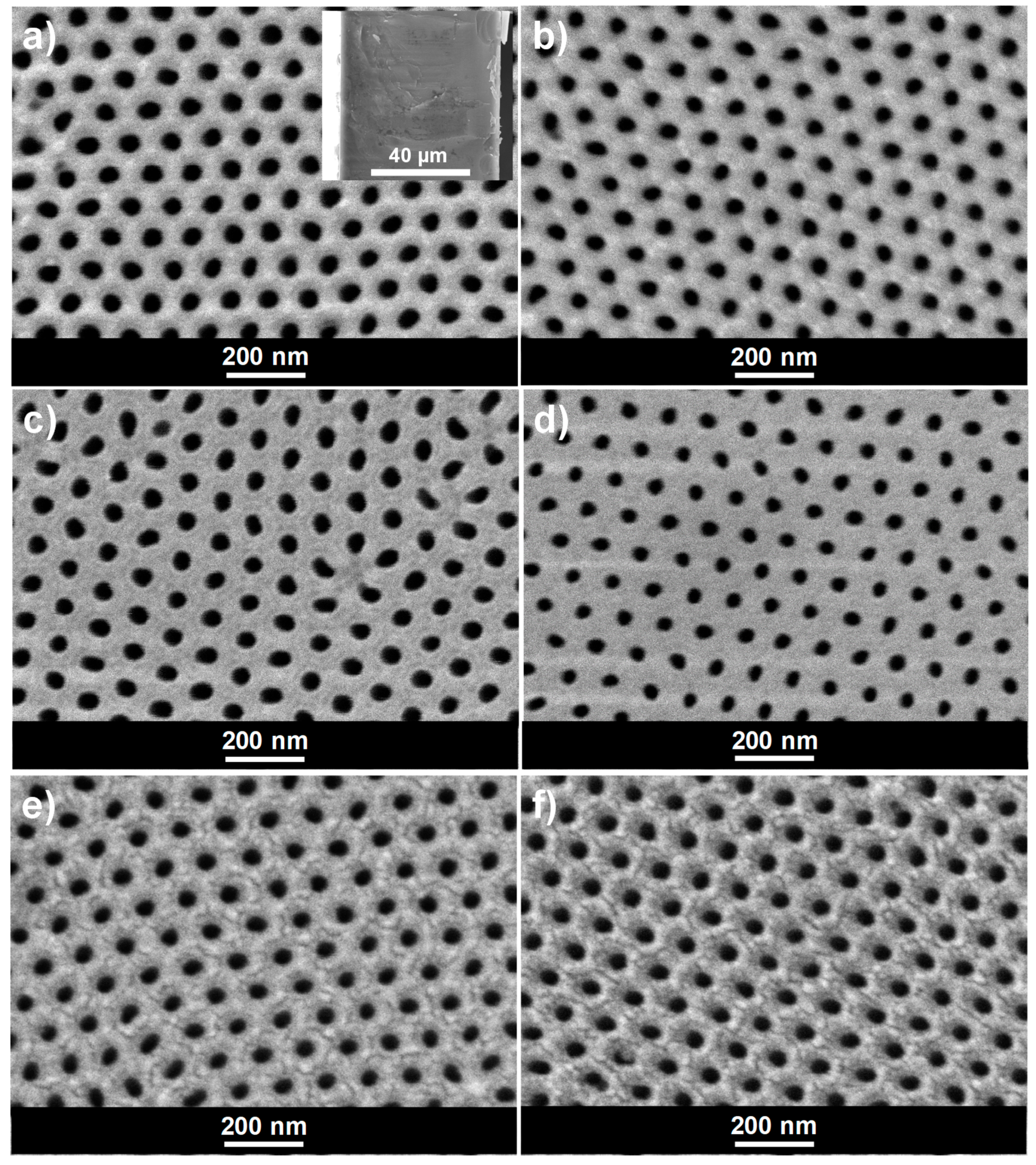
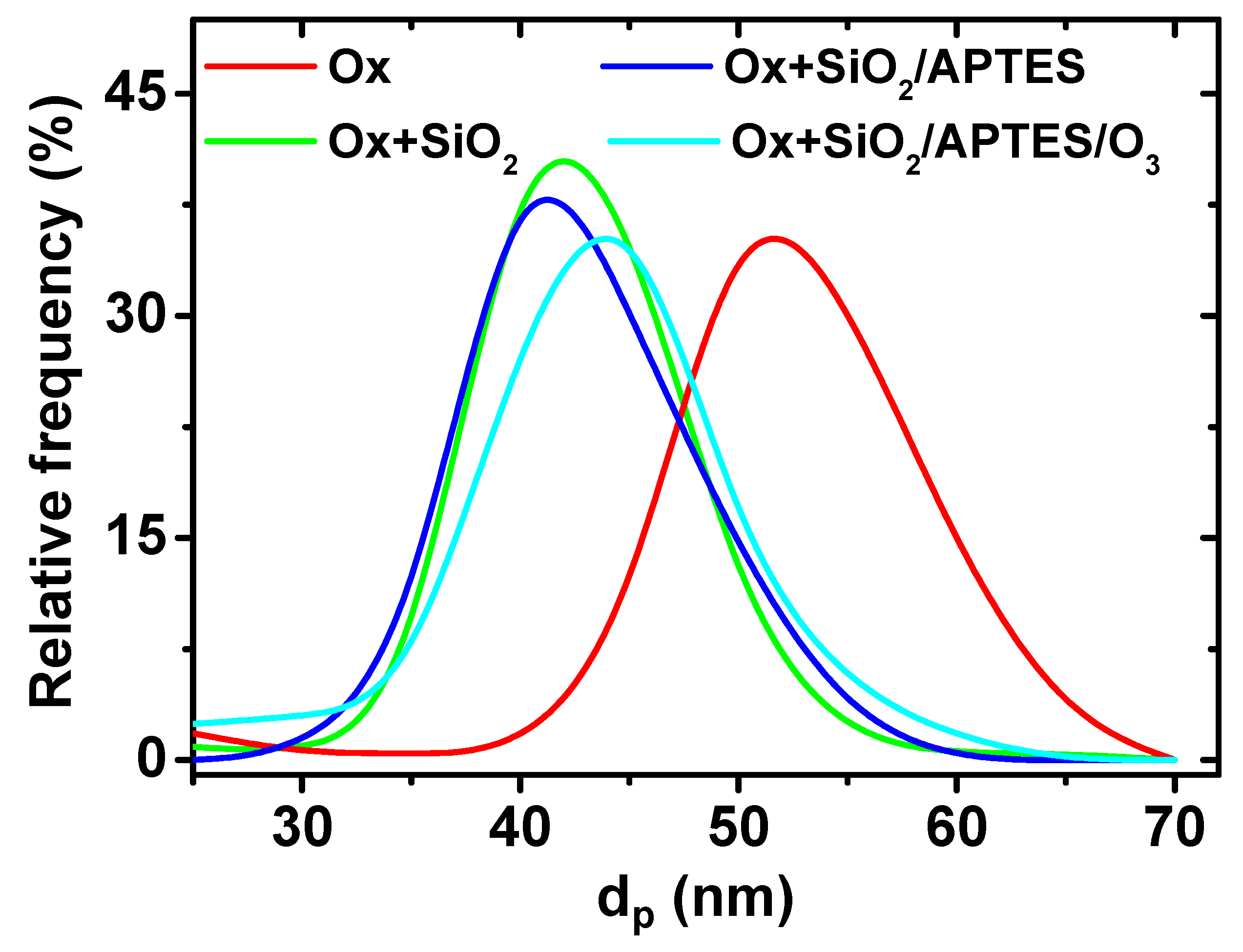
3.1. SEM Characterization

NPAS samples synthesized by the two-step anodization method display a highly ordered pore arrangement with hexagonal symmetry at both, top and bottom sides, as it is evidenced by SEM images shown in Figure 2. Figure 2a,c correspond respectively to the upper and lower surfaces of the as-produced nanoporous alumina sample (Ox), being the corresponding cross-section presented in the inset, whereas images in Figure 2b–f were taken after: Figure 2b,c the ALD deposition of 80 cycles of SiO2 (Ox+SiO2 sample), Figure 2e plus an additional APTES exposure (Ox+SiO2/APTES) and, finally, Figure 2f plus an additional O3 pulse (Ox+SiO2/APTES/O3).
The reduction in the average pore diameter as a result of the SiO2 coating layer becomes evident from the analysis of the pore diameter distribution displayed in Figure 3, by comparison of samples Ox and Ox+SiO2. The average pore diameter was reduced from 48 ± 6 nm down to 40 ± 6 nm as a result of the ALD SiO2 coating, which indicates a thickness of 4 nm for the SiO2 layer. At the same time, SEM images evidence that differences in the average pore diameter among Ox+SiO2, Ox+SiO2/APTES and Ox+SiO2/APTES/O3 samples are practically negligible and, consequently similar pore size/porosity is assumed for these three samples. The interpore distance, which remains unaffected by the ALD coating, takes a value of 105 nm for all the indicated samples. Membranes thickness, evaluated from SEM cross section images (see inset in Figure 2a, takes a value of approximately 60 microns for all the samples.

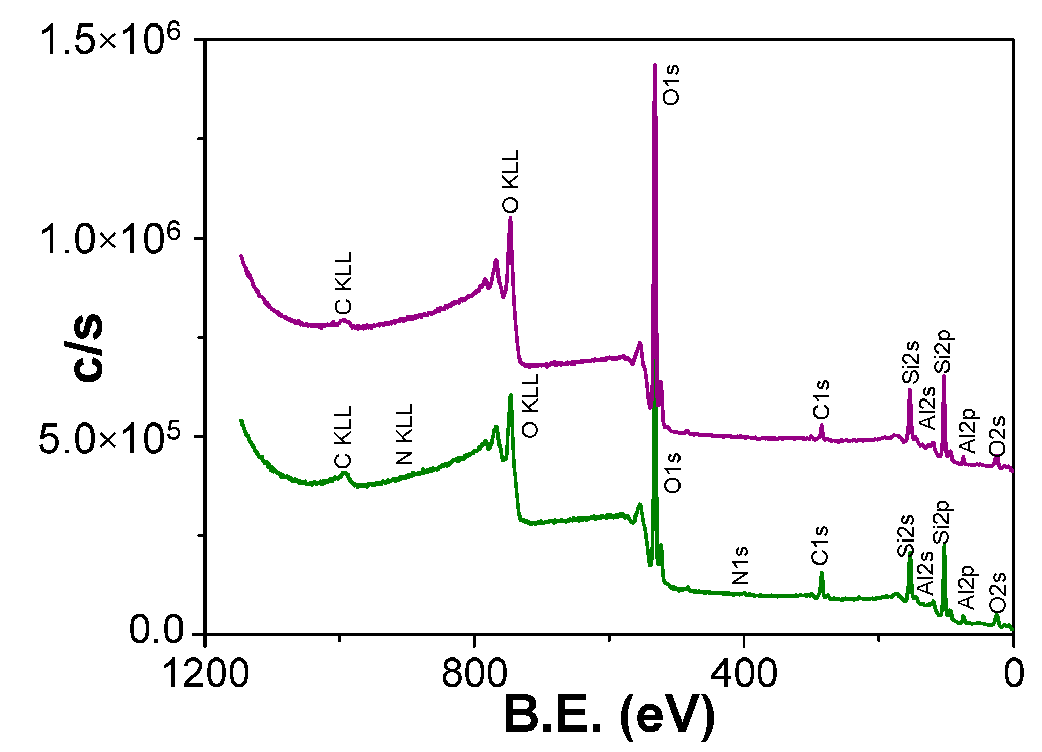
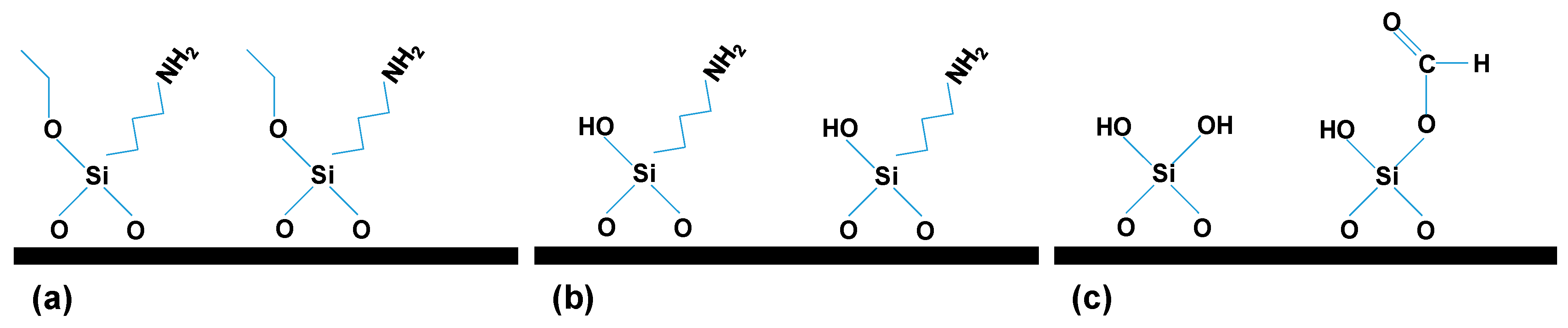
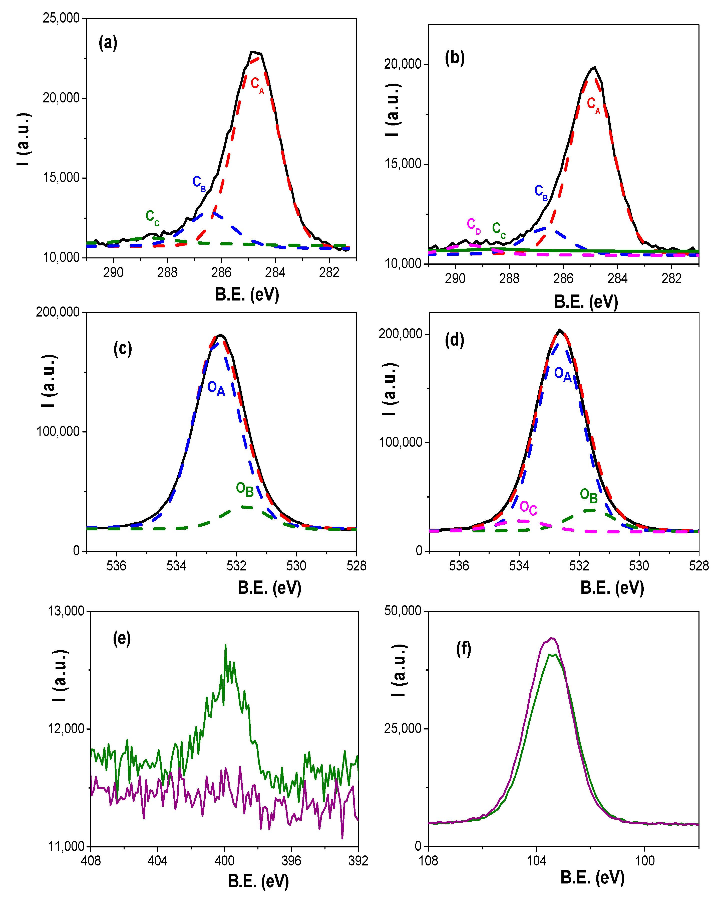
3.2. Chemical Surface Characterization

Chemical surface characterization of Ox+SiO2/APTES and Ox+SiO2/APTES/O3 NPASs was performed by analysing the XPS spectra. Figure 4 shows the survey spectra obtained for each sample, where the characteristic photoemission lines corresponding to C, O, N, Si and Al atoms are labelled
Atomic concentration percentage (A.C. %) of each element was obtained by the corresponding areas, and their values are indicated in Table 1, where the percentages of Si and Al (element associated to the nano-support structure) are also showed; in fact, the relatively low value of this latter element is an indication of adequate coating process. For both samples, carbon core level signal (black solid line in Figure 5a for Ox+SiO2/APTES sample and in Figure 5b for Ox+SiO2/APTES/O3 one) shows a clear peak at 285.0 eV B.E. associated to aliphatic carbon, but other small shoulders at higher binding energy values corresponding to other carbon links are also detected [36], which will be discussed in the next paragraph as well as the slight differences in oxygen core level signal obtained for both samples (black solid line in Figure 5c,d for Ox+SiO2/APTES and Ox+SiO2/APTES/O3, respectively) are also indicative of other contributions different from the high intensity peak at B.E. of 532.6 eV associated to Si–O/SiO2 links [36]. On the other hand, a clear peak at a B.E. of 399.5 eV can be observed in the nitrogen core level spectra (Figure 5e) for the Ox+SiO2/APTES sample but, as expected, the Ox+SiO2/APTES/O3 one does not show any nitrogen contribution, which demonstrates the total elimination of amino groups by O3 treatment; in the case of silicon core level spectra (Figure 5f) both samples show similar curves, with a peak at the B.E. of 103.4 eV.
As it was shown above, the asymmetry of carbon core level spectra is an indication of different carbon links, and three different contributions (represented by dashed lines) are pointed out in Figure 5a for Ox+SiO2/APTES sample but four in Figure 5b for Ox+SiO2/APTES/O3 one: the peak CA (at 285.0 eV B.E.) of higher intensity is associated to C–C or C–H links, while the small shoulders CB (at 286.6 eV B.E.) and CC (at 288.9 eV B.E.) are associated to CO/CN/CSi and C–O bonds, respectively [36]; moreover, another shoulder CD (at 289.4 eV B.E.) associated to the O–C=O bond was also determined in the case of the Ox+SiO2/APTES/O3 sample. The corresponding area percentage and atomic concentration percentage determined for each sample as well as the binding energy values and links are collected in Table 2A.
The O 1s core level spectra for the studied samples shown in Figure 5c,d exhibits a very intense peak at a B.E. of 532.6 eV (OA), associated to Si–O/SiO2 links, but also a small shoulder at 531.6 eV (OB) which corresponds to Al–O bond [36]; however, the Ox+SiO2/APTES/O3 sample also shows another shoulder at a B.E. of 533.9 eV associated to C–O link [36]. Comparison of experimental (black solid line) and fitted (dashed red line) oxygen values are also drawn in Figure 5c,d while area percentage and atomic concentration percentage of the different contributions determined for each sample are also indicated in Table 2B, as well as the corresponding binding energy values and links. In this context, it should be indicated the good concordance existing between the aluminum atomic concentration % directly obtained from Al core level area for Ox+SiO2/APTES and Ox+SiO2/APTES/O3 samples indicated in Table 1 (4.0 and 3.9%), and those determined from oxygen A.C. % for Al–O link shown in Table 2B, taking into account, Al2O3 stoichiometry.

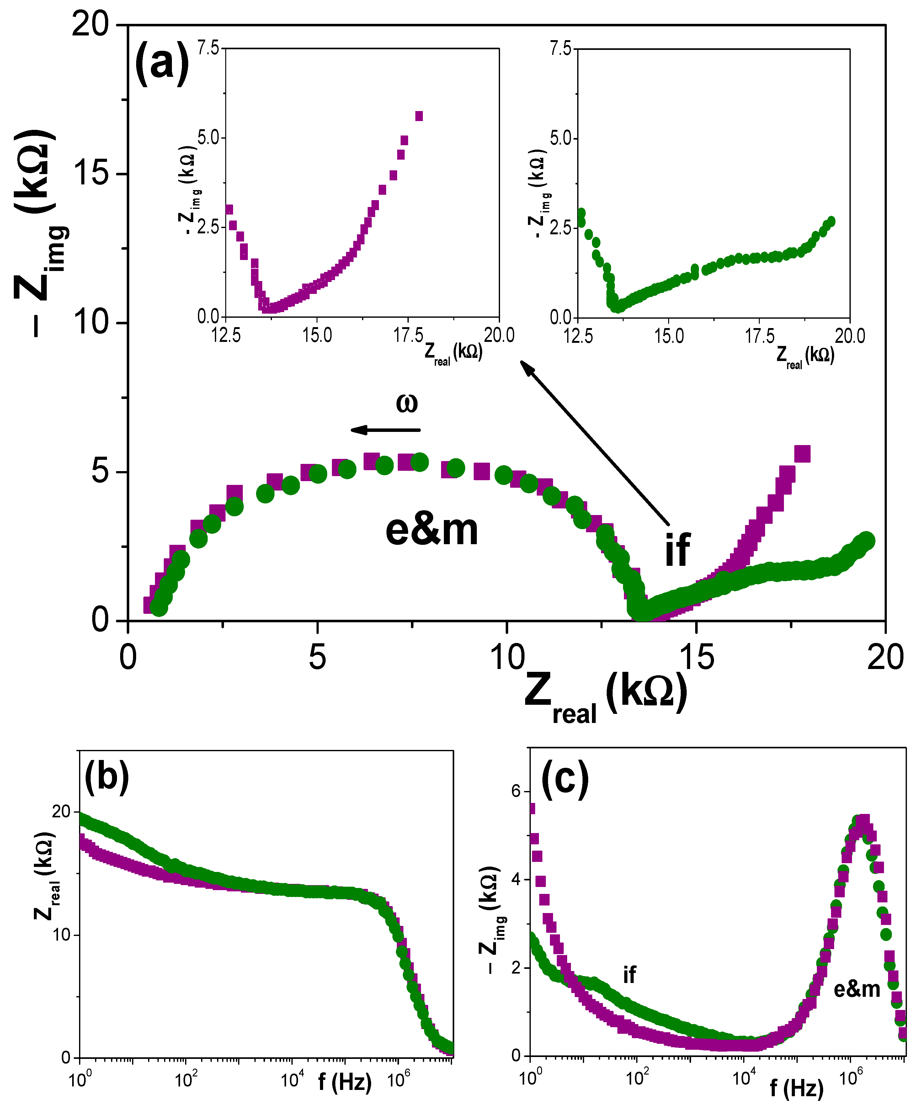
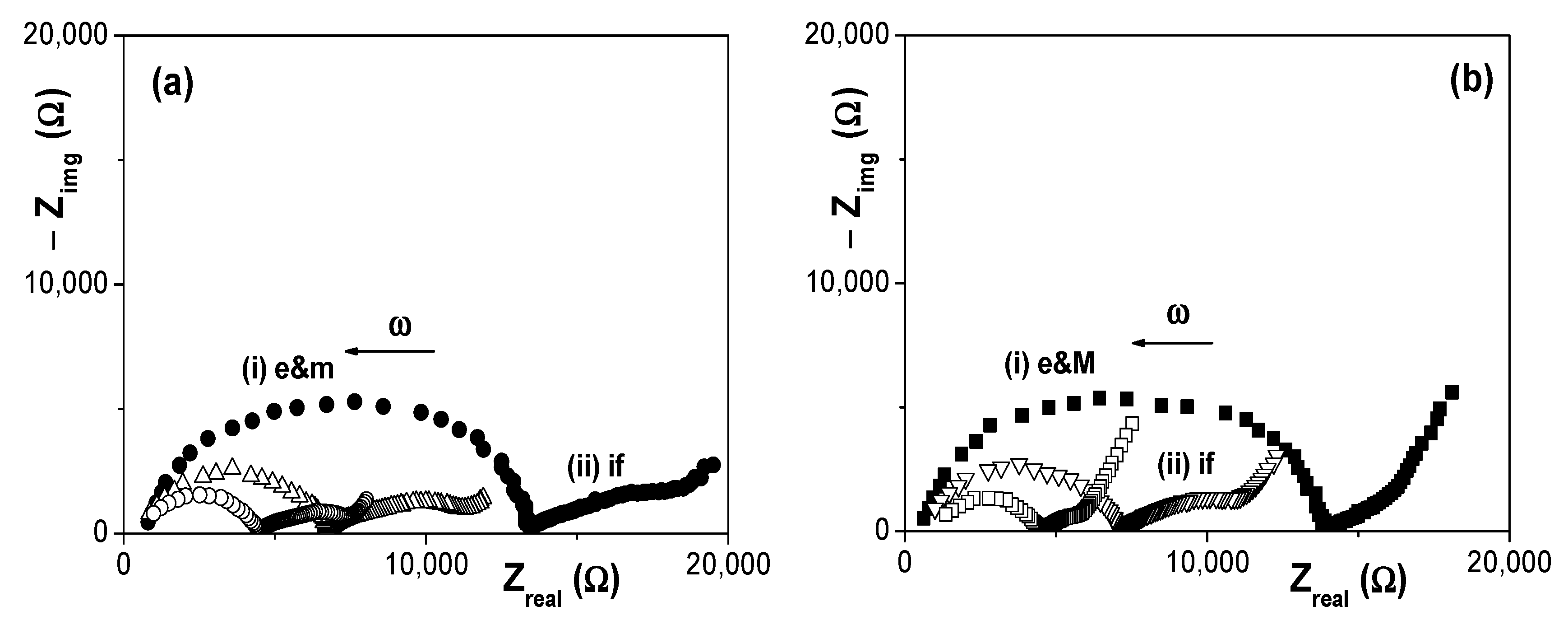
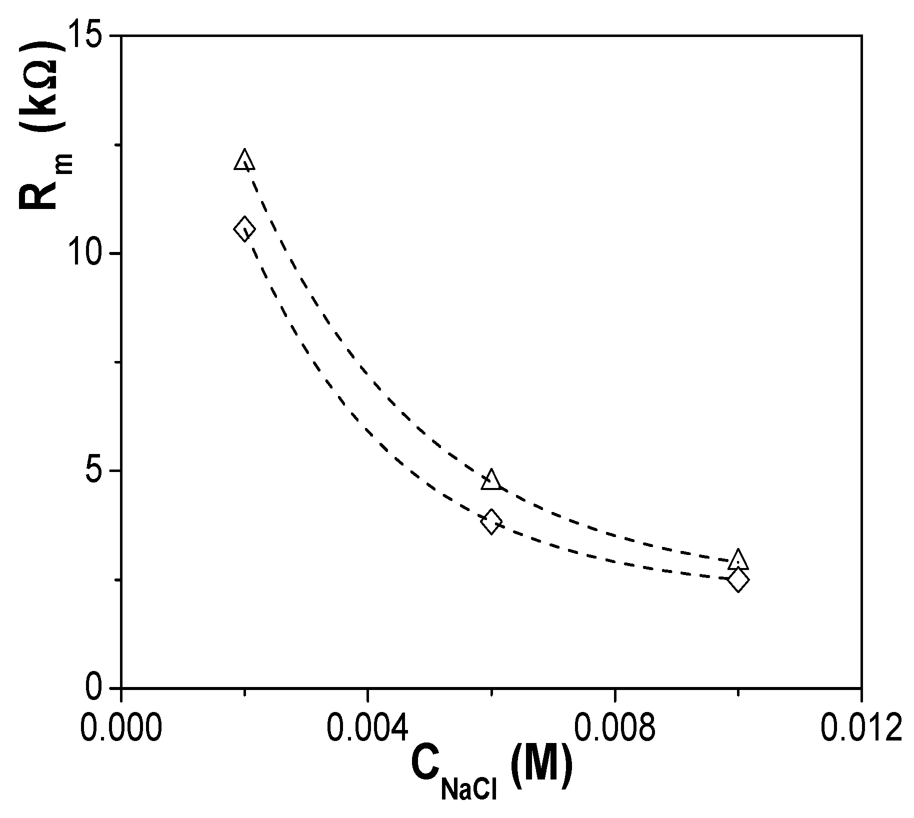
3.3. Electrochemical Impedance Spectroscopy Measurements

Once the chemical differences on the surface of Ox–SiO2/APTES and Ox–SiO2/APTES/O3 samples were established by XPS analysis, information on the effect of surface modification on diverse physicochemical parameters of interest for different sample applications (membrane, biochemical sensors, optical sensors,…) was determined. Information on electrochemical parameters involved in the transport of charged species (ions or macromolecules) across membranes is usually obtained by electrochemical measurements [7,24,37,38,39]. In particular, electrochemical impedance spectroscopy (EIS) is a technique commonly used in the electrical characterization of membranes in “working conditions”, that is, in contact and/or filled with electrolyte solutions, since it provides quantitative and qualitative information by the fitting of the impedance data using equivalent circuits as models or comparing the impedance diagrams determined for different systems [33,34,35]. Figure 6a shows the Nyquist plot (−Zimg vs. Zreal) obtained for Ox–SiO2/APTES and Ox–SiO2/APTES/O3 membranes in contact with a 0.002 M NaCl solution, where two different relaxation processes can be observed: (i) one relaxation is associated to the membrane (with the nanopores filled with the electrolyte solution) plus the electrolyte solution placed between the membrane surface and the electrodes (denominated e&m), and (ii) the other relaxation corresponds to the electrolyte/membrane interface (if) [34,35,40,41]. As it can be observed, the e&m contribution is practically coincident for both membranes, which is an indication of their geometrical similarity and the very low electrical effect caused by APTES or APTES/O3 modifications in the bulk membrane, but clear changes exist in the electrolyte/membrane interfacial region in agreement with superficial changes proposed in the scheme indicated in Figure 1 and obtained by XPS analysis. These two aspects can also be observed in the Bode plots shown in Figure 6b (Zreal vs. frequency) and Figure 6c (−Zimg vs. frequency).
The effect of electrolyte solution concentration on EIS data is clearly shown in Figure 7, where a comparison of Nyquist plots obtained for both membranes at the three NaCl concentrations studied (2 × 10⁻³ M, 6 × 10⁻³ M and 1 × 10⁻² M) is presented. As it can be observed, the membrane plus electrolyte e&m contribution, which corresponds to a slightly depressed semicircle as a result of juxtaposition of two relaxation process (one associated to the membrane and other to the electrolyte) is significantly dependent on solution concentration and, logically it decreases with the increase of charges (ions) in solution, but solution concentration also seems to affect the interfacial part.
EIS data for the two membranes plus electrolyte e&m contribution were fitted to a series combination of two contributions: (a) a parallel association of a resistance and a capacitor for the electrolyte solution (equivalent circuit: ReCe); (b) a parallel association of a resistance and a constant phase element or equivalent capacitor (CPE: Q(ω) = Yo(ω)n, for the membrane contribution (equivalent circuit: RmQm)) [32,42]. Figure 8 shows the concentration dependence of Rm obtained for the Ox+SiO2/APTES and the Ox+SiO2/O3 membranes, where slight differences (around 15%) between both samples can be observed. Assuming similarity in pore-size/porosity of both alumina supports, in agreement with SEM results, Rm differences might be associated to the particular electrical surface characteristic related to the different modifying layer of each membrane.

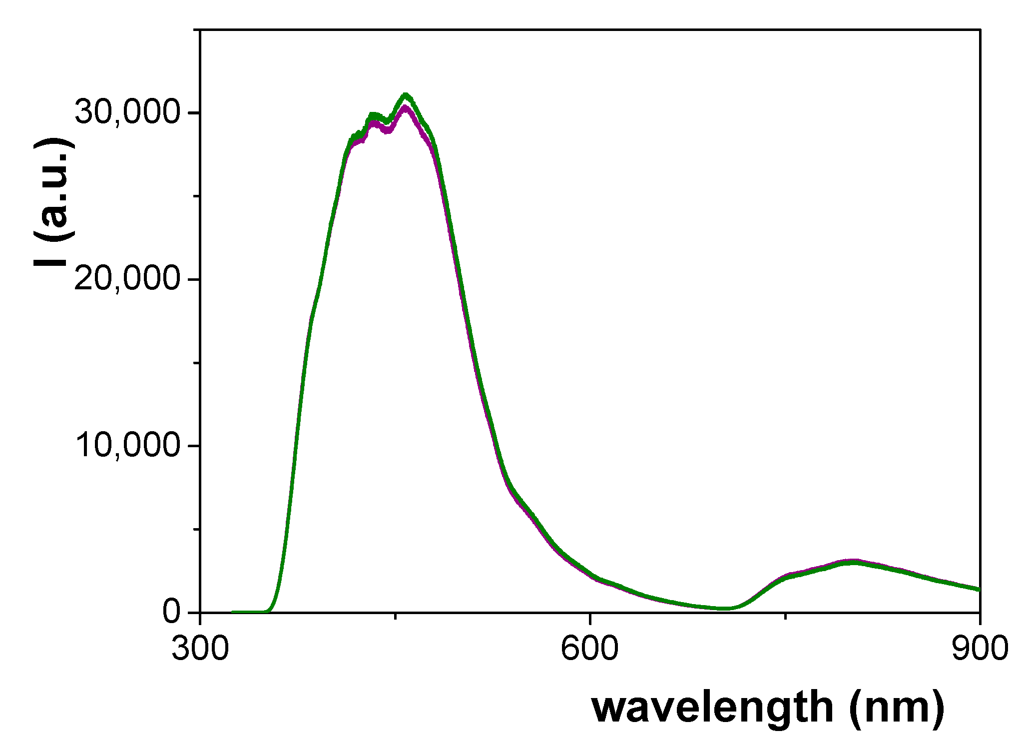
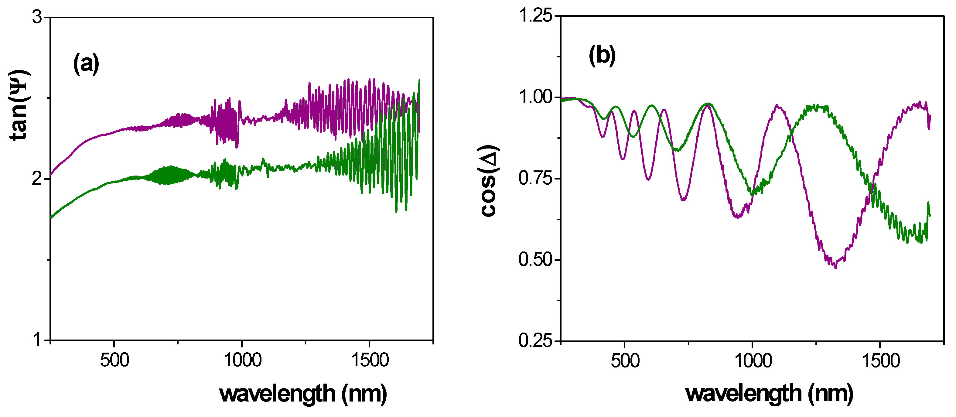
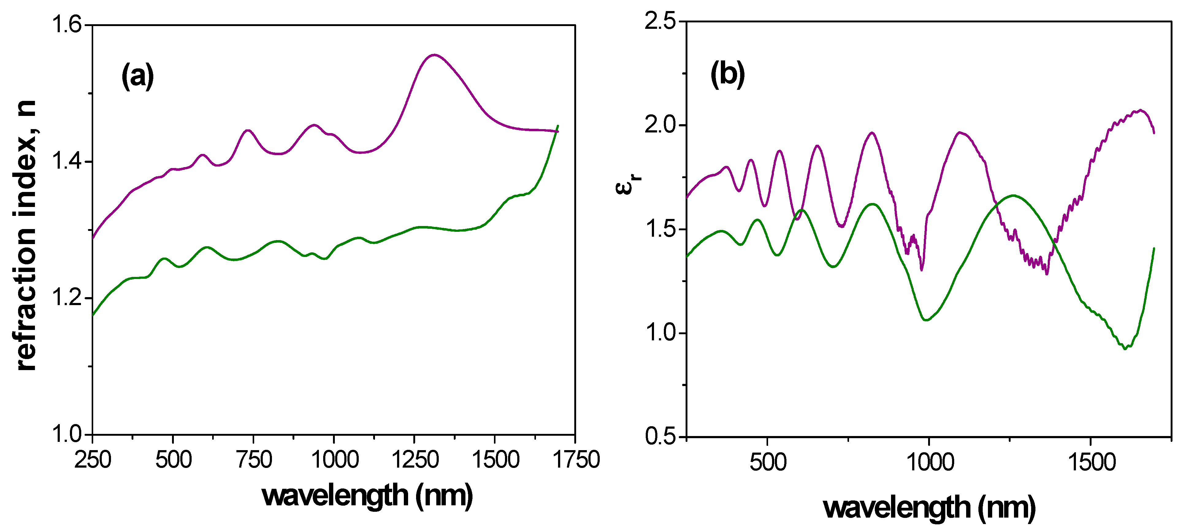
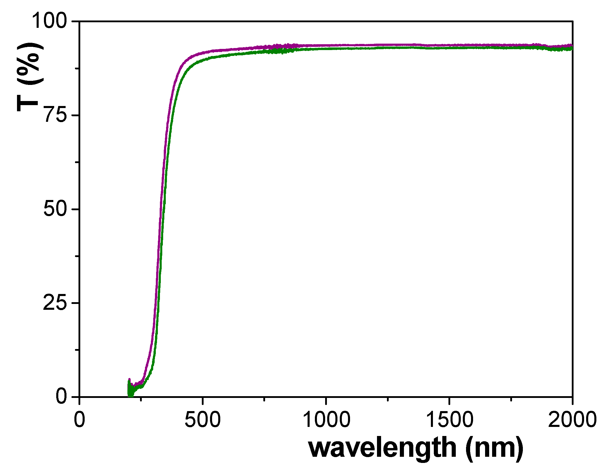
3.4. Optical Characterization

Optical techniques are of great interest in the characterization of materials due to their non-invasive and non-destructive character. In particular, spectroscopic ellipsometry has already demonstrated their suitability for characterization of nanoporous alumina membranes with different pore size, porosity or structure [43], but also for biosensors characterization [44], while light transmission spectra allows estimation of differences in both geometrical parameters (pore-size/porosity) and surface material of analyzed samples [8,12]. Moreover, a particular property of nanoporous alumina structures (NPASs) obtained by the two-step anodization method such as their potoluminescence (PL) character, which is associated to the ionized oxygen vacancies and the carboxylate from the electrolyte solution incorporated into the NPAS during the fabrication process has also been reported [45,46,47].
Figure 9 shows a comparison of the PL spectra obtained for the Ox+SiO2/APTES and Ox+SiO2/APTES/O3 membranes, where the similarity of the curves obtained for both samples, which is associated to alumina support bulk phase as it was indicated above, is very significant. In fact, the PL spectra of nanoporous alumina structures seems to be related to the incorporation of impurities to the structure of anodic alumina, which is strongly dependent on the fabrication parameters (anodization voltage, electrolyte, thermal treatment,…) [48,49]. In particular, an increase in the intensity of the PL curve as well as a shift of the wavelength value associated to the maximum of the curve with the increase of pore size have already been reported for membranes fabricated using oxalic acid as electrolyte [50]. Consequently, the likeness of both PL curves can be considered as a confirmation of alumina support similarity.
A comparison of transmission spectra for both types of NPASs, Ox–SiO2/APTES and Ox–SiO2/APTES/O3 samples, is shown in Figure 10, where two main aspects, the slight difference between both curves for the whole range of wavelength and the high transparency of both analyzed samples, can be observed. With respect to this latter point, a comparison between the transmittance spectra for diverse alumina-based structures obtained after surface coverage by ALD technique with different metal oxides, and consequently with different material surface but similar geometrical parameters, has been already reported in previous works [8,12] and it is shown as Supplementary Information (Figure S1). These results demonstrate the significant effect of sample material on light transmittance, showing values of around 90% even for samples/membranes with reduced free volume (10–13 nm pore size and 4–6% porosity). This higher influence observed in the case of those nanoporous membranes is due to the peculiar optical properties exhibited by anodic alumina together with these coming from the different ALD layers further deposited on it, which become them in outstanding materials for optical and photonic applications [51].
In the case of uncoated NPASs, noticeable changes in transmittance spectra have been reported among samples synthesized under modulated anodic electrochemical conditions, i.e., temperature, anodic voltage, etc., but these modifications are related to the formation of Distributed Bragg reflectors (DBR) due to periodic modulation of the synthesis conditions, which in turn results in periodic variations in the morphological parameter of alumina, namely pore size and porosity [52,53].
With respect to the differences exhibited by the transmittance curves of the analyzed samples, the following transparency percentage values at three given wavelengths, 400 nm, 800 nm and 2000 nm, were obtained: 81.7%, 92.4% and 92.7% for Ox–SiO2/APTES membrane, but 86.1%, 93.4 and 93.6% for Ox–SiO2/APTES/O3 one. These results indicate a difference between both samples for both extremes of the visible region of around 5% and 1%, respectively, but a practically constant difference of 1% for the near infrared region (800–2000 nm), which seems to indicate that transmission difference is more probably related to membrane material change due to APTES or APTES/O3 modification than to geometrical effects. On the other hand, band gap value for Ox–SiO2/APTES and Ox–SiO2/APTES/O3 samples hardy differ one from the other (298 nm and 286, respectively), and they are similar to that determined for a SiO2-covered nanoporous alumina structure obtained also using 0.3 M oxalic acid solution and the same anodization voltage in the two-step process (288 nm [8,12]); although these values are higher than that referred for pure SiO2 (120–155 nm, [54]) due to the presence of other modifying elements and/or impurities on samples surfaces, according to XPS results.
Spectroscopic ellipsometry (SE) is an optical technique used for the characterization of thin films and membranes able to determine changes associated to bulk phase or surface modifications [8,12,55,56]. SE measures changes in light polarization due to its reflection/transmission across a solid structure by considering two characteristic parameters, angles Ψ and Δ, which are related with differential changes in amplitude and phase between light waves through the Fresnel reflection coefficients ratio, rs and rp, of polarized light (s for perpendicular and p for parallel) by [57]:
tan(Ψ)eiΔ = rp/rs
A comparison of wavelength dependence of both experimental parameters for Ox–SiO2/APTES and Ox–SiO2/APTES/O3 samples is shown in Figure 11, where the interference fringes in tan ψ exhibited by both samples at high wavelength values are an indication of high sample transparency [58], in agreement with transmittance results already indicated. On the other hand, the oscillatory character of cos(Δ) has already been reported in the literature for anodized nanoporous alumina structures or membranes and it is related with sample pore size, surface impurities and roughness [58,59,60], while the effect of material surface on tan(Ψ) values for ALD modified NPASs has already been reported [8,12].
From experimental Ψ and Δ values, using a Cauchy dispersion model relation [61] to describe the dependence of the refractive index on the wavelength, different optical characteristic parameters such as the refractive index (n) or the dielectric constant (ε) (ε = (n + i·k)2, where k represents the extinction coefficient) can be determined [57]). Figure 12 shows a comparison of wavelength dependence for the refractive index (Figure 12a) and the real part of the dielectric constant (Figure 12b) for Ox–SiO2/APTES and Ox–SiO2/APTES/O3 samples, where differences depending on surface modification and optical regions are obtained. In fact, curves shape in visible region are rather similar, with higher variation in the near infrared region.
Average values of refraction index and dielectric constant for the whole range of wavelength as well as for visible and near infrared regions were determined for comparison reason, and these results are indicated in Table 3. A comparison of the <n> value shown in Table 3 with that referred for APTES indicates a reduction of 10% (nAPTES = 1.423 [62]), or 12% in the case of SiO2 thin film (nSiO2 = 1.46) [63]. On the other hand, ratio of refraction index and dielectric constant average values determined for both samples are practically independent of wavelength interval, being <n>Ox+SiO2/APTES/<n>Ox+SiO2/APTES/O3 ~ 0.9 and <εr>Ox+SiO2/APTES/<εr>Ox+SiO2/APTES/O3 ~ 0.8, proving evidence of surface effect difference associated to samples modification. Furthermore, the possibility of performing in-situ SE measurements during ALD deposition in both, custom-made and commercial devices, provides not only an accurate monitoring of the deposited film thickness and growth mechanisms, but also a powerful tool to determine film optical properties, including the possibility to tune at will some physical parameters of the samples such as the refraction index [64,65,66].

4. Conclusions

Deposition of SiO2 on a nanoporous alumina support by thermal ALD using a self-catalytic reaction based on 3-aminopropyltriethoxysilane (APTES), water, and ozone as precursors, in a three-step reaction sequence at low growth temperature, allows us to provide to the nanoporous support different surface functional groups (Ox+SiO2/APTES and Ox+SiO2/APTES/O3 samples), which might be of interest in different applications such as optical or electrochemical sensors, membranes or nanofluidic. XPS analysis was used for estimation of chemical surface modification, while spectroscopic ellipsometry measurements indicate changes in optical properties such as refractive index and dielectric constant, because of the difference in the surface functional groups, which enables in-situ monitoring ALD growth. Surface chemical modification also seems to affect interfacial effects when the studied samples are in contact with electrolyte solutions according to electrochemical spectroscopy results. However, surface modification hardly affects to characteristics of anodic alumina related to bulk support properties such as their photoluminescence and morphological parameters (pore diameter and porosity) taking into account the similarity exhibited by SEM micrographs and PL curves obtained for Ox+SiO2/APTES and Ox+SiO2/APTES/O3 samples.

Supplementary Materials

The following are available online at https://www.mdpi.com/article/10.3390/ma14175052/s1, Figure S1: Transmission spectra for different nanoporous alumina-based structures with similar pore size (9 ± 2) nm and porosity (7 ± 2)%, but different coating layers.

Author Contributions

Conceptualization, V.M.P. and J.B.; methodology, A.S.G. and V.V.; validation, V.M.P., V.V. and J.B.; formal analysis, A.L.C. and M.d.V.M.d.Y.; investigation, A.S.G., V.V., A.L.C., and M.d.V.M.d.Y.; writing—original draft preparation, V.V. and J.B.; writing—review and editing, A.S.G. and V.M.P.; visualization, A.S.G.; supervision, J.B. and V.M.P.; funding acquisition, V.M.P. All authors have read and agreed to the published version of the manuscript.

Funding

This research was funded by Instituto de Salud Carlos III (ISCIII), under grant number FISS-19-DTS19/00088.

Institutional Review Board Statement

Not Applicable.

Informed Consent Statement

Not Applicable.

Data Availability Statement

Not Applicable.

Acknowledgments

Authors would like to acknowledge the technical support by the Scientific-Technical services of the University of Oviedo and the Bioinnovation Center (Málaga University).

Conflicts of Interest

The authors declare no conflict of interest.

References

  1. Suntola, T.; Antson, J. Method for Producing Compound Thin Films. Patent 4058430, 15 November 1977. [Google Scholar]
  2. Hyvärinen, J.; Sonninen, M.; Törnqvist, R. Mass spectrometry study of ZnS atomic layer epitaxy process. J. Cryst. Growth 1988, 86, 695–699. [Google Scholar] [CrossRef]
  3. Hunter, A.; Kitai, A.H. A novel atmospheric pressure technique for the deposition of ZnS by atomic layer epitaxy using dimethylzinc. J. Cryst. Growth 1988, 91, 111–118. [Google Scholar] [CrossRef]
  4. Knez, M.; Nielsch, K.; Niinistö, L. Synthesis and Surface Engineering of Complex Nanostructures by Atomic Layer Deposition. Adv. Mater. 2007, 19, 3425–3438. [Google Scholar] [CrossRef]
  5. George, S.M. Atomic Layer Deposition: An Overview. Chem. Rev. 2010, 110, 111–131. [Google Scholar] [CrossRef] [PubMed]
  6. Spende, A.; Sobel, N.; Lukas, M.; Zierold, R.; Riedl, J.C.; Gura, L.; Schubert, I.; Montero Moreno, J.M.; Nielsch, K.; Stühn, B.; et al. TiO2, SiO2, and Al2O3 coated nanopores and nanotubes produced by ALD in etched ion-track membranes for transport measurements. Nanotechnology 2015, 26, 335301. [Google Scholar] [CrossRef] [Green Version]
  7. Vega, V.; Gelde, L.; González, A.S.; Prida, V.M.; Hernando, B.; Benavente, J. Diffusive transport through surface functionalized nanoporous alumina membranes by atomic layer deposition of metal oxides. J. Ind. Eng. Chem. 2017, 52, 66–72. [Google Scholar] [CrossRef]
  8. Cuevas, A.L.; Martínez de Yuso, M.V.; Gelde, L.; Gonzalez, A.S.; Vega, V.; Prida, V.M.; Benavente, J. Chemical, optical and transport characterization of ALD modified nanoporous alumina based structures. J. Ind. Eng. Chem. 2020, 91, 139–148. [Google Scholar] [CrossRef]
  9. Masuda, H.; Fukuda, K. Ordered Metal Nanohole Arrays Made by a Two-Step Replication of Honeycomb Structures of Anodic Alumina. Science 1995, 268, 1466–1468. [Google Scholar] [CrossRef] [PubMed]
  10. Lee, W.; Park, S.J. Porous Anodic Aluminum Oxide: Anodization and Templated Synthesis of Functional Nanostructures. Chem. Rev. 2014, 114, 7487–7556. [Google Scholar] [CrossRef] [PubMed]
  11. Gelde, L.; Cuevas, A.L.; Martínez de Yuso, M.D.V.; Benavente, J.; Vega, V.; González, A.S.; Prida, V.M.; Hernando, B. Influence of TiO2-Coating Layer on Nanoporous Alumina Membranes by ALD Technique. Coatings 2018, 8, 60. [Google Scholar] [CrossRef] [Green Version]
  12. Cuevas, A.L.; Martínez de Yuso, M.V.; Vega, V.; González, A.S.; Prida, V.M.; Benavente, J. Influence of ALD coating layers on the optical properties of nanoporous alumina-based structures. Coatings 2019, 9, 43. [Google Scholar] [CrossRef] [Green Version]
  13. Kumeria, T.; Santos, A.; Losic, D. Nanoporous Anodic Alumina Platforms: Engineered Surface Chemistry and Structure for for Optical Sensing Applications. Sensors 2014, 14, 11878–11918. [Google Scholar] [CrossRef] [Green Version]
  14. Rajeev, G.; Xifre-Perez, E.; Prieto Simon, B.; Cowin, A.J.; Marsal, L.F.; Voelcker, N.H. A label-free optical biosensor based on nanoporous anodic alumina for tumour necrosis factor-alpha detection in chronic wounds. Sens. Actuators B Chem. 2018, 257, 116–123. [Google Scholar] [CrossRef]
  15. Kageyama, N.; Takagaki, A.; Sugawara, T.; Kikuchi, R.; Oyama, S.T. Synthesis and characterization of a silica-alumina composite membrane and its application in a membrane reactor. Sep. Purif. Technol. 2018, 195, 437–445. [Google Scholar] [CrossRef]
  16. Ferguson, J.D.; Smith, E.R.; Weimer, A.W.; George, S.M. ALD of SiO2 at Room Temperature Using TEOS and  H2O  with  NH3 as the Catalyst. Electrochem. Soc. 2004, 151, G528. [Google Scholar] [CrossRef]
  17. Hirose, F.; Kinoshita, Y.; Shibuya, S.; Miya, H.; Hirahara, K.; Kimura, Y.; Niwano, M. Atomic-Layer-Deposition of SiO2 with Tris(Dimethylamino)Silane (TDMAS) and Ozone Investigated by Infrared Absorption Spectroscopy. ECS Trans. 2008, 13, 171. [Google Scholar] [CrossRef]
  18. Burton, B.B.; Kang, S.W.; Rhee, S.W.; George, S.M. SiO2 Atomic Layer Deposition Using Tris(dimethylamino)silane and Hydrogen Peroxide Studied by in Situ Transmission FTIR Spectroscopy. J. Phys. Chem. C 2009, 113, 8249–8257. [Google Scholar] [CrossRef]
  19. Kim, J.K.; Jin, K.; Jung, J.; Rha, S.K.; Lee, W.J. Atomic layer deposition of SiO2 thin films using tetrakis(ethylamino)silane and ozone. J. Nanosci. Nanotechnol. 2012, 12, 3589–3592. [Google Scholar] [CrossRef] [PubMed]
  20. Pfeiffer, K.; Shestaeva, S.; Bingel, A.; Munzert, P.; Ghazaryan, L.; van Helvoirt, C.; Kessels, W.M.M.; Sanli, U.T.; Grévent, C.; Schütz, G.; et al. Comparative study of ALD SiO2 thin films for optical applications. Opt. Mater. Express 2016, 663, 255642. [Google Scholar]
  21. Nam, T.; Lee, H.; Choi, T.; Seo, S.; Yoon, C.M.; Choi, Y.; Jeong, H.; Lingam, H.K.; Chitturi, V.R.; Korolev, A.; et al. Low-temperature, high-growth-rate ALD of SiO2 using aminodisilane precursor. Appl. Surf. Sci. 2019, 485, 381–390. [Google Scholar] [CrossRef]
  22. Hiller, D.; Zierold, R.; Bachmann, J.; Alexe, M.; Yang, Y.; Gerlach, J.W.; Stesmans, A.; Ji-Vanescu, M.; Müller, U.; Vogt, J.; et al. Low temperature silicon dioxide by thermal atomic layer deposition: Investigation of material properties. J. Appl. Phys. 2010, 107, 064314. [Google Scholar] [CrossRef] [Green Version]
  23. Bachmann, J.; Zierold, R.; Chong, Y.T.; Hauert, R.; Sturm, C.; Schmidt-Grund, R.; Rheinländer, B.; Grundmann, M.; Gösele, U.; Nielsch, K. A Practical, Self-Catalytic, Atomic Layer Deposition od Silicon Dioxide. Angew. Chem. Int. Ed. 2008, 47, 6177–6179. [Google Scholar] [CrossRef] [PubMed]
  24. Romero, V.; Vega, V.; Garcia, J.; Zierold, R.; Nielsch, K.; Prida, V.M.; Hernando, B.; Benavente, J. Changes in Morphology and Ionic transport Induced by ALD SiO2 Coating of Nanoporous Alumina Membanes. ACS Appl. Mater. Interfaces 2013, 5, 3556–3564. [Google Scholar] [CrossRef] [PubMed]
  25. Hsiao, V.K.S.; Waldeisen, J.R.; Zheng, Y.; Lloyd, P.F.; Bunning, T.J.; Huang, T.J. Aminopropyltriethoxysilane (APTES)-functionalized nanoporous polymeric gratings: Fabrication and application in biosensing. J. Mater. Chem. 2007, 17, 4896–4901. [Google Scholar] [CrossRef]
  26. Nayak, N.; Huertas, R.; Crespo, J.G.; Portugal, C.A.M. Surface modification of alumina monolithic columns with 3-aminopropyltetraethoxysilane (APTES) for protein attachment. Sep. Purif. Technol. 2019, 229, 115674. [Google Scholar] [CrossRef]
  27. Kumeria, T.; Santos, A.; Losic, D. Ultrasensitive nanoporous interferometric sensor for label-free detection of gold (III) ions. ACS Appl. Mater. Interfaces 2013, 5, 11783–11790. [Google Scholar] [CrossRef] [PubMed]
  28. Santos, A.; Kumeria, T.; Losic, D. Optically optimized photoluminescent and interferometric biosensors based on nanoporous anodic alumina: A comparison. Anal. Chem. 2013, 85, 7904–7911. [Google Scholar] [CrossRef]
  29. Rai, V.R.; Agarwal, S. Mechanism of Self-catalytic Atomic Layer Deposition of Silicon Dioxide Using 3-Aminopropyl Triethoxysilane, Water, and Ozone. Chem. Mater. 2011, 23, 2312–2316. [Google Scholar] [CrossRef]
  30. Schneider, C.A.; Rasband, W.S.; Eliceiri, K.W. NIH Image to ImageJ: 25 years of image analysis. Nat. Methods 2012, 9, 671–675. [Google Scholar] [CrossRef] [PubMed]
  31. Briggs, D.; Seah, M.P. Practical Surface Analysis, Vol1: Auger and X-ray Photoelectron Spectroscopy, 2nd ed.; Jon Wiley & Sons: Chischester, UK, 1995. [Google Scholar]
  32. Macdonald, J.R.; Johnson, W.B. Fundamentals of Impedance Spectroscopy. In Impedance Spectroscopy: Theory, Experiment, and Applications, 3rd ed.; Barsoukov, E., Ed.; Wiley Online Library: Hoboken, NJ, USA, 2018. [Google Scholar] [CrossRef]
  33. Benavente, J.; Rodriguez-Castellón, E. Application of Electrochemical Impedance Spectroscopy (EIS) and X-ray Photoelectron Spectroscopy (XPS) to the Characterization of RTILs for Electrochemical Applications. In Ionic Liquids: Applications and Perspectives; Chapter 27; Kokorin, A., Ed.; InTech Publisher: London, UK, 2011; ISBN 978-953-307-248-7. [Google Scholar]
  34. Benavente, J. Use of Impedance Spectroscopy for characterization of modified membranes. In Membrane. Modification: Technology and Applications; Hilal, N., Kayet, M., Wright, C.J., Eds.; CRC Press: Boca Raton, FL, USA, 2012; ISBN 9781439866368. [Google Scholar]
  35. Benavente, J.; García, J.M.; Riley, R.; Lozano, A.E.; de Abajo, J. Sulfonated poly(ether ether sulfone). Characterization and study of dielectrical properties by impedance spectroscopy. J. Membr. Sci. 2000, 175, 43–52. [Google Scholar] [CrossRef]
  36. Moulder, J.F.; Stickl, W.F.; Sobol, P.E.; Bomben, K.D. Handbook of X-ray Photoelectron Spectroscopy; Chastain, J., Ed.; Perkin-Elmer Corporation: Minneapolis, MN, USA, 1992. [Google Scholar]
  37. Lakshminarayanaiah, N. Transport Phenomena in Membranes; Academic Press Inc.: New York, NY, USA, 1970; ISBN 9780124342507. [Google Scholar]
  38. Sbaï, M.; Fievet, P.; Szymczyk, A.; Aoubiza, B.; Vidonne, A. Streaming potential, electroviscous effect, pore conductivity and membrane potential for the determination of the surface potential of a ceramic ultrafiltration membrane. J. Membr. Sci. 2003, 215, 1–9. [Google Scholar] [CrossRef]
  39. Cen, J.; Vukas, M.; Barton, G.; Kavanagh, J.; Coster, H.G.L. Real time fouling monitoring with Electrical Impedance Spectroscopy. J. Membr. Sci. 2015, 484, 133–139. [Google Scholar] [CrossRef]
  40. Cañas, A.; Ariza, M.J.; Benavente, J. Characterization of active and porous sublayers of a composite reverse osmosis membrane by impedance spectroscopy, streaming and membrane potentials, salt diffusion and X-ray photoelectron spectroscopy measurements. J. Membr. Sci. 2001, 183, 135–146. [Google Scholar] [CrossRef]
  41. Gelde, L.; Cuevas, A.L.; Benavente, J. Influence of pore-size/porosity on ion transport and static BSA-fouling for TiO2-covered nanoporous alumina membranes. Appl. Sci. 2021, 11, 5687. [Google Scholar] [CrossRef]
  42. Benavente, J.; Ramos-Barrado, J.R.; Cabeza, A. Electrical behaviour of an inorganic film from ac and dc measurements. J. Colloid Interface Sci. 1996, 180, 116–121. [Google Scholar] [CrossRef]
  43. Cuevas, A.L.; González, A.S.; Vega, V.; Prida, V.M.; Benavente, J. Optical and Electrochemical Characterization of Nanoporous Alumina Structures: Pore Size, Porosity, and Structure Effect. Appl. Sci. 2020, 10, 4864. [Google Scholar] [CrossRef]
  44. Maciulis, V.; Malinovskis, U.; Erts, D.; Ramanavicius, A.; Ramanaviciene, A.; Balevicius, S.; Juciute, S.; Plikusiene, I. Porous Aluminium Oxide Coating for the Development of Spectroscopic Ellipsometry Based Biosensor: Evaluation of Human Serum Albumin Adsorption. Coatings 2020, 10, 1018. [Google Scholar] [CrossRef]
  45. Yamamoto, Y.; Baba, N.; Tajima, S. Colored materials and photoluminescence in anodic film on aluminium. Nature 1981, 289, 572–574. [Google Scholar] [CrossRef]
  46. Du, Y.; Cai, W.L.; Mo, C.M.; Chem, J.; Zhag, L.D.; Zhu, X.G. Preparation and photoluminescence of alumina membranes with ordered pore arrays. Appl. Phys Lett. 1999, 74, 2951–2953. [Google Scholar] [CrossRef]
  47. Sun, X.; Xu, F.; Li, Z.; Zhang, W. Photoluminescence properties of alumina membranes with ordered nanopore arrays. J. Lumin. 2006, 121, 588–594. [Google Scholar] [CrossRef]
  48. Mukhurov, N.I.; Zhvavyi, S.P.; Gasenkova, I.V.; Terekhov, S.N. Photoluminescence of F-centers in films of anodic alumina. J. Appl. Spectrosc. 2008, 75, 214–218. [Google Scholar] [CrossRef]
  49. Stojadinovic, S.; Nedic, Z.; Belca, I.; Vasilic, R.; Kasaliza, B.; Petkovic, M.; Zekovic, L.J. The effect of annealing on the photoluminescent and optical properties of porous anodic alumina films formed in sulfamic acid. Appl. Surs. Sci. 2009, 256, 763–767. [Google Scholar] [CrossRef]
  50. Santos, A.; Alba, M.; Rahman, M.M.; Formentín, P.; Ferré-Borrull, J.; Pallarès, J. Structural tuning of photoluminescence in nanoporous anodic alumina by hard anodization in oxalic and malonic acids. Nanoscale Res. Lett. 2012, 7, 228. [Google Scholar] [CrossRef] [PubMed] [Green Version]
  51. Law, C.S.; Lim, S.Y.; Abell, A.D.; Voelcker, N.H.; Santos, A. Nanoporous Anodic Alumina Photonic Crystals for Optical Chemo- and Biosensing: Fundamentals, Advances, and Perspectives. Nanomaterials 2018, 8, 788. [Google Scholar] [CrossRef] [PubMed] [Green Version]
  52. Zheng, W.J.; Fei, G.T.; Wang, B.; Zhang, L.D. Modulation of Transmission Spectra of Anodized Alumina Membrane Distributed Bragg Reflector by Controlling Anodization Temperature. Nanoscale Res. Lett. 2009, 4, 665–667. [Google Scholar] [CrossRef] [Green Version]
  53. Lim, S.Y.; Law, C.S.; Marsal, L.F.; Santos, A. Engineering of Hybrid Nanoporous Anodic Alumina Photonic Crystals by Heterogeneous Pulse Anodization. Sci. Rep. 2018, 8, 9455. [Google Scholar] [CrossRef] [PubMed]
  54. Strehlow, W.H.; Cook, E.L. Compilation of Energy Band Gaps in Elemental and Binary Compound Semiconductors and Insulators. J. Phys. Chem. Ref. Data 1973, 2, 163–199. [Google Scholar] [CrossRef] [Green Version]
  55. Algarra, M.; Cuevas, A.L.; Martínez de Yuso, M.V.; Benavente, J. Insights into the formation of an emissive CdTe-quantum-dots/cellulose hybrid film. J. Colloids Interface Sci. 2020, 579, 714–722. [Google Scholar] [CrossRef] [PubMed]
  56. Ogieglo, W.; Wormeerster, H.; Wessling, M.; Benes, N.E. Spectroscopic ellipsometry analysis of a thin film composite membrane consisting of polysulfone on a porous α-alumina support. ACS Appl. Mater. Interfaces 2012, 4, 935–943. [Google Scholar] [CrossRef]
  57. Tompkins, H.G.; McGahan, W.A. Spectroscopic Ellipsometry and Reflectometry: A User’s Guide; Wiley: Hoboken, NJ, USA, 1999; ISBN 978-0-471-18172-9. [Google Scholar]
  58. Cuevas, A.L.; Campos, B.B.; Romero, R.; Algarra, M.; Vázquez, M.I.; Benavente, J. Eco-friendly Modification of a Regenerated Cellulose Based Film by Silicon, Carbon and N-doped Carbon Quantum Dots. Carbohydr. Polym. 2019, 206, 238–244. [Google Scholar] [CrossRef]
  59. Logothetidis, M.; Gioti, C. Gravalidis, Optical and electronic characterization on polymeric membranes. Synth. Met. 2003, 138, 369–374. [Google Scholar] [CrossRef]
  60. Gioti, M.; Laskarakis, A.; Logothetidis, S. IR-FUV ellipsometry studies on the optical, electronic and vibrational properties of polymeric membranes. Thin Solid Films 2004, 455–456, 283–287. [Google Scholar] [CrossRef]
  61. Fujiwara, H. Spectroscopic Ellipsometry, Principles and Applications; John Wiley & Sons, Ltd.: Hoboken, NJ, USA, 2007. [Google Scholar]
  62. Lide, D.R. CRC Handbook of Chemistry and Physics, 88th ed.; 20072008; CRC Press; Taylor & Francis: Boca Raton, FL, USA, 2007. [Google Scholar]
  63. Refractive Index of SiO2, Fused Silica, Silica, Silicon Dioxide, Thermal Oxide, ThermalOxide. Available online: www.filmetrics.com/refractive-index-database/SiO2 (accessed on 10 July 2021).
  64. Muneshwar, T.; Cadien, K. Probing initial-stages of ALD growth with dynamic in situ spectroscopic ellipsometry. Appl. Surf. Sci. 2015, 328, 344–348. [Google Scholar] [CrossRef]
  65. Kilic, U.; Mock, A.; Sekora, D.; Gilbert, S.; Valloppilly, S.; Melendez, G.; Ianno, N.; Langell, M.; Schubert, E.; Schubert, M. Precursor-surface interactions revealed during plasma-enhanced atomic layer deposition of metal oxide thin films by in-situ spectroscopic ellipsometry. Sci. Rep. 2020, 10, 10392. [Google Scholar] [CrossRef]
  66. Skopin, E.V.; Abdukayumov, K.; Younes, P.A.; Anikin, M.; Roussel, H.; Deschanvres, J.L.; Renevier, H. In situ ellipsometry monitoring of TiO2 atomic layer deposition from tetrakis(dimethylamido)titanium(IV) and H2O precursors on Si and In0.53Ga0.47As substrates. Thin Solid Films 2021, 723, 138591. [Google Scholar] [CrossRef]
Figure 1. Schematic drawing of the surface reactions taking place during the different steps in a SiO2 ALD deposition cycle: (a) APTES cycle; (b) H2O cycle and (c) O3 cycle.
Materials 14 05052 g001
Figure 2. SEM micrographs of nanoporous alumina membrane (a) as produced (Ox sample), top view and cross section (inset); (b) after ALD SiO2 deposition (Ox+SiO2), top view; (c) as produced (Ox sample), bottom view (d) after ALD SiO2 deposition (Ox+SiO2), bottom view (e) after SiO2/APTES ALD cycle (Ox+SiO2/APTES), and (f) after SiO2/APTES/O3 ALD cycle (Ox+SiO2/APTES/O3).
Materials 14 05052 g002
Figure 3. Pore diameter distribution obtained by image analysis of nanoporous alumina membranes before (Ox) and after SiO2 (Ox+SiO2), SiO2/APTES (OX+ SiO2/APTES) and SiO2 (OX+ SiO2)/APTES/O3 ALD deposition.
Materials 14 05052 g003
Figure 4. Survey XPS spectra of Ox+SiO2/APTES (green line) and Ox+SiO2/APTES/O3 (purple line) samples.
Materials 14 05052 g004
Figure 5. Carbon core level spectra (black solid line) and its deconvolution for: (a) Ox+SiO2/APTES: CA, dashed red line; CB, dashed blue line; Cc, dashed green line; (b) Ox+SiO2/APTES/O3: CA, dashed red line; CB, dashed blue line; Cc, dashed green line; CD, dashed magenta line. Oxygen core level spectra (black solid line) and its deconvolution for: (c) Ox+SiO2/APTES sample: OA, dashed blue line; OB, dashed green line; (d) Ox+SiO2/APTES/O3 sample: OA, dashed blue line; OB, dashed green line; Oc, dashed magenta line. Experimental values: red solid line; fitted values: dashed red line. (e) Nitrogen and (f) Silicon core level spectra for Ox+SiO2/APTES (green solid line) and Ox+SiO2/APTES/O3 (purple solid line) samples.
Materials 14 05052 g005
Figure 6. Comparison of impedance plots for Ox–SiO2/APTES (●) and Ox–SiO2/APTES/O3 (■) samples measured with 0.002 M NaCl solution. (a) Nyquist plot (−Zimg vs. Zreal); (b) Bode plot (Zreal vs. frequency) and (c) Bode plot (−Zimg vs. frequency).
Materials 14 05052 g006
Figure 7. Comparison of Nyquist plots obtained for three different NaCl solution concentrations. (a) Ox–SiO2/APTES membrane system: (●) 0.002 M NaCl solution, (Δ) 0.006 M NaCl solution and (o) 0.01 M NaCl solution. (b) Ox–SiO2/APTES/O3 membrane system: (■) 0.002 M NaCl solution, (▽) 0.006 M NaCl solution and (□) 0.01 M NaCl solution.
Materials 14 05052 g007
Figure 8. Membrane resistance dependence with NaCl concentration for both Ox–SiO2/APTES (◊) and Ox–SiO2/APTES/O3 (Δ) membranes.
Materials 14 05052 g008
Figure 9. Photoluminescence spectra for Ox–SiO2/APTES sample (green line) and Ox-SiO2/APTES/O3 sample (purple line).
Materials 14 05052 g009
Figure 10. Transmission spectra for Ox–SiO2/APTES sample (green line) and Ox–SiO2/APTES/O3 sample (purple line).
Materials 14 05052 g010
Figure 11. Wavelength dependence of: (a) tanΨ, (b) cosΔ, for Ox–SiO2/APTES (green line) and Ox-SiO2/APTES/O3 (purple line) samples.
Materials 14 05052 g011
Figure 12. Wavelength dependence of: (a) refractive index; (b) real part of dielectric constant. Sample Ox+SiO2/APTES: solid green line, Ox+SiO2/APTES/O3: solid purple line.
Materials 14 05052 g012
Table 1. Atomic concentration percentages of the elements found on samples surfaces *.
SampleC (%)O (%)N (%)Si (%)Al (%)
Ox+SiO2/APTES12.855.30.726.94.0
Ox+SiO2/APTES/O38.359.3-28.13.9
* Elements associated to impurities with A.C. % < 0.3 are not indicated.
Table 2. Binding energy (B.E.) of the different links, area percentages (cursive) and A.C. % after carbon (A) and oxygen (B) signals deconvolution.
(A)----
SampleCA (%)CB (%)CC (%)CD (%)
B.E. (eV)285.0286.6288.9289.4
-CC/CHCO/CN/CSiC=OO–C=O
Ox+SiO2/APTESArea %81.316.432.2-
A.C. %10.42.10.3-
Ox+SiO2/APTES/O3Area %81.713.10.74.5
A.C. %6.81.10.060.37
(B)----
SampleOA (%)OB (%)OC (%)
B.E. (eV)531.6532.6533.9
-Al–OSi–O/SiO2/O–C=O*O*–C=O
Ox+SiO2/APTESArea %10.389.7-
A.C. %5.749.6-
Ox+SiO2/APTES/O3Area %10.584.55.0
A.C. %6.250.13.0
Table 3. Average values of the refraction index, <n>, and the real part of dielectric constant, <εr>, for different wavelength intervals.
SampleOx+SiO2/APTESOx+SiO2/APTES/O3
<n> 250–1700 nm1.28 ± 0.041.43 ± 0.06
r> 250–1700 nm1.38 ± 0.201.71 ± 0.20
<n> 250–800 nm1.25 ± 0.031.38 ± 0.04
r> 250–800 nm1.46 ± 0.071.72 ± 0.10
<n> 800–1700 nm1.31 ± 0.041.46 ± 0.04
r> 800–1700 nm1.33 ± 0.231.71 ± 0.24
Publisher’s Note: MDPI stays neutral with regard to jurisdictional claims in published maps and institutional affiliations.

