
Growth and Investigation of Annealing Effects on Ternary Cd1−xMgxO Nanocomposit Thin Films

 ,
,  ,
,
Abstract
:1. Introduction
2. Experimental Procedure
2.1. Sample Preparation
2.2. Characterization Techniques
3. Results and Discussion
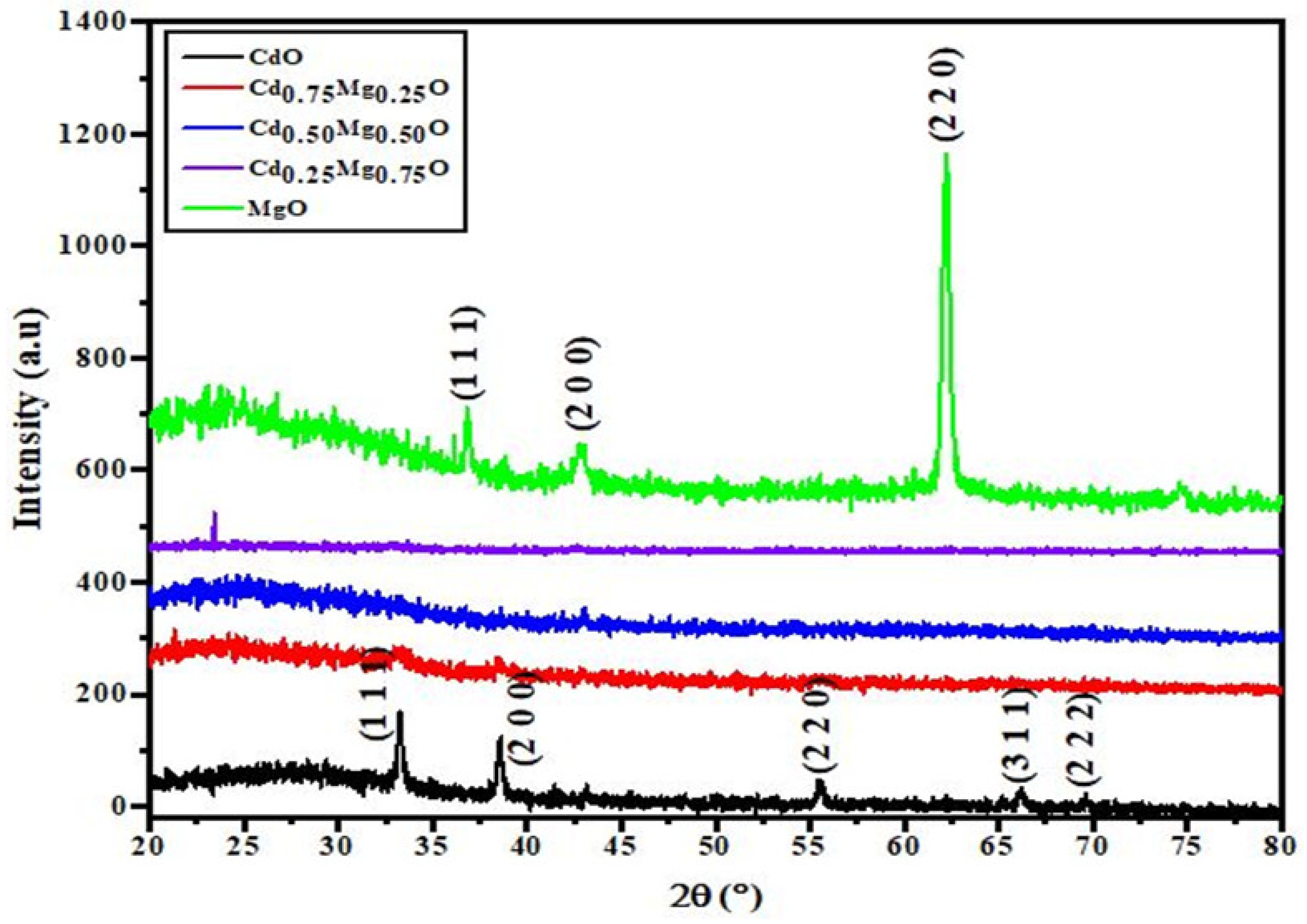
3.1. Structural Properties
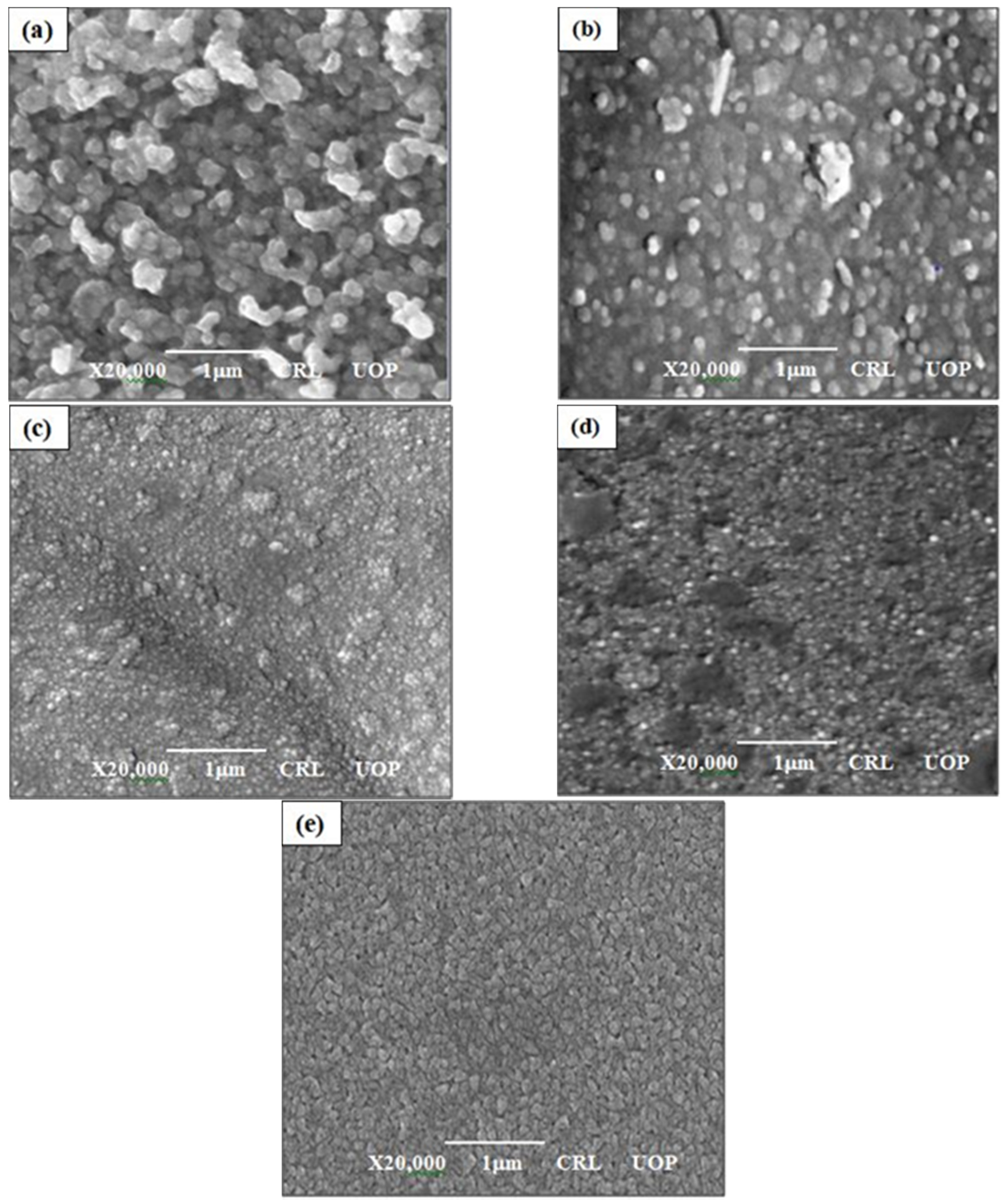
3.2. Surface Morphology
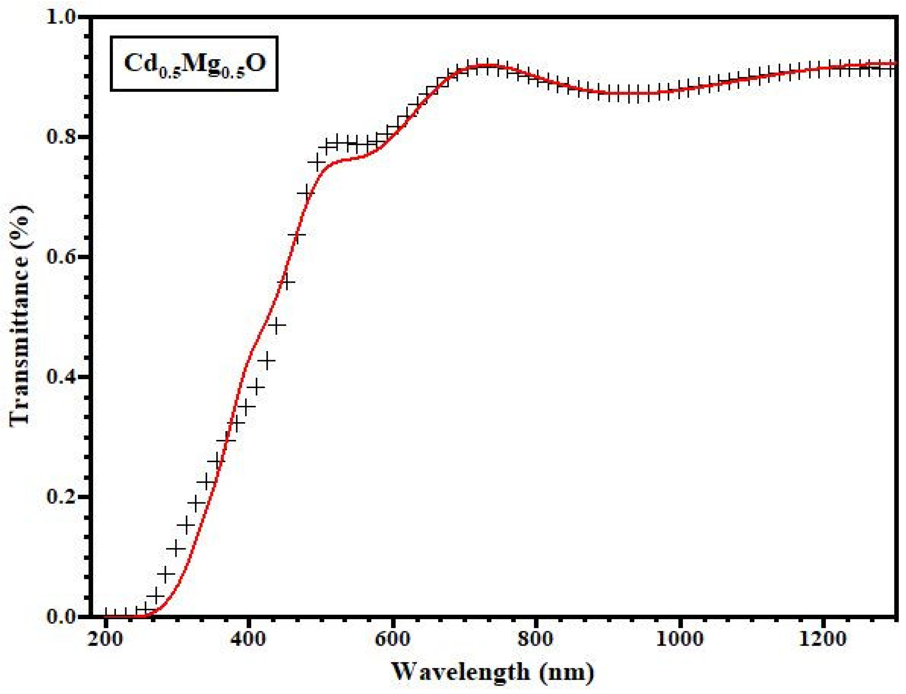
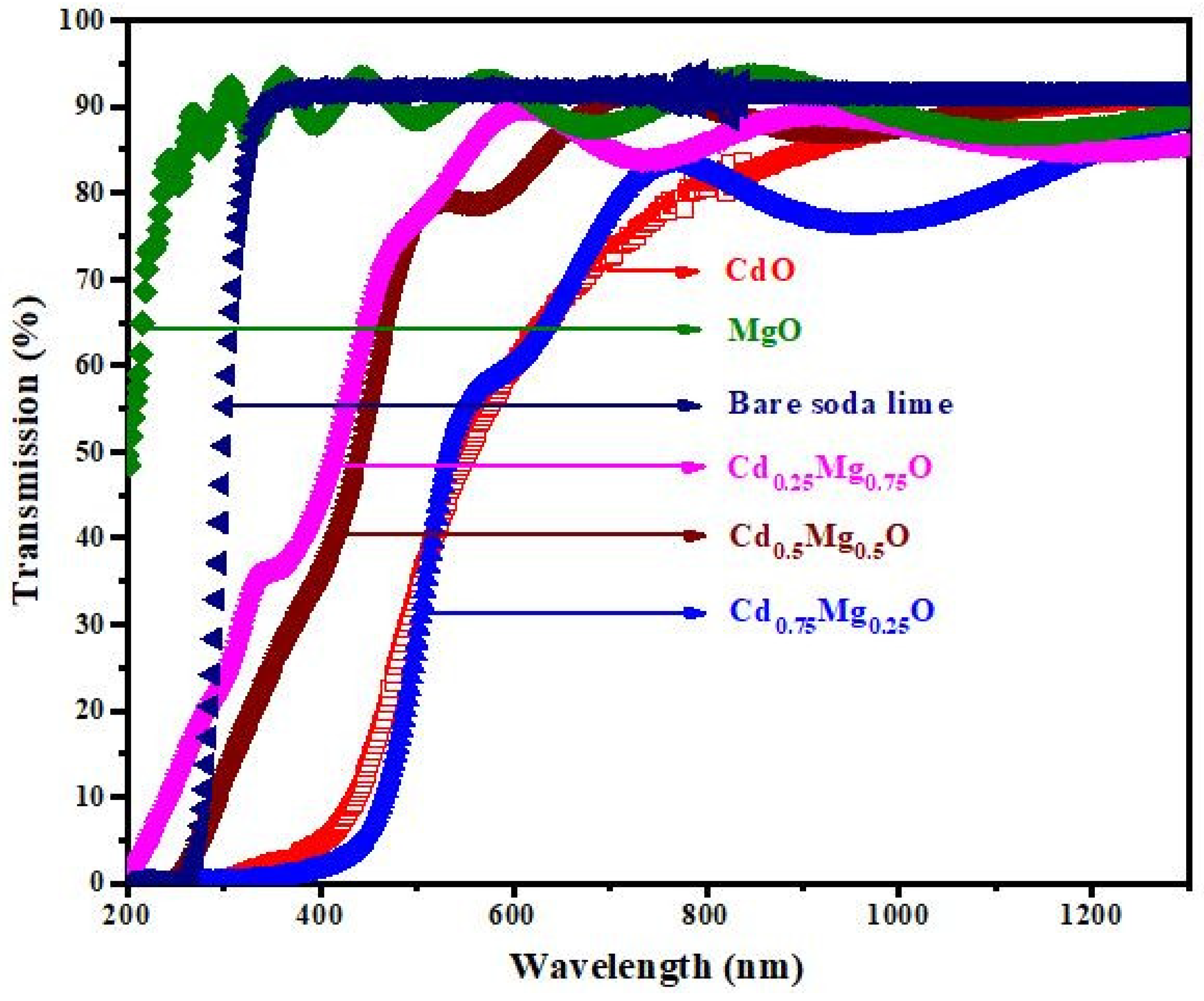
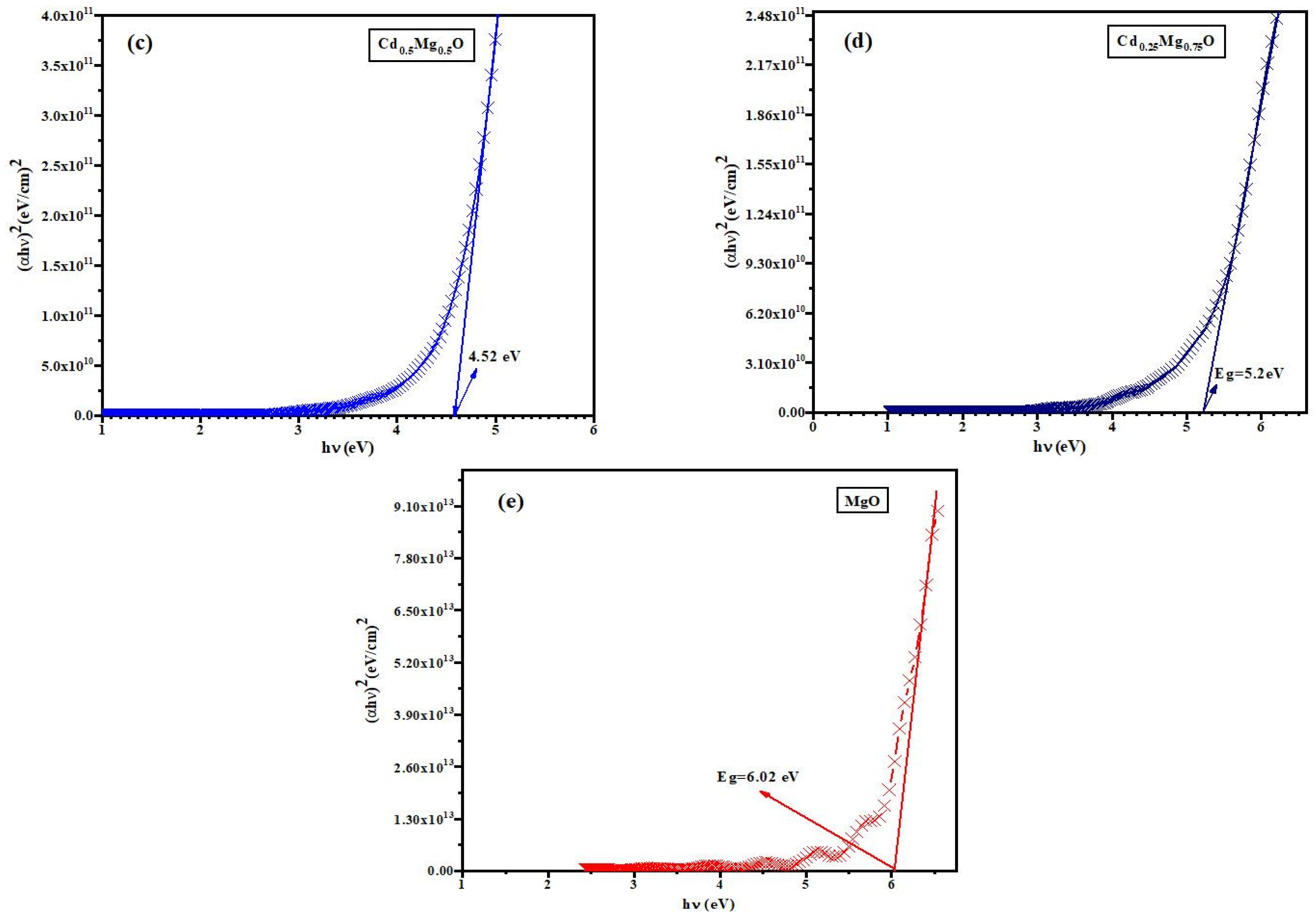
3.3. Optical Properties
- For such a type of semiconductor thin film, “T” represents the system’s typical transmittance [24]. The various variables are specified as follows: x = exp(−αd), = 4nd/, A = 16 n2s, B = (n + 1)3(n + s2), C = 2(n2 − 1)(n2 − s2), D = (n − 1)3 (n − s2). Here
- n = the film refractive index
- s = the refractive index of the glass substrate
- d = film thickness
- α = the film’s absorption coefficient
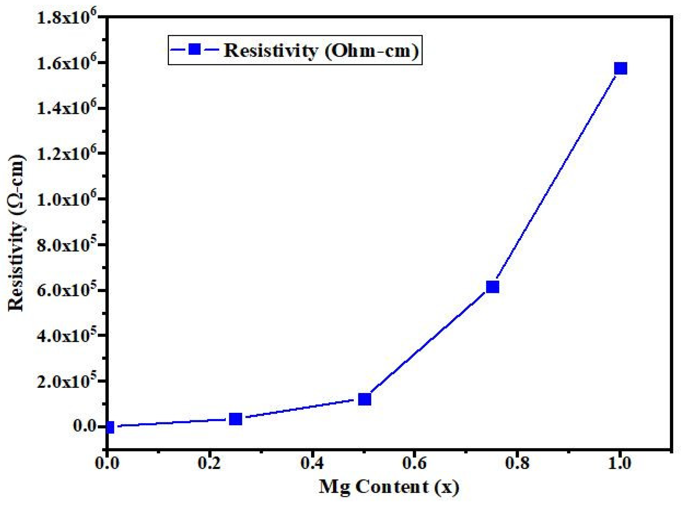
3.4. Electrical Properties
4. Conclusions
Author Contributions
Funding
Conflicts of Interest
References
- Mahmoud, W.E.; Al-Ghamdi, A.A. Synthesis of CdZnO thin film as a potential candidate for optical switches. Opt. Laser Technol. 2010, 427, 1134–1138. [Google Scholar] [CrossRef]
- Bakke, J.R.; Hägglund, C.; Jung, H.J.; Sinclair, R.; Bent, S.F. Atomic layer deposition of CdO and CdxZn1−xO films. Mater. Chem. Phys. 2013, 140, 465–471. [Google Scholar] [CrossRef]
- Huso, J.; Morrison, J.L.; Che, H.; Sundararajan, J.P.; Yeh, W.J.; McIlroy, D.; Bergman, L. ZnO and MgZnO nanocrystalline flexible films: Optical and material properties. J. Nanomater. 2011, 2011, 557–563. [Google Scholar] [CrossRef] [Green Version]
- Achary, S.R.; Agouram, S.; Sánchez-Royo, J.F.; Lopez-Ponce, M.; Ulloa, J.M.; Muñoz, E.; Muñoz-Sanjose, V. Self-assembled Mgx Zn1−xO quantum dots (0 ≤ x ≤ 1) on different substrates using spray pyrolysis methodology. CrystEngComm 2013, 15, 182–191. [Google Scholar] [CrossRef] [Green Version]
- Ashraf, M.; Akhtar, S.M.J.; Qayyum, A. Characterization of ternary MgxZn1−xO thin films deposited by electron beam evaporation. Mater. Sci. Semicond. Process. 2012, 15, 251–257. [Google Scholar] [CrossRef]
- Champness, C.H.; Xu, Z. Effect of CdO interlayer on electrical characteristics in SeBi diodes. Appl. Surf. Sci. 1998, 123, 485–489. [Google Scholar] [CrossRef]
- Yildirim, M.A.; Ates, A. Structural, optical and electrical properties of CdO/Cd (OH)2 thin films grown by the SILAR method. Sens. Actuators A 2009, 155, 272–277. [Google Scholar] [CrossRef]
- Vossen, J.L.; Hass, I.G.; Francombe, M.H.; Hoffman, R.W. (Eds.) Physics of Thin Solid Films; Academic Press: Cambridge, MA, USA, 1977; p. 1. [Google Scholar]
- Subrayaman, T.K.; Krishna, B.R.; Uthanna, S.; Naidu, B.S.; Reddy, P.J. Influence of oxygen pressure on the physical properties of dc magnetron reactive sputtered cadmium oxide films. Vacuum 1997, 48, 565. [Google Scholar] [CrossRef]
- Dantus, C.; Rusu, G.G.; Dobromir, M.; Rusu, M. Preparation and characterization of CdO thin films obtained by thermal oxidation of evaporated Cd thin films. Appl. Surface Sci. 2008, 255, 2665–2670. [Google Scholar] [CrossRef]
- Saha, B.; Thapa, R.; Chattopadhyay, K.K. Bandgap widening in highly conducting CdO thin film by Ti incorporation through radio frequency magnetron sputtering technique. Solid State Commun. 2008, 145, 33–37. [Google Scholar] [CrossRef]
- Lee, Y.; Liu, C.P.; Yu, K.M.; Walukiewiew, W. Engineering electronic band structure of Indium-doped Cd1−xMgxO alloys for solar power conversion applications. Energy Technol. 2018, 6, 122–126. [Google Scholar] [CrossRef] [Green Version]
- Flores-Mendoza, M.A.; Castanedo-Perez, R.; Torres-Delgado, G.; Rodriguez-Fragoso, P.; Mondoza-Alvarez, J.G. Photoluminescence in undoped (CdO)1−x–(InO3/2)x thin films at room temperature, 0 ≤ x ≤ 1. J. Lumin. 2013, 135, 133–138. [Google Scholar] [CrossRef]
- Deokate, R.J.; Pawar, S.M.; Moholkar, A.V.; Sawant, V.S.; Pawar, C.A.; Bhosale, C.H.; Rajpure, K.Y. Spray deposition of highly transparent fluorine doped cadmium oxide thin films. Appl. Surf. Sci. 2008, 254, 2187–2195. [Google Scholar] [CrossRef]
- De Leon-Gutierrez, L.R.; Cayente-Remero, J.J.; Peza-Tapia, J.M.; Barrera-Calva, E.; Martinez-Flores, J.C.; Ortega-Lopez, M. Some physical properties of Sn-doped CdO thin films prepared by chemical bath deposition. Mater. Lett. 2006, 60, 3866–3870. [Google Scholar] [CrossRef]
- Usharani, K.; Balu, A.R. Structural, optical, and electrical properties of Zn-doped CdO thin films fabricated by a simplified spray pyrolysis technique. Acta Metall. Sin. 2015, 28, 64–71. [Google Scholar] [CrossRef] [Green Version]
- Bonhaliliba, M.; Benouis, C.E.; Tiburcio-Silver, A.; Yakuphanoglu, F.; Avila-Garciad, A.; Tavira, A.; Trujillo, R.R.; Mouffak, Z. Luminescence and physical properties of copper doped CdO derived nanostructures. J. Lumin. 2012, 132, 2653–2658. [Google Scholar] [CrossRef]
- Pan, L.L.; Li, G.Y.; Lian, J.S. Structural, optical and electrical properties of cerium and gadolinium doped CdO thin films. Appl. Surf. Sci. 2013, 274, 365–370. [Google Scholar] [CrossRef]
- Chen, G.; Yu, K.M.; Reichertz, L.A.; Walukiewicz, W. Material properties of Cd1−xMgxO alloys synthesized by radio frequency sputtering. Appl. Phys. Lett. 2013, 103, 041902. [Google Scholar] [CrossRef]
- Usharani, K.; Balun, A.R.; Nagarethinam, V.S.; Suganya, M. Characteristic analysis on the physical properties of nanostructured Mg-doped CdO thin films-Doping concentration effect. Prog. Nat. Sci. Mater. Int. 2015, 25, 251–257. [Google Scholar] [CrossRef] [Green Version]
- Guia, L.M.; Sallet, V.; Sartel, C.; Martínez-Tomás, M.C.; Muñoz-Sanjosé, V. Growth and characterization of Mg1−xCdxO thin films. Phys. Status Solidi C 2016, 13, 452–455. [Google Scholar] [CrossRef]
- Przezdziecka, E.; Wierzbicka, A.; Dłuzewski, P.; Sankowska, I.; Sybilski, P.; Morawiec, K.; Pietrzyk, M.A.; Kozanecki, A. Short-Period CdO/MgOSuperlattices as Cubic CdMgO Quasi-Alloys. Cryst. Growth Des. 2020, 20, 5466–5472. [Google Scholar] [CrossRef]
- Bashir, K.; Ali, A.; Ashraf, M.; Mehboob, N.; Zaman, A. Optical and structural properties of vacuum annealed multilayer nanostructured CdZnS thin films deposited by thermal evaporation. Opt. Mater. 2021, 119, 111353. [Google Scholar] [CrossRef]
- Swanepoel, R. Determination of surface roughness and optical constants of inhomogeneous amorphous silicon films. J. Phys. E Sci. Instrum. 1984, 17, 896–903. [Google Scholar] [CrossRef]
- Tauc, J. Amorphous and Liquid Semiconductors; Plenum: New York, NY, USA, 1974; p. 159. [Google Scholar]
- Ashraf, M.; Akhtar, S.M.J.; Mehmood, M.; Qayyum, A. Optical and structural properties of ZnSxSe1−x thin films deposited by thermal evaporation. Eur. Phys. J. Appl. Phys. 2009, 48, 1050. [Google Scholar] [CrossRef]


| Coating ID | Theta | Lattice Parameter d (Ǻ) | a (Ǻ) | Crystallite Size D (nm) |
|---|---|---|---|---|
| CdO | 16.9 | 2.6498 | 4.5896 | 33.28 |
| MgO | 18.5 | 2.4277 | 4.2048 | 14.42 |
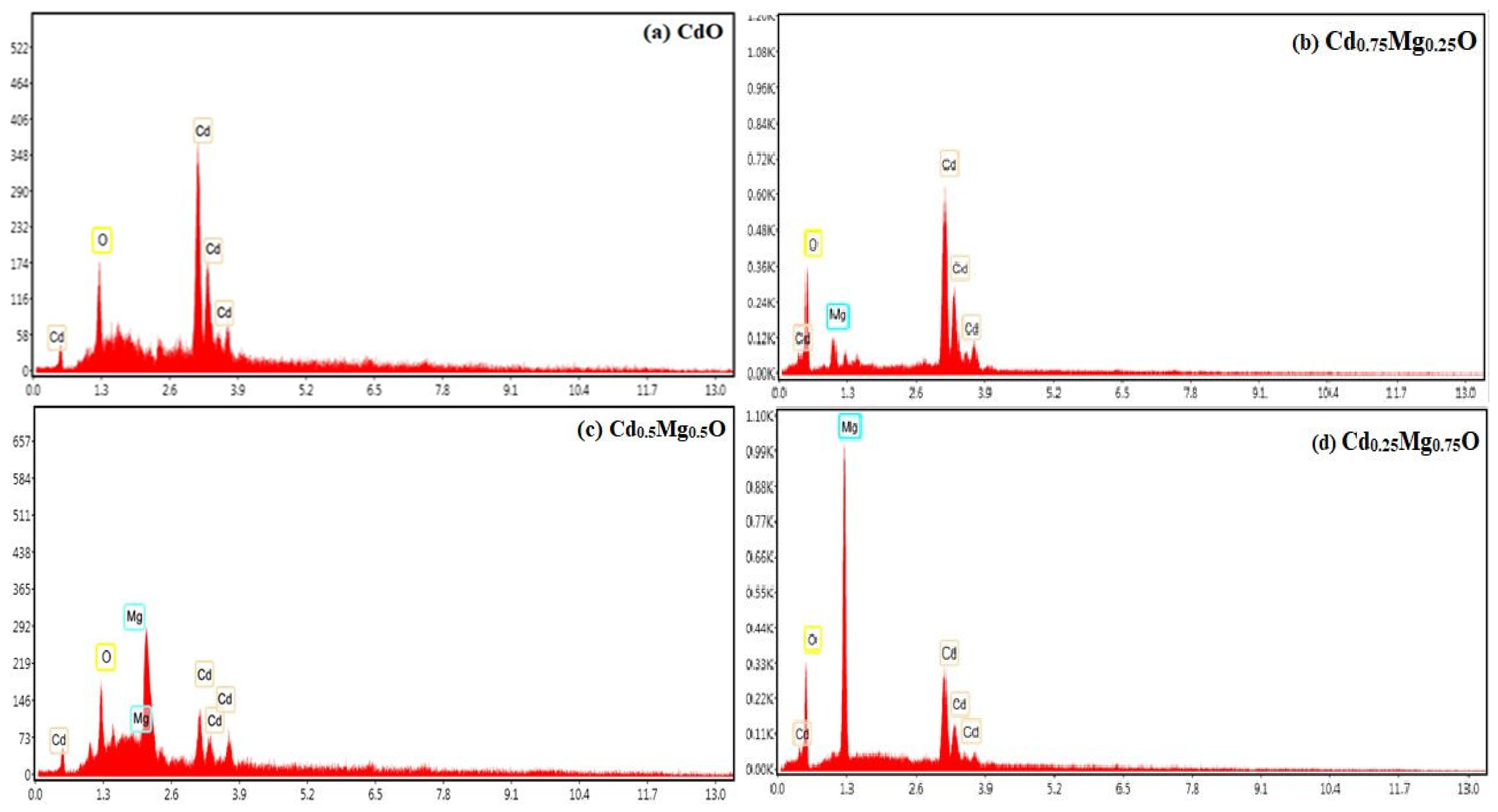
| Element | Atom % (CdO) | Atom % (Cd0.75Mg0.25O) | Atom % (Cd0.5Mg0.5O) | Atom % (Cd0.25Mg0.75O) | Atom % (MgO) |
|---|---|---|---|---|---|
| Cadmium | 52.60 | 39.70 | 26.91 | 13.31 | - |
| Magnesium | - | 12.10 | 25.21 | 37.18 | 53.80 |
| Oxygen | 47.40 | 48.20 | 47.88 | 49.51 | 46.20 |
| Total | 100 | 100 | 100 | 100 | 100 |
Publisher’s Note: MDPI stays neutral with regard to jurisdictional claims in published maps and institutional affiliations. |
© 2021 by the authors. Licensee MDPI, Basel, Switzerland. This article is an open access article distributed under the terms and conditions of the Creative Commons Attribution (CC BY) license (https://creativecommons.org/licenses/by/4.0/).
Share and Cite
Bashir, K.; Mehboob, N.; Ashraf, M.; Zaman, A.; Sultana, F.; Khan, A.F.; Ali, A.; Mushtaq, M.; Uddin, S.; Althubeiti, K. Growth and Investigation of Annealing Effects on Ternary Cd1−xMgxO Nanocomposit Thin Films. Materials 2021, 14, 4538. https://doi.org/10.3390/ma14164538
Bashir K, Mehboob N, Ashraf M, Zaman A, Sultana F, Khan AF, Ali A, Mushtaq M, Uddin S, Althubeiti K. Growth and Investigation of Annealing Effects on Ternary Cd1−xMgxO Nanocomposit Thin Films. Materials. 2021; 14(16):4538. https://doi.org/10.3390/ma14164538
Chicago/Turabian StyleBashir, Khalid, Nasir Mehboob, Muhammad Ashraf, Abid Zaman, Fozia Sultana, Abdul Faheem Khan, Asad Ali, Muhammad Mushtaq, Sarir Uddin, and Khaled Althubeiti. 2021. "Growth and Investigation of Annealing Effects on Ternary Cd1−xMgxO Nanocomposit Thin Films" Materials 14, no. 16: 4538. https://doi.org/10.3390/ma14164538
APA StyleBashir, K., Mehboob, N., Ashraf, M., Zaman, A., Sultana, F., Khan, A. F., Ali, A., Mushtaq, M., Uddin, S., & Althubeiti, K. (2021). Growth and Investigation of Annealing Effects on Ternary Cd1−xMgxO Nanocomposit Thin Films. Materials, 14(16), 4538. https://doi.org/10.3390/ma14164538