Article

Reduction of Hysteresis in Hybrid Perovskite Transistors by Solvent-Controlled Growth

Department of Information Display, College of Sciences, Kyung Hee University, Seoul 02447, Korea
*
Author to whom correspondence should be addressed.
Materials 2021, 14(10), 2573; https://doi.org/10.3390/ma14102573
Submission received: 31 March 2021 / Revised: 7 May 2021 / Accepted: 13 May 2021 / Published: 15 May 2021

Abstract

:
The effect of crystallization process speed on the morphology of solution-processed methyl ammonium lead iodide (MAPbI3) thin films is investigated. Crystallization speed is controlled by varying the number of annealing steps, temperature, and resting time between steps. The resting period allows solvent-controlled growth (SCG) in which crystallization progresses slowly via an intermediate phase—during which solvents slowly evaporate away from the films. SCG results in fewer residues, fewer pinholes, and larger grain sizes. Consequently, thin-film transistors with SCG MAPbI3 exhibit smaller hysteresis in their current-voltage characteristics than those without, demonstrating the benefits of SCG toward hysteresis-free perovskite devices.

1. Introduction

Organic–inorganic hybrid perovskites such as methylammonium lead iodide (CH3NH3PbI3 or MAPbI3) have recently emerged as promising candidates for high-performance and low-cost optoelectronic devices [1,2]. In solar cells, these materials have excelled as light harvesters, reaching record power conversion efficiencies of over 20% in their early stages of development [3]. Such tremendous potential is mainly due to their unique properties, which include tunable bandgaps, high photoluminescence quantum yields, high absorption coefficients, and low density of electronic states, despite low-temperature (<150 °C) processing [2,4,5,6,7]. Besides photovoltaics, organic–inorganic hybrid perovskites are also appealing for other optoelectronic devices, and research on photodetectors [8], thin-film transistors (TFTs) [9], and light-emitting diodes (LEDs) [10] has already made rapid progress.
However, instability in the performance of these devices, especially the hysteresis in their current-voltage (I-V) characteristics, still limits their application in commercial products [8,9,10,11,12,13,14,15,16,17,18,19]. This hysteresis has been linked to ferroelectricity or defect-mediated drift-diffusion of ions in the perovskite thin films during device operation [15,16,17,18,19]. In field-effect devices such as TFTs, the migration of these ions results in a partial screening of the applied gate field, yielding reduced gate modulation of electronic charges [17,18,19,20,21]. Similarly, ion migration also leads to a significant screening of the applied electric field in solar cells and LEDs, leading to measurement speed, time, or history-dependent hysteresis in their I-V characteristics [13,16,18].
The morphology of the perovskite thin films plays a crucial role in the stability of the devices. In particular, the defect-mediated drift-diffusion of ions occurs via grain boundary defects [22,23]. As the perovskite thin films are formed by low temperature solution processes, the formation of polycrystalline films with grain boundaries is unavoidable [22,23]. Structural disorder at the grain boundaries results in defect states such as dangling bonds, elemental vacancies, voids, and pinholes. Besides hysteresis, these defects also have the potential to degrade carrier transport properties of the perovskite thin films, especially the carrier mobility.
Many researchers have attempted to eliminate or counteract the hysteresis via solvent engineering [24,25,26], insertion of self-assembled monolayers (SAMs) [16], suppression of interfacial ferroelectricity [18], doping [19], defect passivation [20], additives [24,25,26,27,28,29], ambient air processing [26,27,28], and so forth [30,31,32]. However, despite all these efforts, the current situation is still far from the complete annihilation of the hysteresis problem.
In this study, we investigate the effects of crystallization process speed on the morphology of the hybrid perovskite methyl ammonium lead iodide (MAPbI3) and its impact on hysteresis in the electrical characteristics of ambient-air-processed MAPbI3 thin-film transistors (TFTs). As crystallization speed can be varied by controlling the speed at which solvents evaporate after spin coating, we vary the annealing temperature, the number of annealing steps, and the interval between steps to achieve various crystallization speeds. We show that adding resting intervals between steps enables solvent-controlled growth (SCG) where crystallization progresses via an intermediate phase during which solvents slowly evaporate away from the films. As a result, SCG decreases the total number of defects and grain boundaries in MAPbI3—thereby significantly reducing hysteresis in MAPbI3 TFTs. This work demonstrates a simple strategy to obtain hysteresis-free perovskite devices in ambient air.

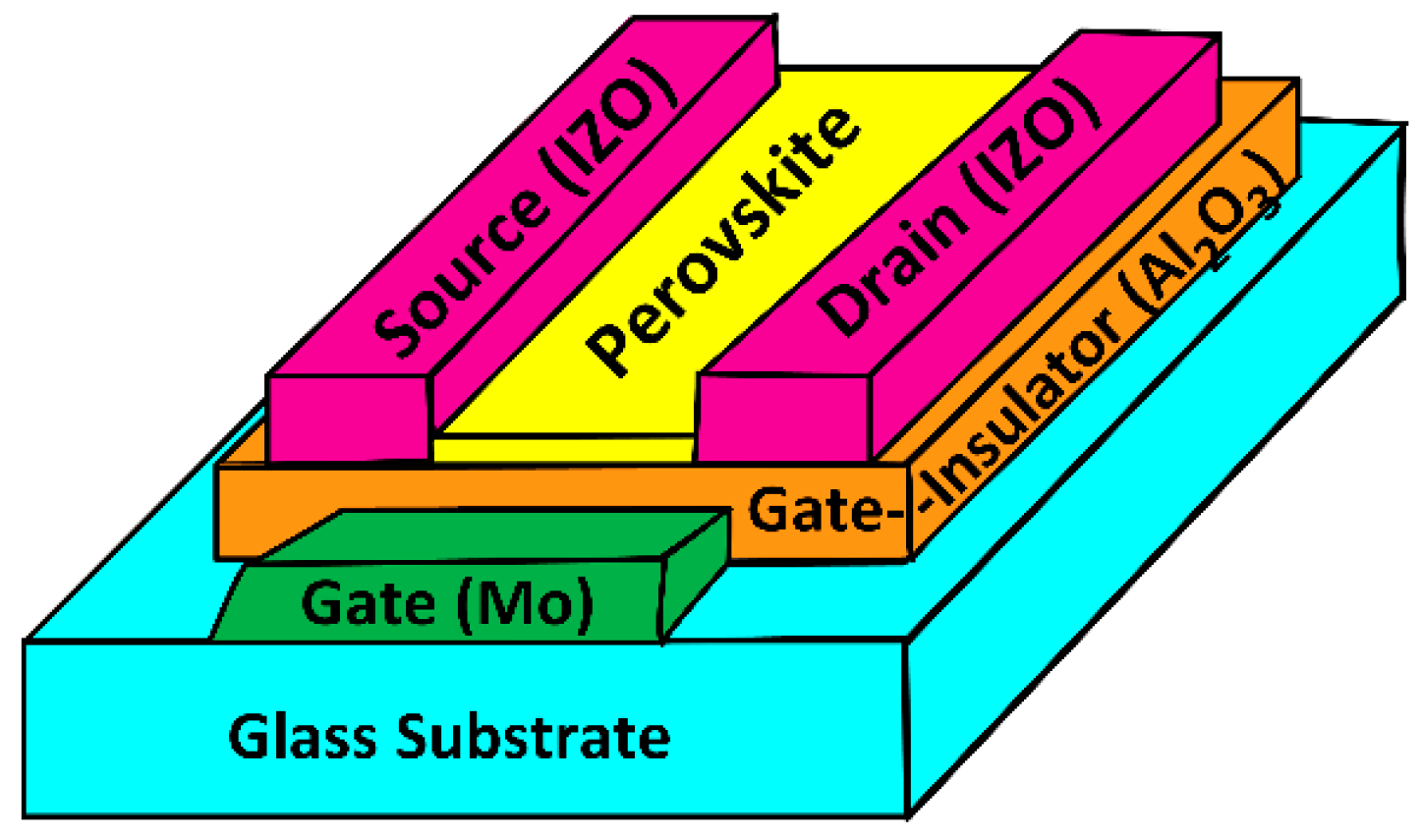
2. Materials and Methods

Using the Laurell WS-400B spin coater (Laurell, North Wales, UK), we spin-coated several MAPbI3 films on bare glass substrates at room temperature in ambient air (relative humidity of 50 ± 5% and temperature of 25 ± 2 °C). For process simplicity and for better ambient air stability, the MAPbI3 films were deposited in ambient air as described previously in [24]. We obtained the precursor solution by dissolving powdered MAI (99.999%, Greatcell Solar, Queanbeyan, Australia) and PbI2 (99%, Merck Korea Ltd./Sigma-Aldrich Korea Ltd., Incheon, Korea) (MAI:PbI2 = 1:1) in a mixed solvent composed of gamma-butyrolactone (GBL) (99%, Merck Korea Ltd./Sigma-Aldrich Korea Ltd., Incheon, Korea) and dimethyl sulfoxide (DMSO) (99.9%, Merck Korea Ltd./Sigma-Aldrich Korea Ltd., Incheon, Korea), followed by stirring for 12 h at 100 °C in ambient air. Spin-coating speed and time were 6000 rotations per minute (rpm) and 70 s, respectively. These conditions yielded approximately 200-nm-thick MAPbI3 films.
To control the crystallization speed, we annealed the films on a hot plate in ambient air at temperatures ranging from 70 to 160 °C. We also varied the number of annealing steps from 1 to 5 and analyzed film morphology by X-ray diffraction (XRD) (Malvern Panalytical Ltd., X’Pert PRO, Royston, UK), X-ray photoelectron spectroscopy (XPS) (ULVAC-PHI, INCORPORATED, PHI 5000 VersaProbe, Kanagawa, Japan), scanning electron microscopy (SEM) (Hitachi High Technologies, S-4700, Tokyo, Japan), and atomic force microscopy (AFM) (Park Systems, XE-100, Suwon, Korea). To minimize the influence of the temperature ramping in the plate heating, we pre-heated the hot plate to the desired temperature before placing the samples on it.
To investigate the hysteresis in I-V characteristics, we fabricated MAPbI3 TFTs with the inverted coplanar structure (Figure 1). The gate electrode was a 40-nm-thick Mo layer deposited by sputtering at 280 °C. The TFTs employed 40-nm Al2O3 thin films as a gate insulator (G.I.) and 60-nm indium zinc oxides (IZO) (280 °C by sputtering) as source (S) and drain (D) electrodes. The capacitance of the Al2O3 layer per unit area (Cox) was estimated to be approximately 200 nF/cm2. We prepared the Al2O3 solution by mixing aluminum chloride (AlCl3) (Merck Korea Ltd./Sigma-Aldrich Korea Ltd. Incheon, Korea), acetonitrile (35%) (Merck Korea Ltd./Sigma-Aldrich Korea Ltd. Incheon, Korea), and ethyleneglycol (65%) (0.2 M) (Merck Korea Ltd./Sigma-Aldrich Korea Ltd. Incheon, Korea). The solution was spin-coated at 2000 rpm for 30 s followed by curing at 250 °C for five minutes (performed to evaporate the solvent) and 5 min UV (NOVASCAN PSD-series, from Novascan Tech Inc., Boone, NC, USA) ozone treatment (wavelengths of 185 and 254 nm, generated by a mercury vapor lamp). During treatment, the 185 nm UV light decomposed atmospheric oxygen molecules (O2) to oxygen-free radicals (·O), which effectively performed oxidative treatments on the surface of the Al2O3. The O can react with O2 to form ozone (O3), which decomposes back to ·O and O2 due to the presence of the 254 nm UV light [33,34,35]. These reactive ·O radicals are highly effective at removing organic residuals from metal oxide film surfaces, increasing the metal-oxygen bonds, and reducing oxygen-related defects. UV treatment thus results in a smooth surface morphology with less defects [33,34,35].
For film densification, we performed a final anneal for 2 h at 350 °C. We defined the source and drain electrodes by patterning a 60-nm-thick IZO layer deposited at 280 °C via sputtering. To avoid pattering, we spin-coated a positive photoresist (PR) (Sigma-Aldrich, Inc., Steinheim, Germany) layer on top of the source and drain electrodes and patterned it to form “banks” into which we spin-coated the MAPbI3. Several TFTs samples were fabricated using MAPbI3 films grown under different conditions.
We retrieved field-effect mobility (µFE) and subthreshold voltage, respectively, from the slope and intercept of the linear regression line of the |ID|1/2 (VDS) plot in the saturation regime (VDS > VGS-VTH). VGS, VDS, and ID, denote the gate voltage, drain voltage, and drain current, respectively. We took the subthreshold swing (SS) as the minimum of (d log (ID)/d VGS)−1 and the hysteresis voltage (VHYS) as the difference between VGS values corresponding to ID equal to 1 nA in the forward and reverse sweeps.

3. Results and Discussion

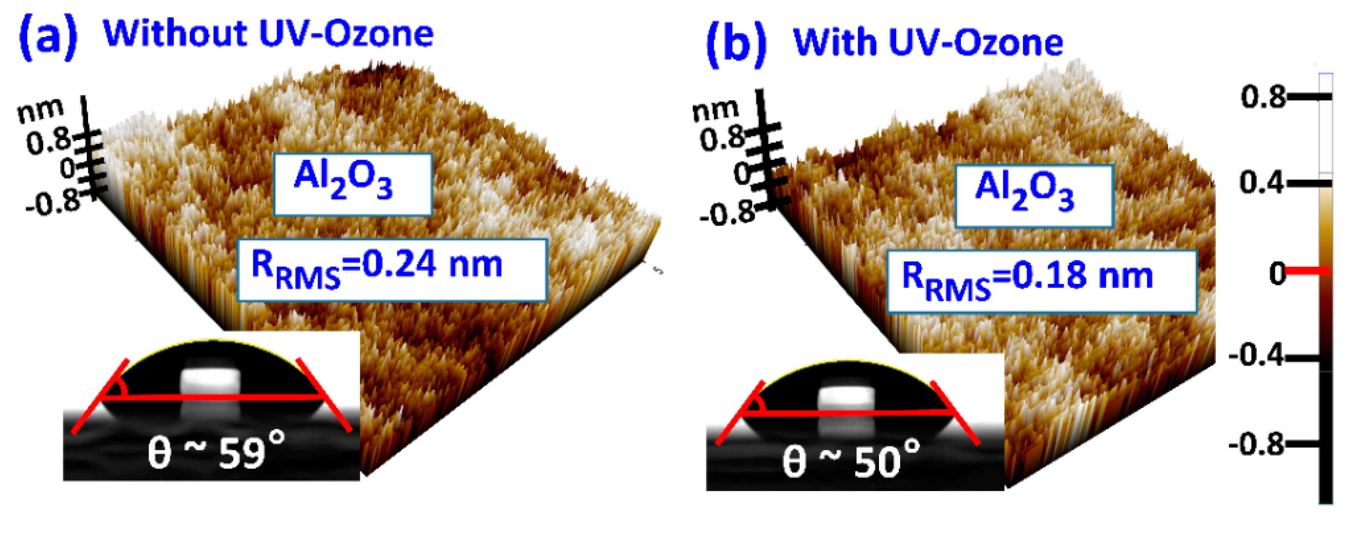
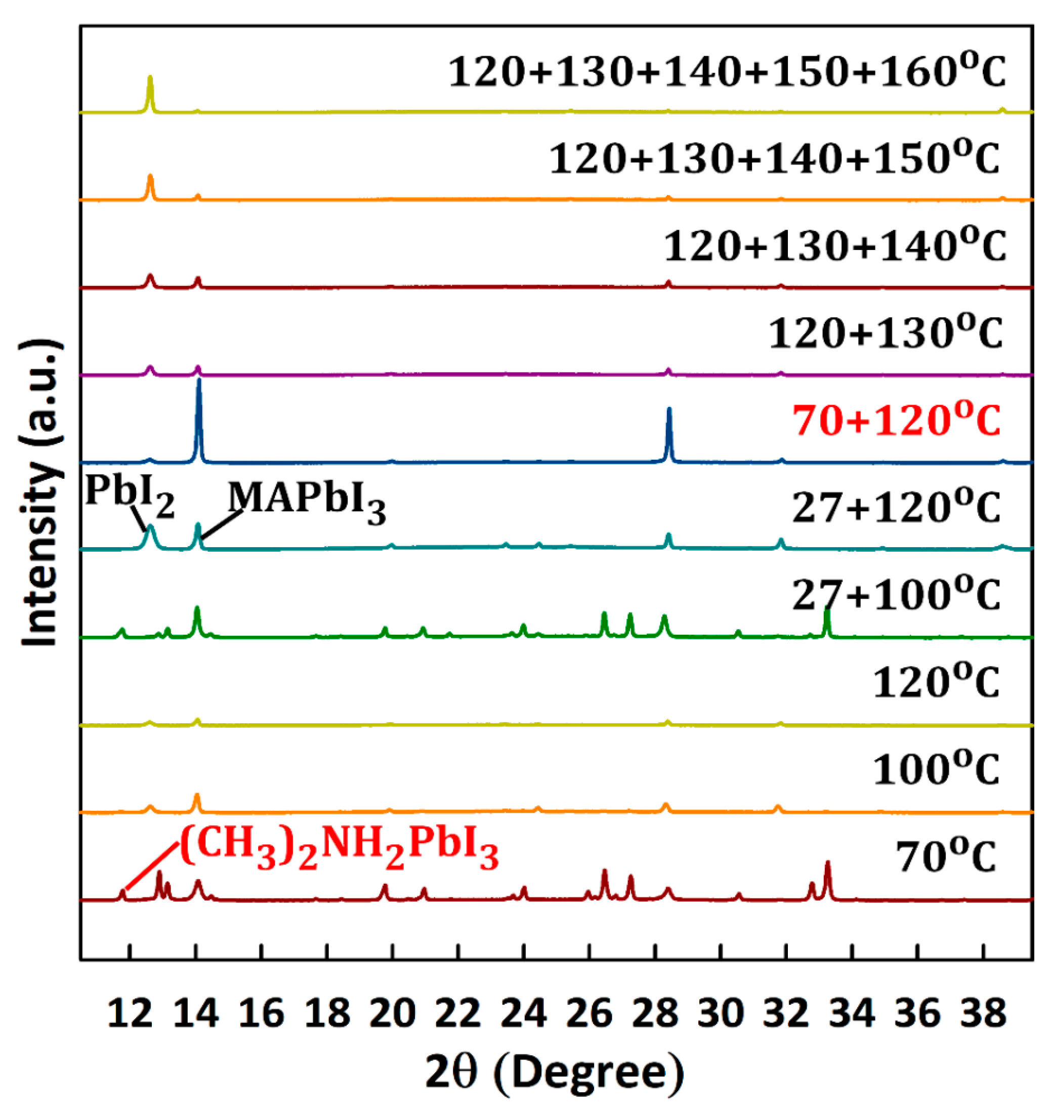
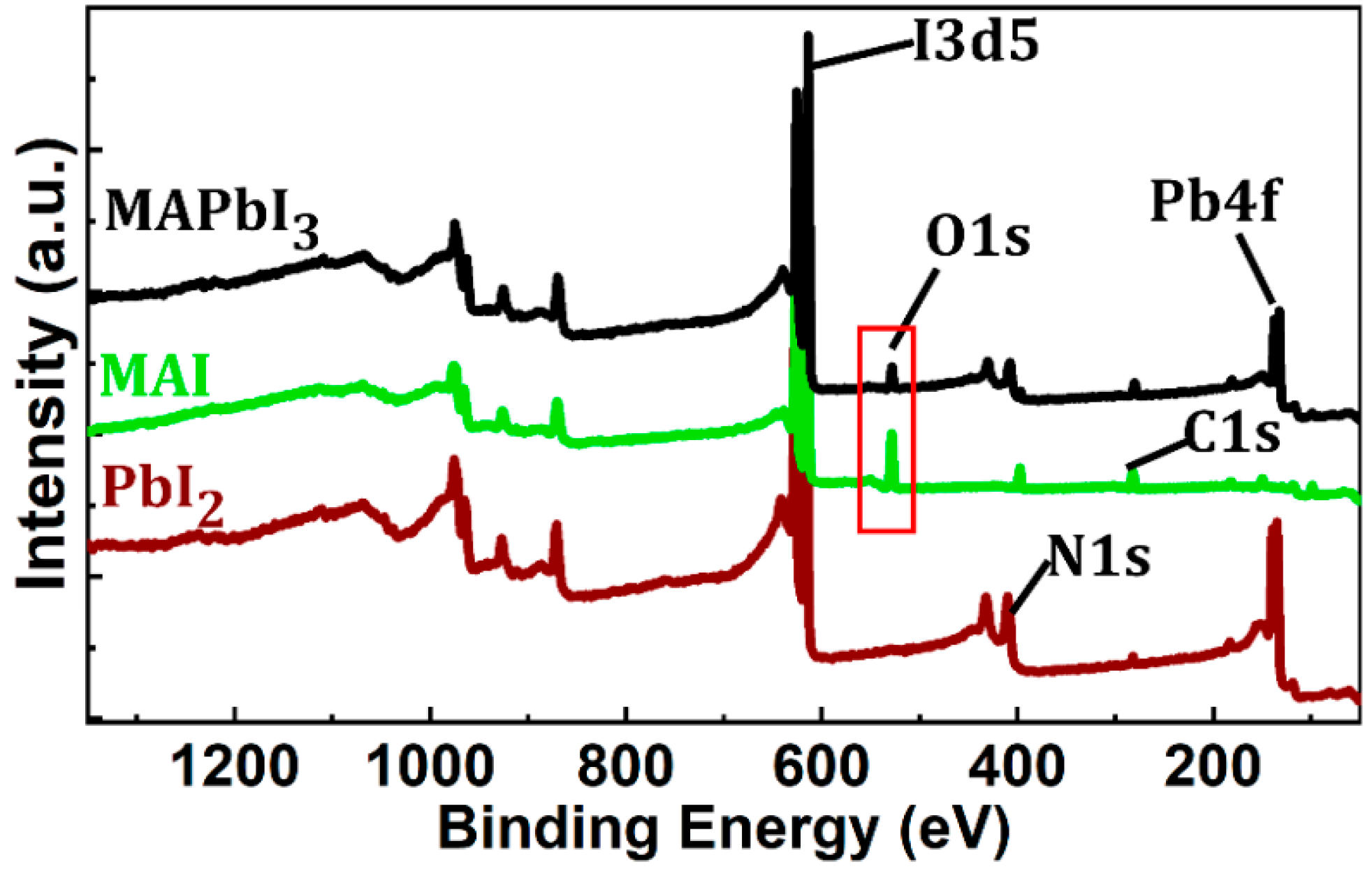
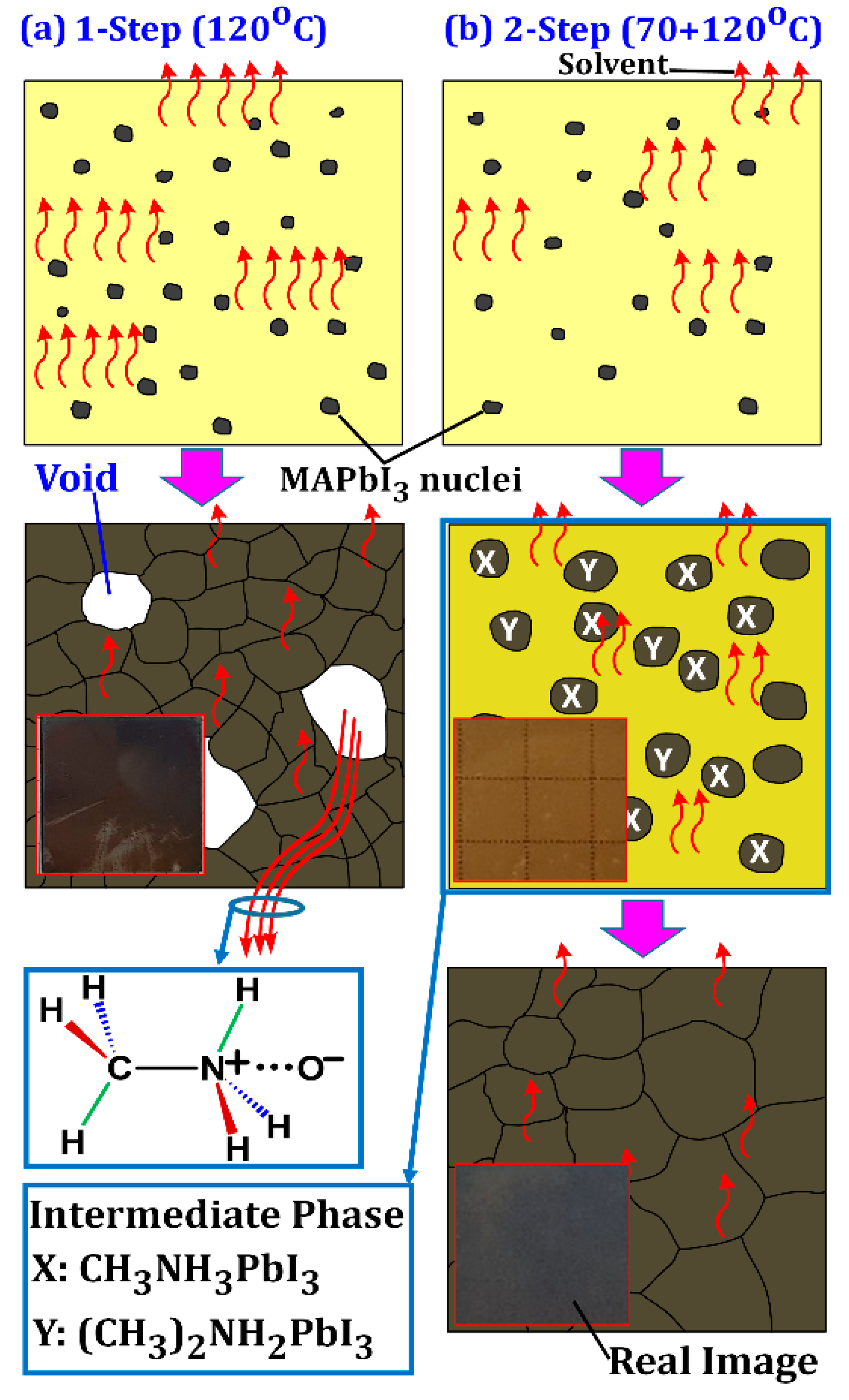
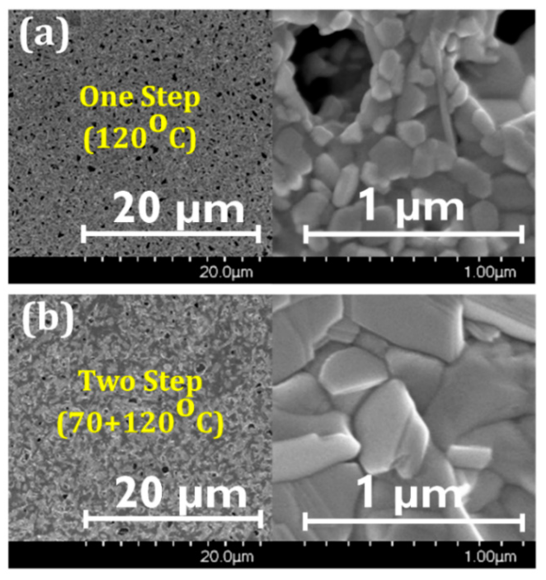
3.1. Film Morphology

For better adhesion, we treated the surface of the Al2O3 with UV-ozone for 10 min before MAPbI3 deposition (Figure 2). Surface properties of Al2O3 films with and without UV-ozone treatment were analyzed using atomic force microscopy (AFM) and contact angle (CA) measurements. Removal of organic solvent residues by the UV-ozone treatment decreases surface roughness as root mean square roughness (RRMS) decreased from 0.24 nm to 0.18 nm. This also improves the wettability of the Al2O3 film.
The contact angle of the Al2O3 G.I. decreased from 59° to 50° after UV-ozone treatment (AHTECH LTS., Gyeonggi-do, Korea), indicating higher surface energy (Figure 2). We calculated the surface energy (γs) of the Al2O3 film before and after UV-ozone treatment using the equation γs = (γw/4) × (1 + cosθ)2 where θ is the contact angle at equilibrium and γw is the water surface free energy and obtained the values 23.96 and 30.60 mJ/m2, respectively. Higher surface energy indicates better interfacial qualities between the MAPbI3 semiconductor and the Al2O3 G.I. It is important to note that without UV-ozone treatment the low wettability of the substrate results in fewer nucleation sites. Although fewer nucleation sites can lead to slightly larger grain sizes, the films without UV-ozone treatment cannot achieve functioning TFTs because they contain a large number of voids and pinholes, which deter lateral conduction in the thin films [36].
Figure 3 shows the XRD patterns of MAPbI3 films fabricated via one-step and multistep annealing processes. A “+” sign indicates a multistep process in the order of appearance. For instance, 70 + 120 °C stands for a two-step annealing process involving an initial annealing at 70 °C followed by second annealing at 120 °C. Each annealing step lasted for 10 min and the multistep annealing processes involved a 1-h resting time (at room temperature in a vacuum) between steps.
Compared to that of films annealed at 70, 100, or 120 °C, the ratio of the MAPbI3 peak-to-PbI2 peak of the film successively annealed at 70 and 120 °C (70 + 120 °C) was the highest, indicating the superiority of multistep to one-step annealing processes. The MAPbI3 peak-to-PbI2 peak ratio dramatically decreased at temperatures >120 °C for both one-step and multistep annealing processes. It is important to note that multistep processes with a maximum temperature of ≤120 °C (e.g., 70 + 100 + 120 °C) yielded similar results to the 70 + 120 °C process. Additionally, resting time ≥ 1 h resulted in similar results (not shown here). As we deposited the MAPbI3 in ambient air, oxygen in the air also strongly influenced the crystal quality. Previous studies have shown the presence of oxygen during annealing to reduce defects without affecting the surface morphology [37,38]. Moreover, it is suggested that oxygen reduces grain boundary defects, yielding better grain-to-grain connection, which is essential for good lateral conduction [24]. The presence of oxygen in the films (Figure 4) was consistent with defect passivation during ambient air processing [21,24,25,38,39] and evaporation of MA via oxygen bonding at temperatures greater than 120 °C (Figure 3).
The 70 + 120 °C annealing process was superior due to the existence of solvent-controlled growth (SCG), which occurred during the resting period. For SCG to occur, crystal seeds are essential, and their formation requires thermal energy [40]. Experimentally, we found temperatures around 70 °C to be sufficient for the seed formation. Given the high boiling points of GBL and DMSO (204 and 189 °C, respectively) [24], high-temperature annealing is required after SCG to effectively complete crystallization. This temperature should be around 120 °C, according to Figure 3. As multistep processes with a maximum temperature of ≤120 °C yielded similar results, we chose the two-step annealing process (70 + 120 °C) for TFT fabrication to keep the process simple.
Figure 5a,b depicts crystallization process mechanisms during one-step and two-step annealing processes, which respectively represent fast and slow crystallization. In the case of the one-step annealing at 120 °C the color of the thin films turned blackish immediately after placing them on the hotplate (see real image in Figure 5a). This indicates rapid growth of MAPbI3 poly crystals with a bandgap of ≅1.72 eV. As air bubbles can be easily trapped during processing in ambient air, rapid solvent evaporation may result in pinhole formation. Additionally, excessive thermal energy may result in MA evaporating with the solvents or via oxygen bonding (Figure 4), leading to void formation in the film (Figure 5a). Extension of the annealing time or additional annealing steps at higher temperatures only results in additional evaporation of MA, leaving behind PbI2. MA is prone to evaporation due to its low boiling point and low sticking properties.
In the case of the two-step annealing process, crystallization progresses slowly via an intermediate state (Figure 5b). The XRD pattern of the 70 °C film shows that this intermediate phase was composed of both MAPbI3 (CH3NH3PbI3) and methyl ammine lead iodide (CH3)2NH2PbI3 crystals (Figure 3). During the intermediate phase, the film was very transparent, so much so that the cutting board under it was clearly visible (grid lines in real image), which further suggests the incomplete formation of MAPbI3. When the samples were left to rest for the duration of 1 h or longer after the 70 °C annealing, crystallization progressed slowly as solvents slowly evaporated from the film. Upon annealing at 120 °C after the resting period, (CH3)2NH2PbI3 disappeared and only the MAPbI3 peak appeared strong, indicating complete crystallization (Figure 3, 70 + 120 °C).
SEM images of the one-step and two-step annealed films confirmed this mechanism. The film annealed at 120 °C contained many voids and/or pinholes as a consequence of the rapid growth (Figure 6a). Fewer voids existed in the 70 + 120 °C film (Figure 6b) as most of the solvents slowly evaporated during the resting period, thereby minimizing the rapid loss of precursors during the second 120 °C annealing step. Furthermore, rapid crystallization from numerous crystal seeds led to smaller grain size in the 120 °C film than 70 + 120 °C film. If the films are left to rest after spin-coating without providing sufficient heat energy through annealing at 70 °C, the intermediate phase will not occur (compare 120 °C and 27 + 120 °C films in Figure 3). Therefore, the first step of annealing at 70 °C is necessary to provide sufficient energy for the crystal seed formation.
Similar results were observed for the inorganic perovskite CsPbI3 where a δ-phase CsPbI3 was observed upon resting the precursor films in a nitrogen-filled glovebox for several tens of minutes [41]. The formation of this additional phase resulted in films becoming more continuous and having a reduced number of pinholes and larger gain size. Additionally, solar cells employing the CsPbI3 films obtained by SCG displayed higher efficiency and could tolerate above 500 h of continuous light soaking [41].
In addition to the crystallization speed, thermal stress also plays a role in the morphology of perovskite films. Perovskite films can accumulate residual stress during processing. Initially, the precursor solution moves freely without any constraint during the spin-coating process due to its low viscosity and lack of interaction with the substrate. However, when the solvent evaporates during the annealing process, conversion into the crystalline perovskite structure enhances chemical interactions with the substrate. The film is thus constrained from expanding or contracting freely, leading to film stress. This constraint is large when the thermal expansion coefficient (CTE) of the film is larger than that of the substrate [42]. This is the case for halide perovskites that have a CTE (approximately 50 × 10−6 K−1) that is five times larger than that of glass (approximately 10 × 10−6 K−1) [43,44]. When the samples were cooled to room temperature after annealing, the perovskite film was constrained from contraction by the underlying glass substrate, resulting in tensile stress building up in the perovskite film. Note that the layer immediately below the perovskite was a 40-nm-thick Al2O3 layer, which was much thinner than the glass (approximately 0.6 mm). The stress was thus determined largely by the glass.
Rolston et al. found the residual stress to have a linear relationship with the temperature at which the film is annealed with higher annealing temperatures resulting in larger stress values [42]. They attributed the correlation between the residual stress and annealing temperature largely to the CTE mismatch between the film and substrate and calculated the predicted stress, σΔT, by
σ Δ T = E p 1 v p ( α s α p ) Δ
where Ep is the perovskite modulus, νp is Poisson’s ratio of the perovskite, αs and αp are the respective thermal expansions of the substrate and perovskite, and ΔT is the temperature gradient when cooling. Using an Ep of approximately 12.5 GPa and νp = 0.3 [42], σΔT is approximately 31 and 65 MPa, respectively, for annealing at 70 and 120 °C. Therefore, the one-step annealing process (120 °C) resulted in initial residual film stress that was much larger than that of the two-step annealing process (70 + 120 °C). Although the two-step annealed sample also underwent annealing at 120 °C, the stress was expected to be less due to the presence of the intermediate phase. Residual film stress can have a significant effect on the optoelectronic properties of the perovskite films and contribute to heat, light, and moisture-based chemical degradation as well as fractures in the device [45,46].

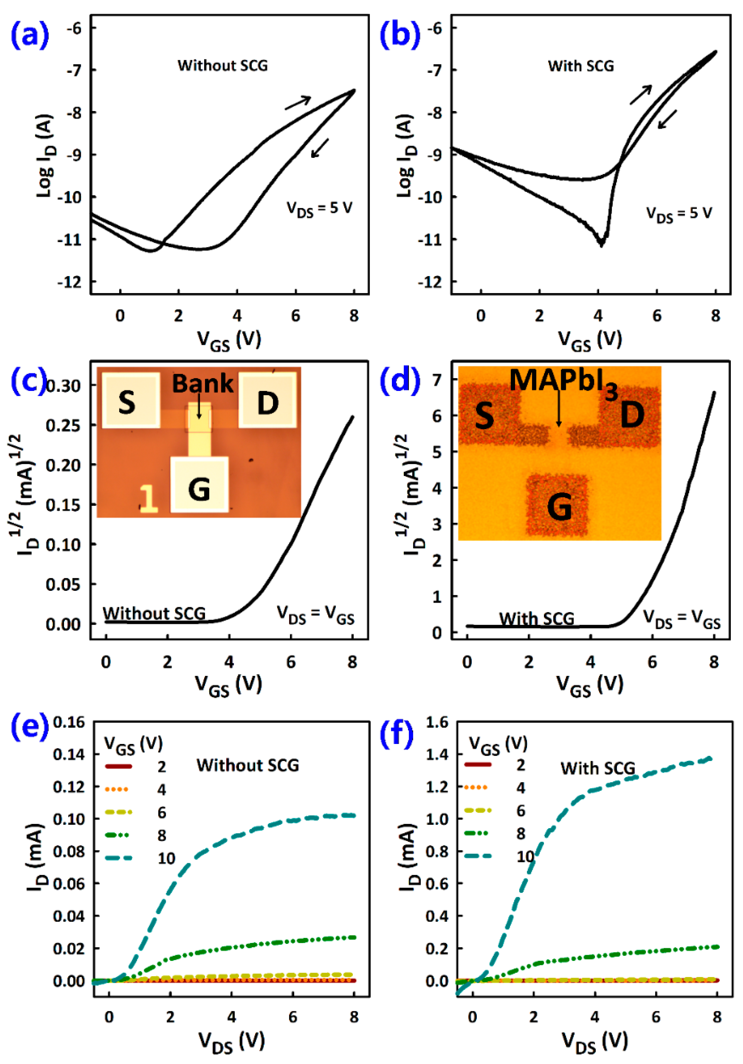
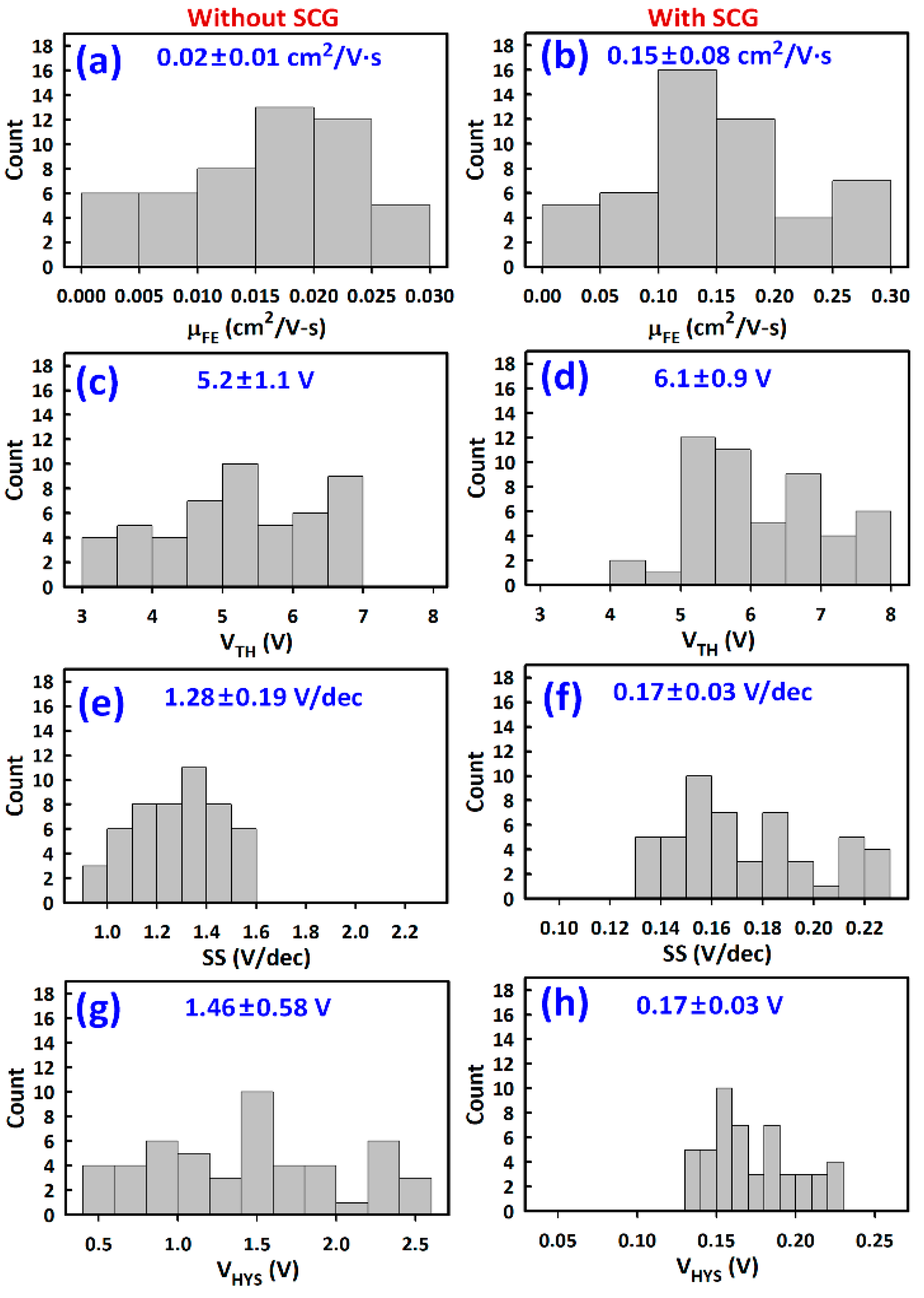
3.2. TFT Current-Voltage Characteristics

Transfer, diode (saturation), and output characteristics of the TFTs were measured as shown in Figure 7. It is interesting to see that hysteresis in the transfer characteristics was smaller in TFTs with SCG MAPbI3 than those without (Figure 7a,b). Hysteresis is due to vacancy-mediated migration of ions in the MAPbI3 [15,16,17]. Given that most of these vacancies occur in grain boundaries or around voids, reduction of hysteresis is consistent with the larger grain size and fewer voids in the SCG-based MAPbI3.
Hysteresis can also originate from ferroelectric effects, trapping at the G.I./MAPbI3 interface, or ion migration inside the G.I. Given that the two sets of TFTs were fabricated with an identical G.I. process, the difference in their hysteresis characteristics is mainly due to changes in the MAPbI3 and not the aforementioned. I, CH3NH3+, and Pb2+ are the three ions in MAPbI3, and the activation energy for vacancy-mediated migration is the lowest for I (0.1–0.6, 0.46–0.84, and >2 eV, respectively) [47,48,49]. I was thus believed to dominate ion drift-diffusion in MAPbI3. Reduced hysteresis in SCG MAPbI3 TFTs was thus consistent with reduced drift-diffusion of I due to the effective reduction in the total number of defects and grain boundaries. These results were consistent with a previous report on lead-free layered perovskite transistors where grain boundary passivation and grain size enlargement were found to reduce hysteresis and increase TFT reproducibility and reliability [50].
The diode characteristics measured by shorting the gate and drain electrodes showed a steeper slope for TFTs with SCG than those without (Figure 7c,d). The steeper slope is an indication of higher µFE as shown in Figure 8. The output characteristics also showed about an order of magnitude higher current in TFTs with SCG than those without, consistent with better film morphology for TFTs with SCG (Figure 7e,f). The current crowding at low VDS values was also more pronounced in the TFTs without SCG than those with SCG, indicating higher resistance at source/drain contacts of the former—possibly due to the presence of many voids.
Owing to the good film morphology achieved by SCG, the µFE improved from 0.02 ± 0.01 to 0.15 ± 0.08 cm2/V·s (Figure 8a,b). The VTH values were 6.1 ± 0.9 and 5.2 ± 1.1 V, respectively, for TFTs with and without SCG (Figure 8c,d). The slightly lower VTH in TFTs without SCG could be related to a slightly different surface potential due to defects or mobile ions. There were evidently more defect states in the TFTs without SCG than those with SCG, given that SS of the former (1.28 ± 0.19 V/dec) was approximately ten times larger than that of the latter (0.17 ± 0.03 V/dec) (Figure 8e,f). The total trap density (NT) can be calculated from NT = {SS(log(e))/(kBT/q) − 1}(Cox/q) where kB, T, and q are respectively the elementary electric charge, Boltzmann’s constant, and temperature in kelvins [51]. NT values of the TFTs with and without SCG were approximately 1.29 × 10¹² and 1.06 × 1013 cm2·V−1, respectively [51,52]. The difference in NT was mainly due to the bulk states, given that the TFTs employ the same gate insulator.
Positive gate bias stress (PBS) stability of the MAPbI3 TFTs was also investigated. The PBS was achieved by applying a constant VGS of 10 V to the TFTs while grounding the source and drain electrodes for 3600 s. The PBS was interrupted at different points to measure the transfer characteristics as shown in Figure 9.
Consistent with having fewer defects, the TFTs with SCG showed better PBS stability compared to those without. PBS results in trapping of carriers at the semiconductor/gate-insulator interface. These trapped carriers screened the gate field, resulting in the reduction of the effective applied VGS, which led to positive the turn-on voltage shift (ΔVON). However, the shifting of the VON of the MAPbI3 TFTs investigated herein was bidirectional, consistent with the contribution of other forms of hysteresis, particularly due to ion migration. The fluctuation of the VTH, especially at the early stages of the PBS, was much larger for the TFT without SCG—underscoring the importance of defect reduction by SCG. The similar ΔVON after 3600 s can be explained by the fact that the TFTs employed the same gate insulator.
The VHSY decreased from 1.46 ± 0.58 to 0.17 ± 0.03 V after SCG (Figure 8g,h). Overall, SCG also resulted in less variation in the extracted parameters, indicating better film uniformity. However, even after SCG, the hysteresis was still quite significant, especially in the off-state characteristics (Figure 7b). Additionally, there is still room to optimize the thermal treatment employed herein and further improvement can be achieved by employing additional strategies to suppress the formation of vacancies and ion migration such as the incorporation of multi cation mixtures and Lewis base acid treatments [53,54,55]. Additionally, various surface treatments such as the insertion of SAMs [16] and the use of additives to passivate surface defects [24,25,26,27,28,29] can be applied to further mitigate the difference in the surface energy or roughness between the G.I. and the perovskite semiconductor to achieve smoother pinhole-free thin films.

4. Conclusions

The effect of crystallization process speed on the morphology of MAPbI3 thin films processed from a solution in ambient air was investigated. The crystallization speed can be controlled by varying the number of annealing steps, temperature, and resting time between steps. The resting period allows solvent-controlled growth (SCG) in which crystallization progresses slowly via an intermediate phase during which solvents slowly evaporate away from the films. SCG decreases the total number of defects and grain boundaries in MAPbI3—thereby significantly reducing hysteresis in MAPbI3 TFTs.
To achieve SCG, a two-step annealing process is required. It is recommended to do the first step at approximately 70 °C followed by resting for at least one hour before the second step at approximately 120 °C. Adding steps between the 70 and 120 °C annealing or increasing the resting time does not significantly yield better results. Annealing at temperatures larger than 120 °C degrades the films due to the evaporation of MAI whereas annealing at temperatures lower than 70 °C is not sufficient for crystallization. A one-step annealing at 120 °C results in rapid crystallization from numerous crystal seeds, which leads to smaller grain size and voids in the film. This work demonstrates a simple strategy to obtain hysteresis-free perovskite devices in ambient air and thus opens up the scope of using organic–inorganic hybrid perovskites for applications beyond optoelectronic devices.

Author Contributions

Methodology, M.M.; investigation, F.H.; data curation, R.N.B.; writing—original draft preparation, M.M.; writing—review and editing, M.M.; supervision, M.M. All authors have read and agreed to the published version of the manuscript.

Funding

This work was funded in part by the National Research Foundation of South Korea (NRF) through the Korean Government Ministry of Science, ICP and Future Planning (MSIP) under Grant NRF-2019R1F1A1059601.

Institutional Review Board Statement

Not applicable.

Informed Consent Statement

Not applicable.

Data Availability Statement

Data sharing is not applicable to this article.

Acknowledgments

We would like to thank Jin Jang for his support in fabricating the devices and Jehwang Ryu and Amar Gupta for their support in taking the SEM images.

Conflicts of Interest

The authors declare no conflict of interest. The funders had no role in the design of the study; in the collection, analyses, or interpretation of data; in the writing of the manuscript; or in the decision to publish the results.

References

  1. Krishnamurthy, S.; Pandey, P.; Kaur, J.; Chakraborty, S.; Nayak, P.K.; Sadhanala, A.; Ogale1, S. Organic–inorganic hybrid and inorganic halide perovskites: Structural and chemical engineering, interfaces, and optoelectronic properties. J. Phys. D Appl. Phys. 2021, 54, 133002. [Google Scholar] [CrossRef]
  2. Chen, Q.; De Marco, N.; Yang, Y.M.; Song, T.B.; Chen, C.C.; Zhao, H.; Yang, Y. Under the spotlight: The organic–inorganic hybrid halide perovskite for optoelectronic applications. Nano Today 2015, 10, 355–396. [Google Scholar] [CrossRef] [Green Version]
  3. Green, M.; Dunlop, E.; Hohl-Ebinger, J.; Yoshita, M.; Kopidakis, N.; Hao, X. Solar cell efficiency tables (version 57). Prog. Photovolt. Res. 2021, 29, 3–15. [Google Scholar] [CrossRef]
  4. Stranks, S.D.; Snaith, H.J. Metal-halide perovskites for photovoltaic and light-emitting devices. Nat. Nanotechnol. 2015, 10, 391–402. [Google Scholar] [CrossRef] [PubMed]
  5. Sadhanala, A.; Deschler, F.; Thomas, T.H.; Dutton, S.E.; Goedel, K.C.; Hanusch, F.C.; Lai, M.L.; Steiner, U.; Bein, T.; Docampo, P.; et al. Preparation of single-phase films of CH3NH3Pb(I1–xBrx)3 with sharp optical band edges. J. Phys. Chem. Lett. 2014, 5, 2501–2505. [Google Scholar] [CrossRef]
  6. Shi, D.; Adinolfi, V.; Comin, R.; Yuan, M.; Alarousu, E.; Buin, A.; Chen, Y.; Hoogland, S.; Rothenberger, A.; Katsiev, K.; et al. Low trap-state density and long carrier diffusion in organolead trihalide perovskite single crystals. Science 2015, 347, 519–522. [Google Scholar] [CrossRef] [Green Version]
  7. Sadhanala, A.; Ahmad, S.; Zhao, B.; Giesbrecht, N.; Pearce, P.M.; Deschler, F.; Hoye, R.L.Z.; Gödel, K.C.; Bein, T.; Docampo, P.; et al. Blue-green color tunable solution processable organolead chloride–bromide mixed halide perovskites for optoelectronic applications. Nano Lett. 2015, 15, 6095–6101. [Google Scholar] [CrossRef] [Green Version]
  8. Miaoa, J.; Zhang, F. Recent progress on highly sensitive perovskite photodetectors. J. Mater. Chem. C 2019, 7, 1741–1791. [Google Scholar] [CrossRef]
  9. Wu, T.; Pisula, W.; Rashid, M.Y.A.; Gao, P. Application of Perovskite-Structured Materials in Field-Effect Transistors. Adv. Electron. Mater. 2019, 5, 1900444. [Google Scholar] [CrossRef]
  10. Liu, X.K.; Xu, W.; Bai, S.; Jin, Y.; Wang, J.; Friend, R.H.; Gao, F. Metal halide perovskites for light-emitting diodes. Nat. Mater. 2021, 20, 10–21. [Google Scholar] [CrossRef]
  11. Dualeh, A.; Moehi, T.; Tetreault, N.; Teuscher, J.; Gao, P.; Nazeeruddin, M.K.; Gratzel, M. Temperature dependence of transport properties of spiro-MeOTAD as a hole transport material in solid-state dye-sensitized solar cells. ACS Nano 2013, 7, 2292–2301. [Google Scholar] [CrossRef]
  12. Snaith, H.J.; Abate, A.; Ball, J.M.; Eperon, G.E.; Leijtens, T.; Noel, N.K.; Stranks, S.D.; Wang, J.T.-W. Wojciechowski, K., Zhang, W. Anomalous hysteresis in perovskite solar cell. J. Phys. Chem. Lett. 2014, 5, 1511–1515. [Google Scholar] [CrossRef] [PubMed]
  13. Nayak, P.K.; Mahesh, S.; Snaith, H.J.; Cahen, D. Photovoltaic solar cell technologies: Analysing the state of the art. Nat. Rev. Mater. 2019, 4, 269–285. [Google Scholar] [CrossRef]
  14. Zhao, B.; Bai, S.; Kim, V.; Lamboll, R.; Shivanna, R.; Auras, F.; Richter, J.M.; Yang, L.; Dai, L.; Alsari, M.; et al. High-efficiency perovskite–polymer bulk heterostructure light-emitting diodes. Nat. Photonics 2018, 12, 783–789. [Google Scholar] [CrossRef]
  15. Seol, D.; Jeong, A.; Han, M.; Seo, S.; Yoo, T.; Choi, W.; Jung, H.; Shin, H.; Kim, Y. Origin of hysteresis in CH3NH3PbI3 perovskite thin films. Adv. Funct. Mat. 2017, 27, 1701924. [Google Scholar] [CrossRef]
  16. Tumen-Ulzii, G.; Matsushima, T.; Klotz, D.; Leyden, M.R.; Wang, P.; Qin, C.; Lee, J.; Lee, S.; Yang, Y.; Adachi, C. Hysteresis-less and stable perovskite solar cells with a self-assembled monolayer. Commun. Mater. 2020, 1, 31. [Google Scholar] [CrossRef]
  17. Shao, Y.; Fang, Y.; Li, T.; Wang, Q.; Dong, Q.; Deng, Y.; Yuan, Y.; Wei, H.; Wang, M.; Gruverman, A.; et al. Grain boundary dominated ion migration in polycrystalline organic–inorganic halide perovskite films. Energ. Environ. Sci. 2016, 9, 1752–1759. [Google Scholar] [CrossRef]
  18. Ma, W.; Zhang, X.; Xu, Z.; Guo, H.; Lu, G.; Meng, S. Reducing Anomalous Hysteresis in Perovskite Solar Cells by Suppressing the Interfacial Ferroelectric Order. ACS Appl. Mater. Inter. 2020, 12, 12275–12284. [Google Scholar] [CrossRef]
  19. Haque, F.; Hoang, N.T.T.; Ji, J.; Mativenga, M. Effect of Precursor Composition on Ion Migration in Hybrid Perovskite CH3NH3PbI3. IEEE Electron Devices Lett. 2019, 40, 1756–1759. [Google Scholar] [CrossRef]
  20. Kang, D.; Park, N. On the Current–Voltage Hysteresis in Perovskite Solar Cells: Dependence on Perovskite Composition and Methods to Remove Hysteresis. Adv. Mater. 2019, 31, 1805214. [Google Scholar] [CrossRef]
  21. Zhong, Y.; Hufnagel, M.; Thelakkat, M.; Li, C.; Huettner, S. Role of PCBM in the Suppression of Hysteresis in Perovskite Solar Cells. Adv. Funct. Mater. 2020, 30, 1908920. [Google Scholar] [CrossRef] [Green Version]
  22. Zhang, C.; Sun, D. Valy Vardeny, Multifunctional optoelectronic–spintronic device based on hybrid organometal trihalide perovskites. Z. Adv. Electron. Mater. 2017, 3, 1600426. [Google Scholar] [CrossRef]
  23. Zhang, Y.; Liu, M.; Eperon, G.E.; Leijtens, T.C.; McMeekin, D.; Saliba, M.; Zhang, W.; Bastiani, M.; Pertrozza, A.; Herz, L.M.; et al. Charge selective contacts, mobile ions and anomalous hysteresis in organic–inorganic perovskite solar cells. Mater. Horiz. 2015, 2, 315. [Google Scholar] [CrossRef]
  24. Mativenga, M.; Ji, J.; Hoang, N.T.T.; Haque, F. Ambient air stability of hybrid perovskite thin-film transistors by ambient air processing. Adv. Mater. Interfaces 2020, 7, 1901777. [Google Scholar] [CrossRef]
  25. Luo, P.; Xia, W.; Zhou, S.; Sun, L.; Cheng, J.; Xu, C.; Lu, Y. Solvent engineering for ambient-air-processed, phase-stable CsPbI3 in perovskite solar cells. J. Phys. Chem. Lett. 2016, 7, 3603–3608. [Google Scholar] [CrossRef]
  26. Jeon, N.; Noh, J.; Kim, Y.; Yang, W.; Ryu, S.; Seok, S. Solvent engineering for high-performance inorganic–organic hybrid perovskite solar cells. Nat. Mater. 2014, 13, 897–903. [Google Scholar] [CrossRef]
  27. Gong, J.; Guo, P.; Benjamin, S.E.; Van Patten, P.G.; Schaller, R.D.; Xu, T. Cation engineering on lead iodide perovskites for stable and high-performance photovoltaic applications. J. Energy Chem. 2018, 27, 1017–1039. [Google Scholar] [CrossRef]
  28. Yang, C.; Chueh, C.; Liang, P.W.; Crump, M.; Lin, F.; Zhu, Z.; Jen, A.K.Y. Effects of formamidinium and bromide ion substitution in methylammonium lead triiodide toward high-performance perovskite solar cells. Nano Energy 2016, 22, 328–337. [Google Scholar] [CrossRef] [Green Version]
  29. Ji, J.; Haque, F.; Hoang, N.T.T.; Mativenga, M. Ambipolar transport in methylammonium lead iodide thin film transistors. Crystals 2019, 9, 539. [Google Scholar] [CrossRef] [Green Version]
  30. Huang, L.; Hu, Z.; Xu, J.; Zhang, K.; Zhang, J.; Zhu, Y. Multi-step slow annealing perovskite films for high performance planar perovskite solar cells. Sol. Energy Mater. Sol. 2015, 141, 377–382. [Google Scholar] [CrossRef]
  31. Kim, Y.G.; Kim, T.Y.; Oh, J.H.; Choi, K.S.; Kim, Y.J.; Kim, S.Y. Cesium lead iodide solar cells controlled by annealing temperature. Phys. Chem. Chem. Phys. 2017, 19, 6257–6263. [Google Scholar] [CrossRef] [PubMed]
  32. Foley, B.J.; Girard, J.; Sorenson, B.A.; Chen, A.Z.; Niezgoda, J.S.; Alpert, M.R.; Harper, A.F.; Smilgies, D.M.; Clancy, P.; Saidi, W.A.; et al. Controlling nucleation, growth, and orientation of metal halide perovskite thin films with rationally selected additives. J. Mater. Chem. A 2017, 5, 113–123. [Google Scholar] [CrossRef]
  33. Bukke, R.N.; Avis, C.; Chowdhury, M.D.H.; Kim, T.; Lin, T.; Jang, J. Improvement in performance of solution-processed indium-zinc-tin oxide thin-film transistors by UV/O3 treatment on zirconium oxide gate insulator. Jpn. J. Appl. Phys. 2016, 55, 03CC02–03CC08. [Google Scholar]
  34. Mude, N.N.; Bukke, R.N.; Jang, J. High Performance of Solution-Processed Amorphous p-Channel Copper-Tin-Sulphur-Gallium Oxide Thin-Film Transistor by UV/O3 Photocuring. ACS Appl. Mater. Interfaces 2021, 13, 20277–20287. [Google Scholar] [CrossRef]
  35. Oluwabi, A.T.; Gaspar, D.; Katerski, A.; Mere, A.; Krunks, M.; Pereira, L.; Oja Acik, I. Influence of Post-UV/Ozone Treatment of Ultrasonic-Sprayed Zirconium Oxide Dielectric Films for a Low-Temperature Oxide Thin Film Transistor. Materials 2020, 13, 6. [Google Scholar] [CrossRef] [Green Version]
  36. Pylnev, M.; Barbisan, A.M.; Wei, T.-C. Effect of wettability of substrate on metal halide perovskite growth. Appl. Surf. Sci. 2021, 541, 148559. [Google Scholar] [CrossRef]
  37. Jingbi, Y.; Yang, Y.; Hong, Z.; Song, T.-B.; Meng, L.; Liu, Y.; Jiang, C.; Zhou, H.; Chang, W.-H.; Li, G.; et al. Moisture assisted perovskite film growth for high performance solar cells.Y. Appl. Phys. Lett. 2014, 105, 183902. [Google Scholar]
  38. Ren, Z.; Ng, A.; Shen, Q.; Gokkaya, H.C.; Wang, J.; Yang, L.; Yiu, W.; Bai, G.; Djurišić, A.B.; Leung, W.W.; et al. Thermal assisted oxygen annealing for high efficiency planar CH3NH3PbI3 perovskite solar cells. Sci. Rep. 2014, 4, 6752. [Google Scholar] [CrossRef]
  39. Brenes, R.; Guo, D.; Osherov, A.; Noel, N.K.; Eames, C.; Hutter, E.M.; Pathak, S.K.; Niroui, F.; Friend, R.H.; SaifulIslam, M.; et al. Metal halide perovskite polycrystalline films exhibiting properties of single crystals. Joule 2017, 1, 155–167. [Google Scholar] [CrossRef] [Green Version]
  40. John, M.; Nima, Y.; Chris, P.; Joop, H.; Jan, S. Nucleation and Crystal Growth in Continuous Crystallization. In The Handbook of Continuous Crystallization; Royal Society of Chemistry: London, UK, 2020. [Google Scholar]
  41. Wang, P.; Zhang, X.; Zhou, Y.; Jiang, Q.; Ye, Q.; Chu, Z.; Li, X.; Yang, X.; Yin, Z.; You, J. Solvent-controlled growth of inorganic perovskite films in dry environment for efficient and stable solar cells. Nat. Commun. 2018, 9, 2225. [Google Scholar] [CrossRef]
  42. Rolston, N.; Bush, K.A.; Printz, A.D.; Gold-Parke, A.; Ding, Y.; Toney, M.F.; McGehee, M.D.; Dauskardt, R.H. Engineering stress in perovskite solar cells to improve stability. Adv. Energy Mater. 2018, 15, 1802139. [Google Scholar] [CrossRef]
  43. Ramirez, C.; Yadavalli, S.K.; Garces, H.F.; Zhou, Y.; Padture, N.P. Thermo-mechanical behavior of organic-inorganic halide perovskites for solar cells. Scr. Mater. 2018, 150, 36–41. [Google Scholar] [CrossRef]
  44. Bansal, N.P.; Doremus, R.H. Handbook of Glass Properties; Elsevier: Amsterdam, The Netherlands, 1986. [Google Scholar]
  45. Osterwald, C.R.; McMahon, T.J. History of accelerated and qualification testing of terrestrial photovoltaic modules: A literature review. Prog. Photovolt. Res. Appl. 2009, 17, 11–33. [Google Scholar] [CrossRef]
  46. McMahon, T.J. Accelerated testing and failure of thin-film PV modules. Prog. Photovolt. Res. Appl. 2004, 12, 235–248. [Google Scholar] [CrossRef]
  47. Yin, W.-J.; Shi, T.; Yan, Y. Unusual defect physics in CH3NH3PbI3 perovskite solar cell absorber. Appl. Phys. Lett. 2014, 104, 063903. [Google Scholar] [CrossRef]
  48. Eames, G.C.; Frost, J.M.; Barnes, P.R.; O’regan, B.C.; Walsh, A.; Islam, M.S. Ionic transport in hybrid lead iodide perovskite solar cells. Nat. Commun. 2015, 6, 7497. [Google Scholar] [CrossRef] [Green Version]
  49. Weller, H.M.T.; Weber, O.J.; Henry, P.F.; Pumpo, A.M.D.; Hansen, T.C. Complete structure and cation orientation in the perovskite photovoltaic methylammonium lead iodide between 100 and 352 K. Chem. Commun. 2015, 51, 4180–4183. [Google Scholar] [CrossRef] [Green Version]
  50. Zhu, H.; Liu, A.; Shim, K.I.; Hong, J.; Han, J.W.; Noh, Y.Y. High-Performance and Reliable Lead-Free Layered-Perovskite Transistors. Adv. Mater. 2020, 32, 2002717. [Google Scholar] [CrossRef]
  51. Su, B.-Y.; Chu, S.-Y.; Juang, Y.-D.; Chen., H.-C. High-performance low-temperature solution-processed InGaZnO thin-film transistors via ultraviolet-ozone photo-annealing. Appl. Phys. Lett. 2013, 102, 192101. [Google Scholar] [CrossRef]
  52. Bukke, R.N.; Saha, J.K.; Mude, N.N.; Kim, Y.G.; Lee, S.; Jang, J. Lanthanum Doping in Zinc Oxide for Highly Reliable Thin-Film Transistors on Flexible Substrates by Spray Pyrolysis. ACS Appl. Mater. Interfaces 2020, 31, 35164–35174. [Google Scholar]
  53. Zhu, X.; Lee, J.; Lu, W.D. Iodine Vacancy Redistricution in Organic Inorganic Halide Perovskite Films and Resistive Switching Effects. Adv. Mater. 2017, 29, 1700527. [Google Scholar] [CrossRef] [PubMed]
  54. Saliba, M.; Matsui, T.; Seo, J.-Y.; Domanski, K.; Correa-Baena, J.-P.; Nazeeruddin, M.K.; Zakeeruddin, S.M.; Tress, W.; Abate, A.; Hagfeldt, A.; et al. Cesium-containing triple cation perovskite solar cells: Improved stability, reproducibility and high efficiency. Energ. Environ. Sci. 2016, 9, 1989. [Google Scholar] [CrossRef] [PubMed] [Green Version]
  55. Nikolka, M.; Schweicher, G.; Armitage, J.; Nasrallah, I.; Jellett, C.; Guo, Z.; Hurhangee, M.; Sadhanala, A.; McCulloch, I.; Nielsen, C.B.; et al. Performance Improvements in Conjugated Polymer Devices by Removal of Water-Induced Traps. Adv. Mater. 2018, 30, 1801874. [Google Scholar] [CrossRef]
Figure 1. Schematic structure of MAPbI3 TFTs.
Materials 14 02573 g001
Figure 2. Atomic force microscopy (AFM) images and contact angles of Al2O3 films; (a) before and (b) after UV-ozone treatment.
Materials 14 02573 g002
Figure 3. X-ray diffraction (XRD) patterns of MAPbI3 films grown via one-step and multistep annealing processes at various temperatures. A “+” sign indicates a multistep process in the order of appearance. For instance, 70 + 120 °C stands for a two-step annealing process involving an initial annealing at 70 °C followed by second annealing at 120 °C. Each annealing step lasted for 10 min and the multistep annealing processes involved a 1-h resting time (at room temperature in a vacuum) between steps.
Materials 14 02573 g003
Figure 4. X-ray photoelectron spectroscopy (XPS) results for the one-step 120 °C annealed film.
Materials 14 02573 g004
Figure 5. Mechanism of crystal formation in MAPbI3 by (a) one-step and (b) two-step annealing processes.
Materials 14 02573 g005
Figure 6. Scanning electron microscopy (SEM) images of MAPbI3 films fabricated with (a) one-step and (b) two-step annealing processes.
Materials 14 02573 g006
Figure 7. Typical current-voltage (I-V) characteristics of MAPbI3 TFTs with one-step (without SCG) and two-step (with SCG) annealed MAPbI3 films. (a,b) Transfer characteristics with forward and reverse sweeps. (c,d) Diode characteristics measured with shorted gate and drain electrodes (i.e., saturation regime). (e,f) Output characteristics. The TFTs had channel width of 100 µm and channel length of 20 µm. Insets of c and d are optical images of a MAPbI3 TFT before and after spin-coating MAPbI3, respectively.
Materials 14 02573 g007
Figure 8. TFT Parameters extracted from 100 devices with and without solvent-controlled growth (SCG). (a,b) Field-effect mobility (µFE). (c,d) Threshold voltage (VTH). (e,f) Subthreshold swing (SS). (g,h) Hysteresis voltage (VHYS). The first and second numbers inside the figures (A ± B) are the mean and standard deviation, respectively.
Materials 14 02573 g008
Figure 9. Positive bias stress (PBS) stability of MAPbI3 TFTs. (a,b) Transfer characteristics of the TFTs at various stages of the stress period. (c,d) Turn-on voltage shift (ΔVON) as a function of stress time. The VON is taken as the VGS at which the ID starts to monotonically increase.
Materials 14 02573 g009
Publisher’s Note: MDPI stays neutral with regard to jurisdictional claims in published maps and institutional affiliations.

