Optical Etching to Pattern Microstructures on Plastics by Vacuum Ultraviolet Light


Abstract
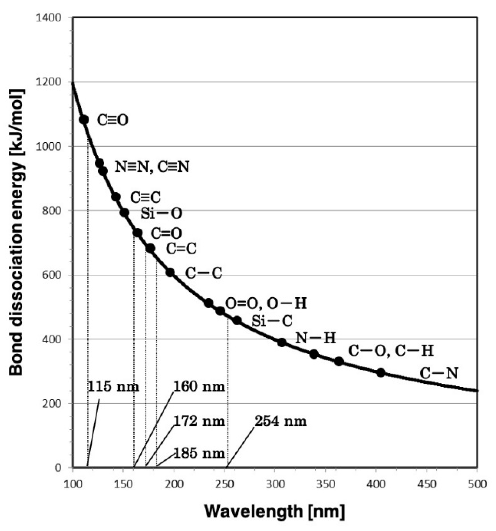
1. Introduction
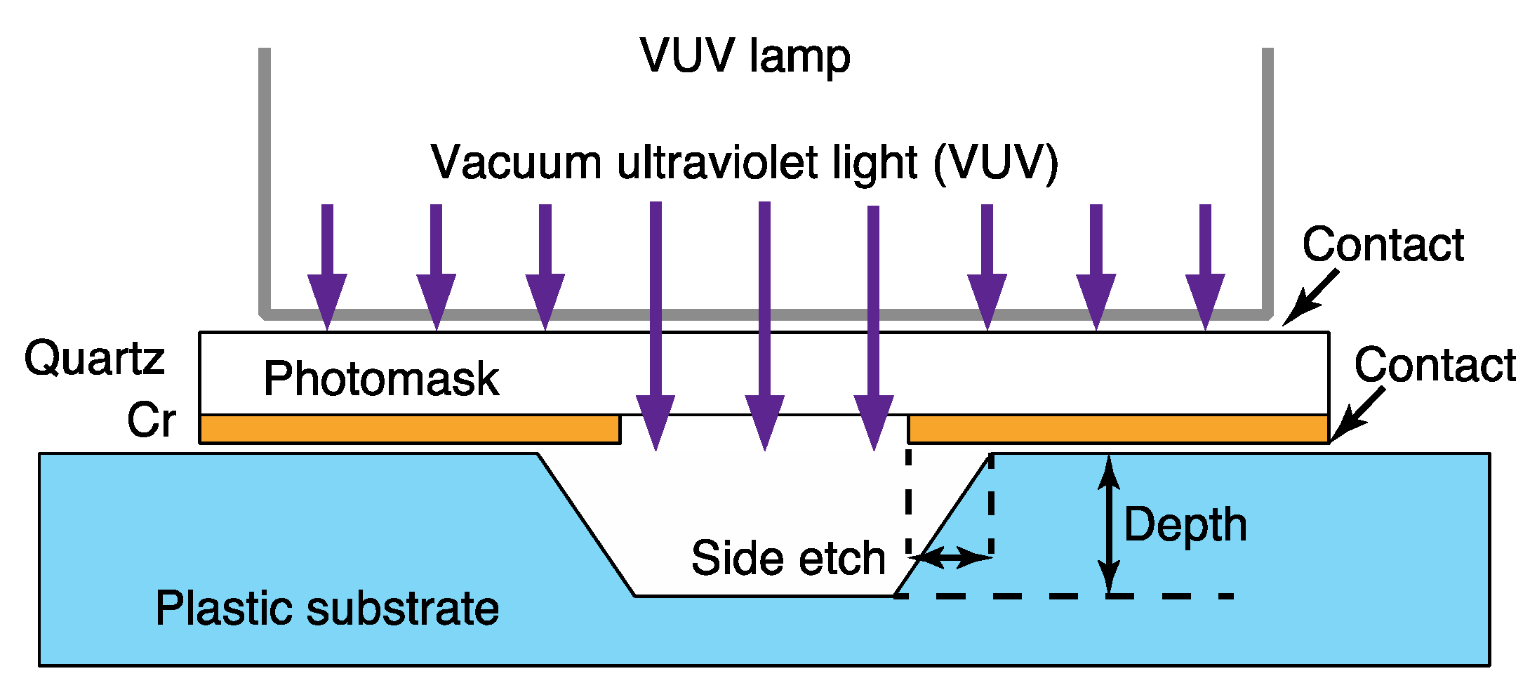
2. Materials and Methods
3. Results
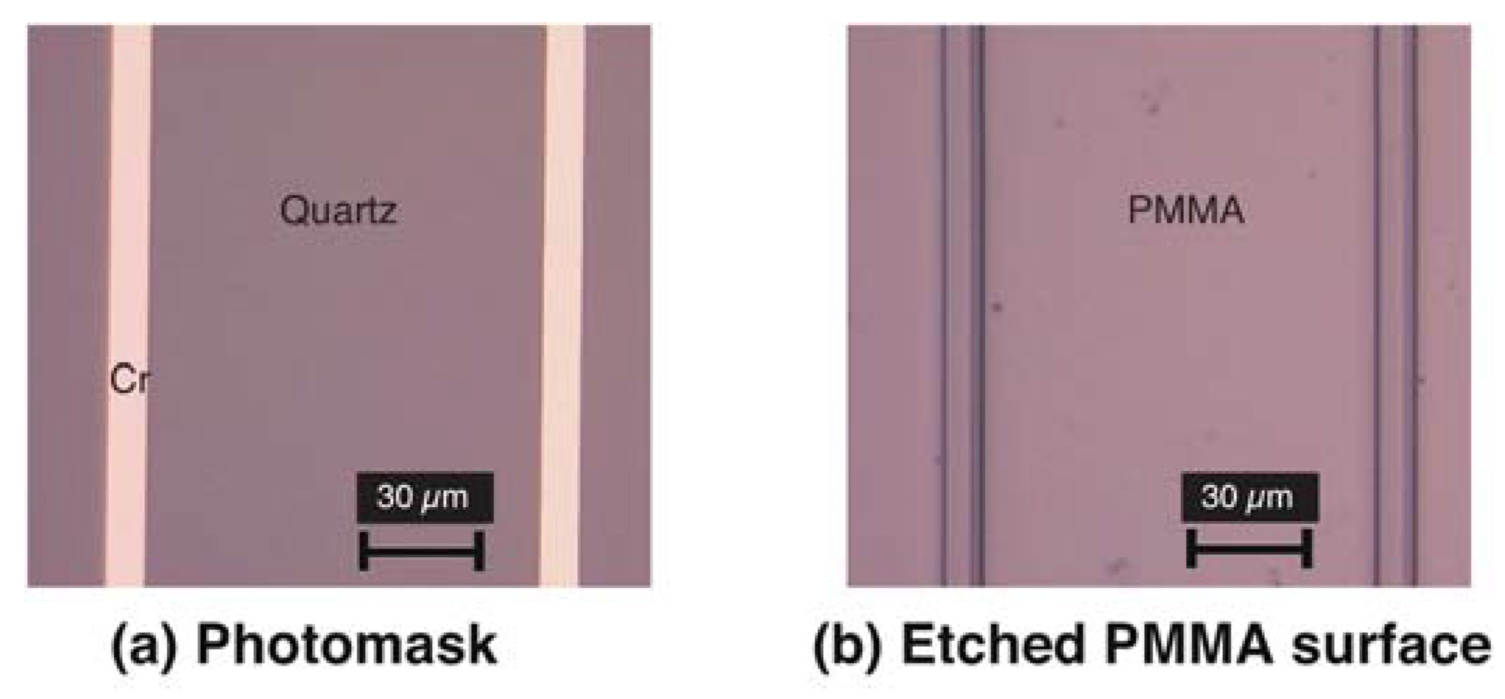
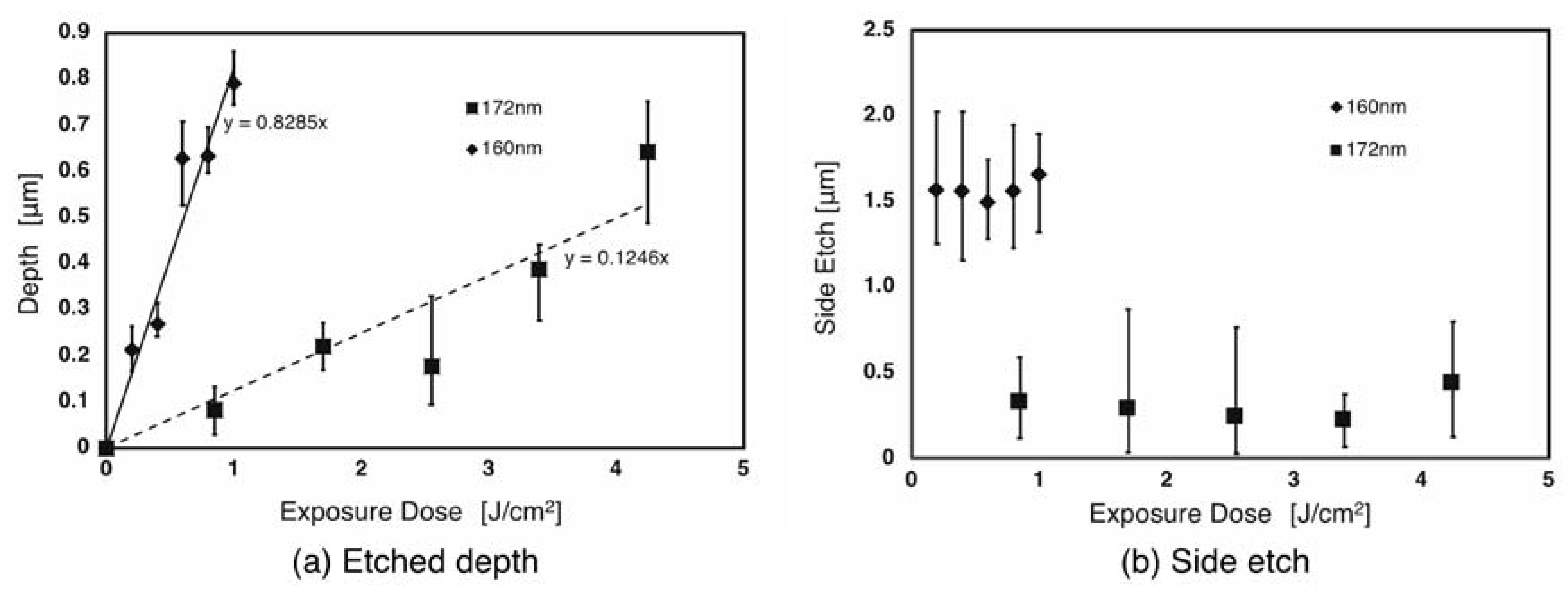
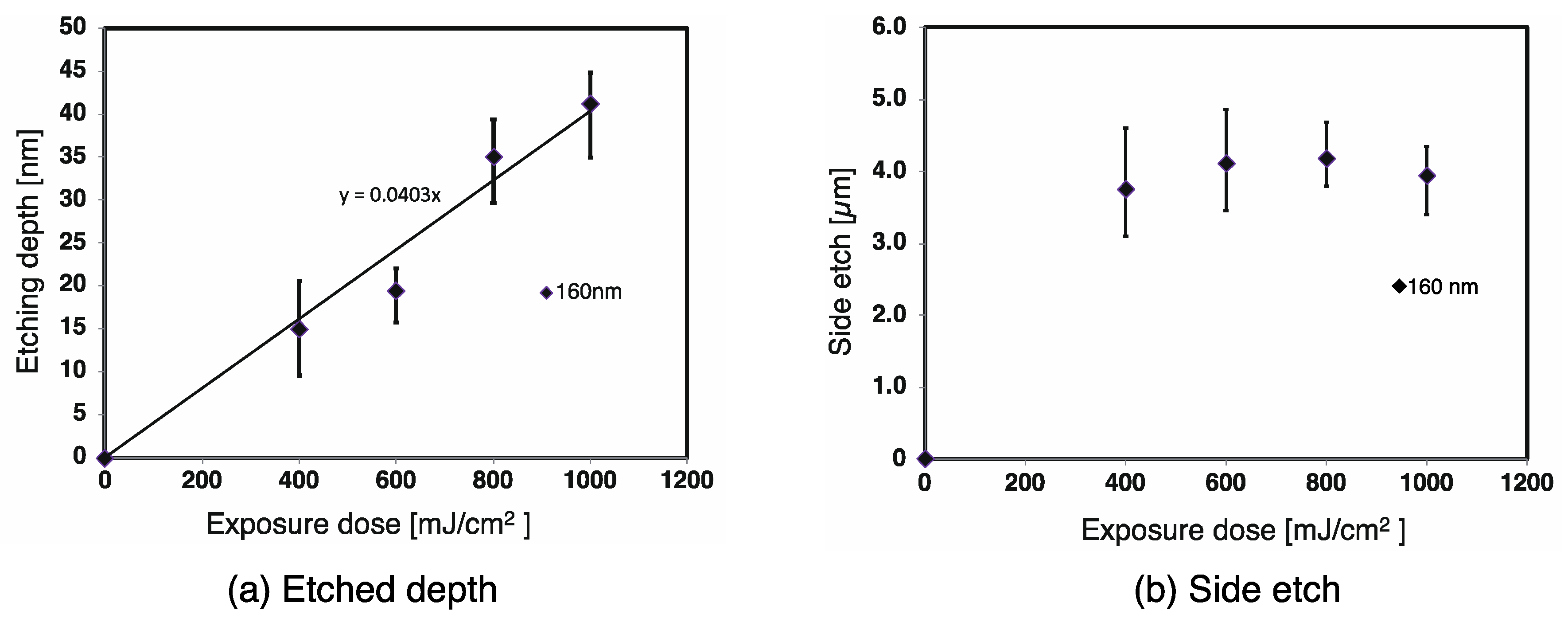
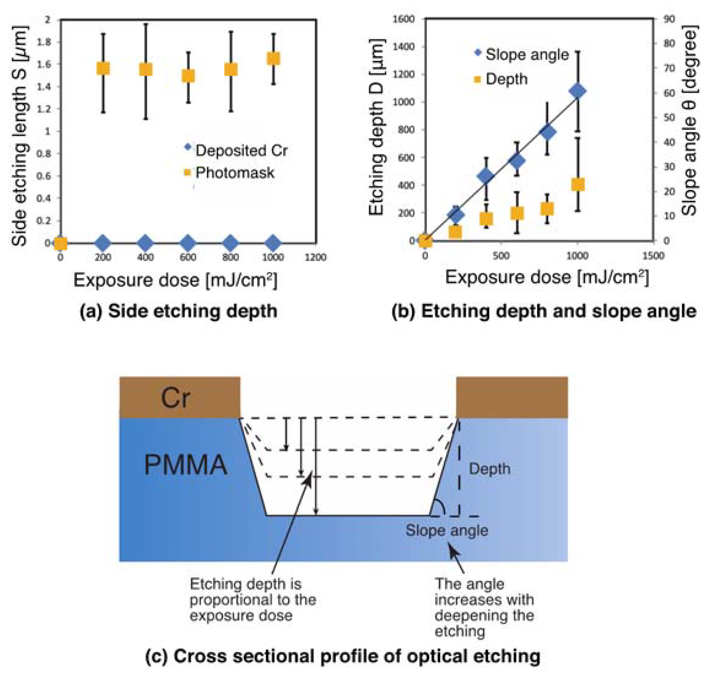
3.1. Optical Etching
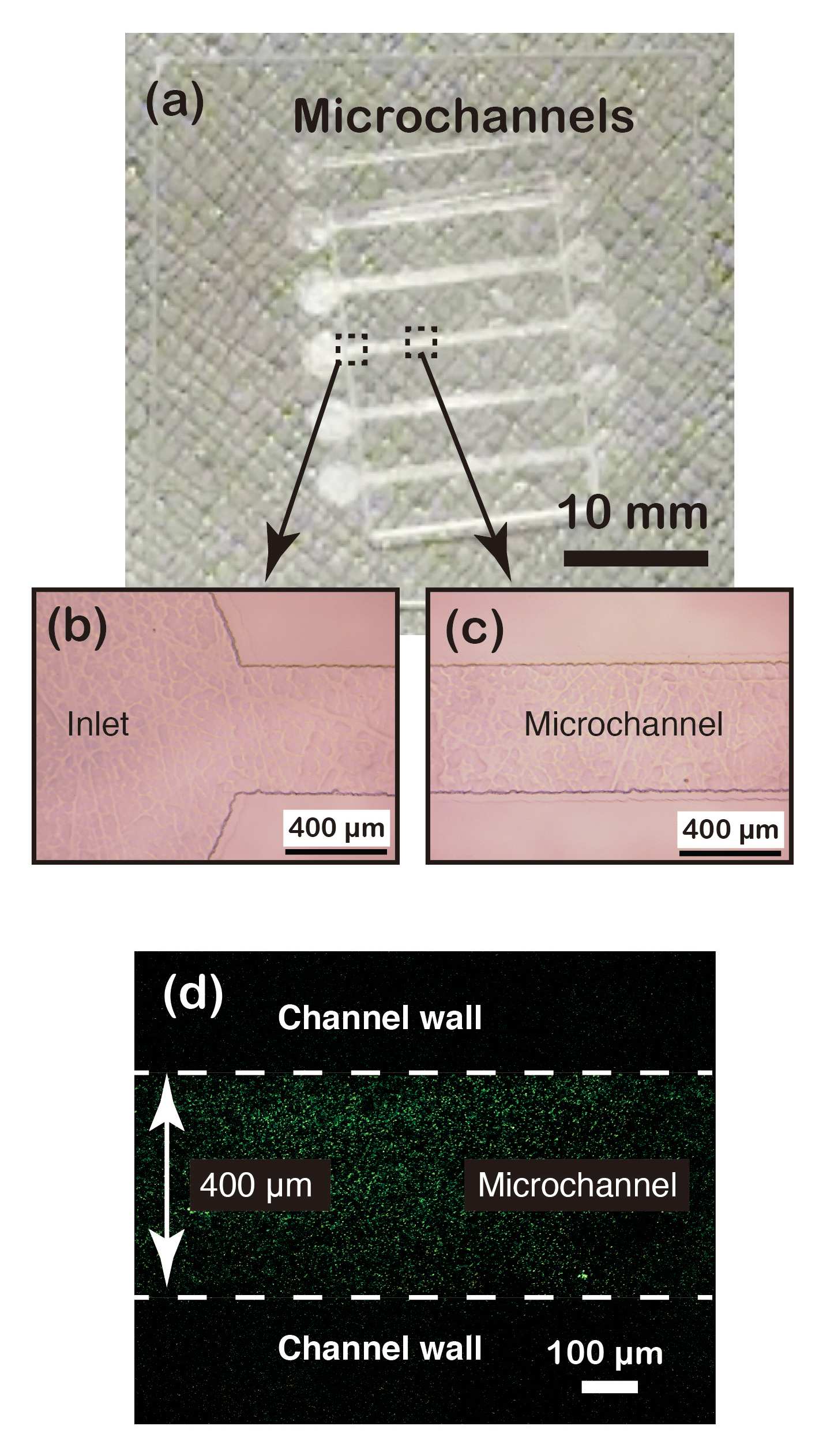
3.2. Fabrication of Microfluidic Device by Optical Etching and Bonding
4. Discussion
5. Conclusions
Author Contributions
Funding
Conflicts of Interest
References
- Chou, W.L.; Lee, P.Y.; Yang, C.L.; Huang, W.Y.; Lin, Y.S. Recent advances in applications of droplet microfluidics. Micromachines 2015, 6, 1249–1271. [Google Scholar] [CrossRef]
- Liu, Z.; Han, X.; Qin, L. Recent progress of microfluidics in translational applications. Adv. Healthc. Mater. 2016, 5, 871–888. [Google Scholar] [CrossRef]
- Gao, D.; Jin, F.; Zhou, M.; Jiang, Y. Recent advances in single cell manipulation and biochemical analysis on microfluidics. Analyst 2019, 144, 766–781. [Google Scholar] [CrossRef] [PubMed]
- Song, Y.; Lin, B.; Tian, T.; Xu, X.; Wang, W.; Ruan, Q.; Guo, J.; Zhu, Z.; Yang, C. Recent progress in microfluidics-based biosensing. Anal. Chem. 2018, 91, 388–404. [Google Scholar] [CrossRef] [PubMed]
- Miled, A.; Greener, J. Recent advancements towards full-system microfluidics. Sensors 2017, 17, 1707. [Google Scholar] [CrossRef] [PubMed]
- Brince, P.K.; Panigrahi, A.K.; Singh, V.; Singh, S.G. Nonlithographic fabrication of plastic-based nanofibers integrated microfluidic biochip for sensitive detection of infectious biomarker. ACS Appl. Mater. Interfaces 2017, 9, 39994–40005. [Google Scholar]
- Chandrasekaran, A.; Kalashnikov, N.; Rayes, R.; Wang, C.; Spicer, J.; Moraes, C. Thermal scribing to prototype plastic microfluidic devices, applied to study the formation of neutrophil extracellular traps. Lab Chip 2017, 17, 2003–2012. [Google Scholar] [CrossRef] [PubMed]
- Klammer, I.; Hofmann, M.C.; Buchenauer, A.; Mokwa, W.; Schnakenberg, U. Long-term stability of PDMS-based microfluidic systems used for biocatalytic reactions. J. Micromech. Microeng. 2006, 16, 2425. [Google Scholar] [CrossRef]
- Adamiak, W.; Kałuża, D.; Jönsson-Niedziolka, M. Compatibility of organic solvents for electrochemical measurements in PDMS-based microfluidic devices. Microfluid. Nanofluid. 2016, 20, 127. [Google Scholar] [CrossRef]
- Guckenberger, D.J.; de Groot, T.E.; Wan, A.M.D.; Beebe, D.J.; Young, E.W.K. Micromilling: A method for ultra-rapid prototyping of plastic microfluidic devices. Lab Chip 2015, 15, 2364–2378. [Google Scholar] [CrossRef]
- Iwai, K.; Shih, K.C.; Lin, X.; Brubaker, T.A.; Sochol, R.D.; Lin, L. Finger-powered microfluidic systems using multilayer soft lithography and injection molding processes. Lab Chip 2014, 14, 3790–3799. [Google Scholar] [CrossRef] [PubMed]
- Mair, D.A.; Geiger, E.; Pisano, A.P.; Fréchet, J.M.J.; Svec, F. Injection molded microfluidic chips featuring integrated interconnects. Lab Chip 2006, 6, 1346–1354. [Google Scholar] [CrossRef] [PubMed]
- Xia, Y.; McClelland, J.J.; Gupta, R.; Qin, D.; Zhao, X.M.; Sohn, L.L.; Celotta, R.J.; Whitesides, G.M. Replica molding using polymeric materials: A practical step toward nanomanufacturing. Adv. Mater. 1997, 9, 147–149. [Google Scholar] [CrossRef]
- Fiorini, G.S.; Jeffries, G.D.M.; Lim, D.S.W.; Kuyper, C.L.; Chiu, D.T. Fabrication of thermoset polyester microfluidic devices and embossing masters using rapid prototyped polydimethylsiloxane molds. Lab Chip 2003, 3, 158–163. [Google Scholar] [CrossRef] [PubMed]
- Chiang, Y.M.; Bachman, M.; Chu, C.; Li, G.P. Characterizing the Process of cast molding microfluidic systems. In Microfluidic Devices and Systems II, Proceedings of the Symposium on Micromachining and Microfabrication, Santa Clara, CA, US, 19 August 1999; International Society for Optics and Photonics: Bellingham, WA, USA, 1999; Volume 3877, pp. 303–311. [Google Scholar]
- Bhattacharjee, N.; Urrios, A.; Kang, S.; Folch, A. The upcoming 3D-printing revolution in microfluidics. Lab Chip 2016, 16, 1720–1742. [Google Scholar] [CrossRef] [PubMed]
- Ho, C.M.B.; Ng, S.H.; Li, K.H.H.; Yoon, Y.J. 3D printed microfluidics for biological applications. Lab Chip 2015, 15, 3627–3637. [Google Scholar] [CrossRef]
- Chen, J.; Zhou, Y.; Wang, D.; He, F.; Rotello, V.M.; Carter, K.R.; Watkins, J.J.; Nugen, S.R. UV-nanoimprint lithography as a tool to develop flexible microfluidic devices for electrochemical detection. Lab Chip 2015, 15, 3086–3094. [Google Scholar] [CrossRef]
- Lin, T.Y.; Do, T.; Kwon, P.; Lillehoj, P.B. 3D printed metal molds for hot embossing plastic microfluidic devices. Lab Chip 2017, 17, 241–247. [Google Scholar] [CrossRef]
- Nilsson, D.; Balslev, S.; Kristensen, A. microfluidic dye laser fabricated by nanoimprint lithography in a highly transparent and chemically resistant cyclo-olefin copolymer (COC). J. Micromech. Microeng. 2005, 15, 296. [Google Scholar] [CrossRef]
- Horsley, D.A.; Talin, A.A.; Skinner, J.L. Micromechanical and microfluidic devices incorporating resonant metallic gratings fabricated using nanoimprint lithography. J. Nanophoton. 2008, 2, 021785. [Google Scholar]
- Hashimoto, Y.; Yamamoto, T. Fabrication of an anti-reflective and super-hydrophobic structure by vacuum ultraviolet light-assisted bonding and nanoscale pattern transfer. Micromachine 2018, 9, 186. [Google Scholar] [CrossRef] [PubMed]
- Hashimoto, Y.; Matsuzawa, S.; Yamamoto, T. Subsurface investigation of the surface modification of polydimethylsiloxane by 172-nm vacuum ultraviolet irradiation using ToF-SIMS and VUV spectrometry. Surf. Interface Anal. 2018, 50, 752–756. [Google Scholar] [CrossRef]
- Hashimoto, Y.; Yamamoto, T. Solid state direct bonding of polymers by vacuum ultraviolet light below 160 nm. Appl. Surf. Sci. 2017, 419, 319–327. [Google Scholar] [CrossRef]
- Cottrell, T.L. The Strengths of Chemical Bonds, 2nd ed.; Butterworths Publications Ltd.: London, UK, 1958. [Google Scholar]
- Darwent, B.B. Bond Dissociation Energiese in Simple Molecules; National Standard Reference Data Series. In National Bureau of Standards; United States Department of Commerce: Washington, DC, USA, 1970; Volume 31.
- Fouchier, M.; Pargon, E.; Azarnouche, L.; Menguelti, K.; Joubert, O.; Cardolaccia, T.; Bae, Y.C. Vacuum ultra violet absorption spectroscopy of 193 nm photoresists. Appl. Phys. A 2011, 105, 399–405. [Google Scholar] [CrossRef]
- Kogelschatz, U. Dielectric-Barrier discharges: Their history, discharge physics, and industrial applications. Plasma Chem. Plasma Process. 2003, 23, 1–46. [Google Scholar] [CrossRef]
- Graubner, V.M.; Jordan, R.; Nuyken, O.; Schnyder, B.; Lippert, T.; Kotz, R.; Wokaun, A. Photochemical modification of cross-linked poly(dimethylsiloxane) by irradiation at 172 nm. Macromolecules 2004, 37, 5936–5943. [Google Scholar] [CrossRef]
- Holländer, A.; Behnisc, J. Vacuum-ultraviolet photolysis of polymers. Surf. Coat. Technol. 1998, 98, 855–858. [Google Scholar] [CrossRef]
- Strein, E.L.; Allred, D. Eliminating carbon contamination on oxidized Si surfaces using a VUV excimer lamp. Thin Solid Films 2008, 517, 1011–1015. [Google Scholar] [CrossRef]
- Yamamoto, T. Study on 172-nm vacuum ultraviolet light surface modifications of polydimethylsiloxane for micro/nanofluidic applications. Surf. Interface Anal. 2010, 43, 1271–1276. [Google Scholar] [CrossRef]
- Hashimoto, Y.; Mogi, K.; Yamamoto, T. Vacuum ultraviolet light assisted bonding and nanoscale pattern transfer method for polydimethylsiloxane. Microelectron. Eng. 2017, 176, 116–120. [Google Scholar] [CrossRef]


© 2020 by the authors. Licensee MDPI, Basel, Switzerland. This article is an open access article distributed under the terms and conditions of the Creative Commons Attribution (CC BY) license (http://creativecommons.org/licenses/by/4.0/).
Share and Cite
Doi, T.; Yamamoto, T. Optical Etching to Pattern Microstructures on Plastics by Vacuum Ultraviolet Light. Materials 2020, 13, 2206. https://doi.org/10.3390/ma13092206
Doi T, Yamamoto T. Optical Etching to Pattern Microstructures on Plastics by Vacuum Ultraviolet Light. Materials. 2020; 13(9):2206. https://doi.org/10.3390/ma13092206
Chicago/Turabian StyleDoi, Tomotaka, and Takatoki Yamamoto. 2020. "Optical Etching to Pattern Microstructures on Plastics by Vacuum Ultraviolet Light" Materials 13, no. 9: 2206. https://doi.org/10.3390/ma13092206
APA StyleDoi, T., & Yamamoto, T. (2020). Optical Etching to Pattern Microstructures on Plastics by Vacuum Ultraviolet Light. Materials, 13(9), 2206. https://doi.org/10.3390/ma13092206