System for Fabrication of Large-Area Roll Molds by Step-and-Repeat Liquid Transfer Imprint Lithography

 ,
,
Abstract
:
1. Introduction
2. Process
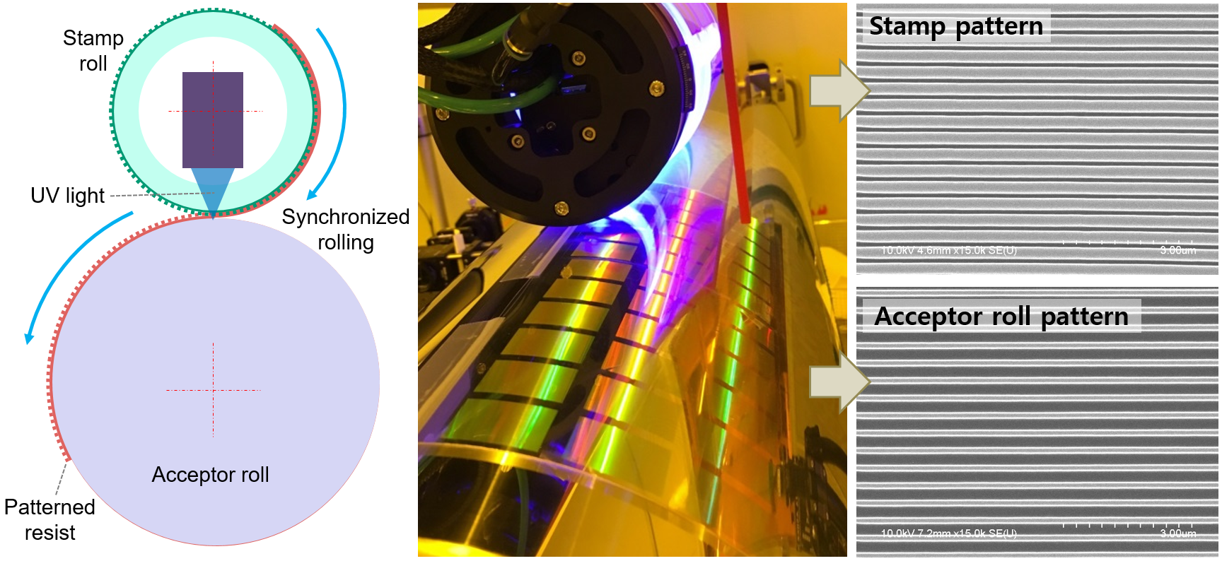
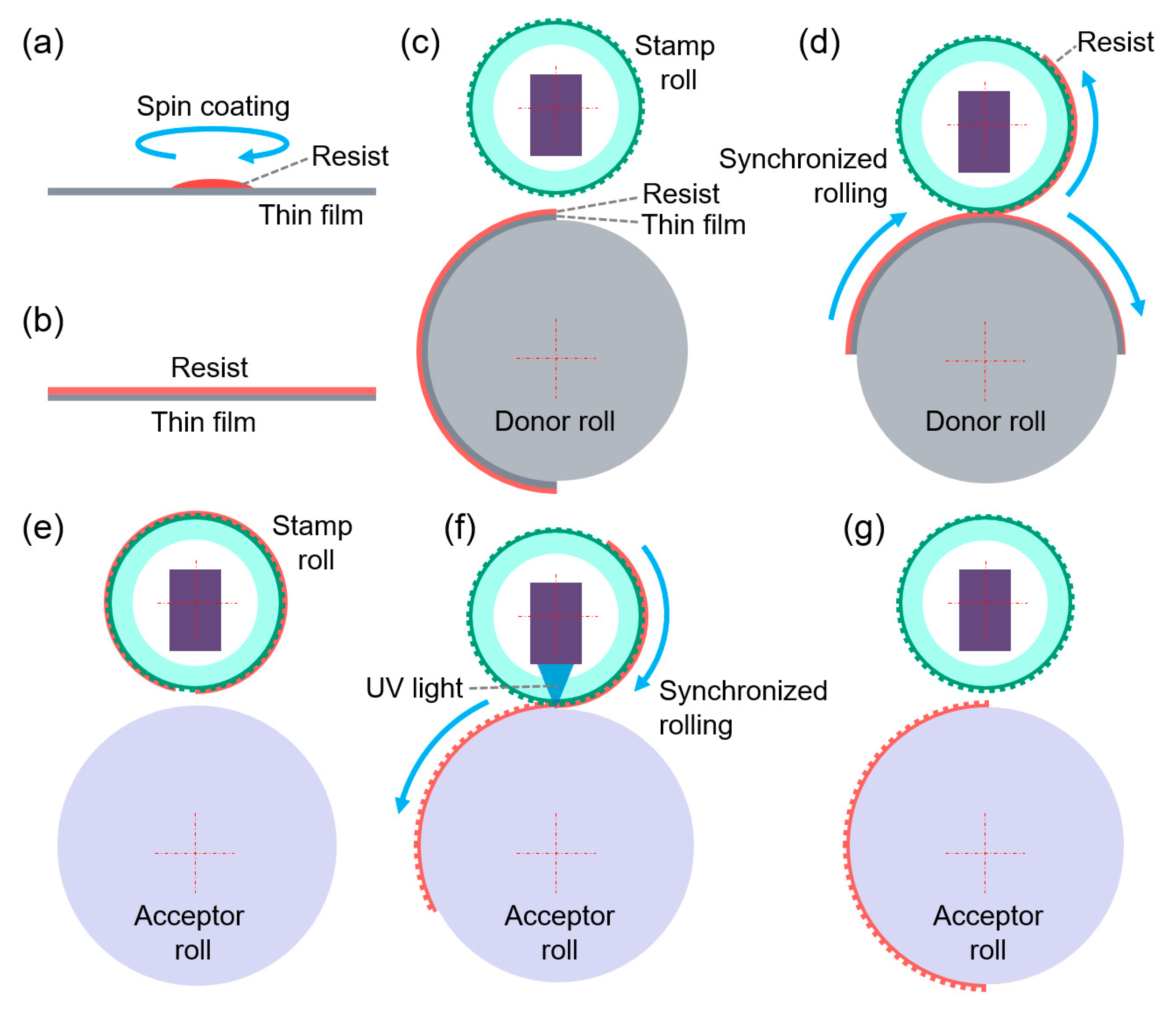
2.1. Process Design for Fabrication Large-Area Roll Molds
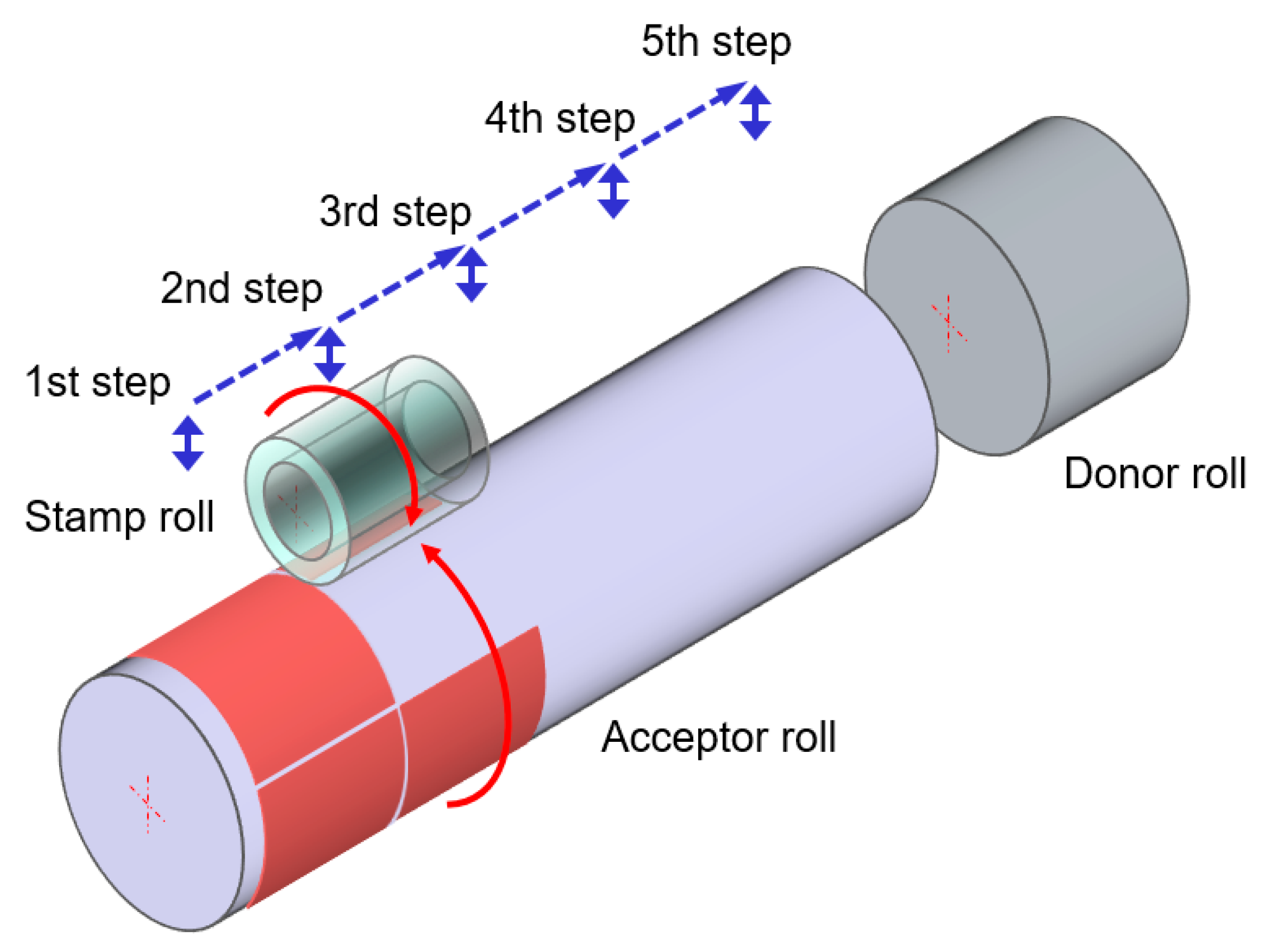
2.2. Step-and-Repeat Process
3. Experiments
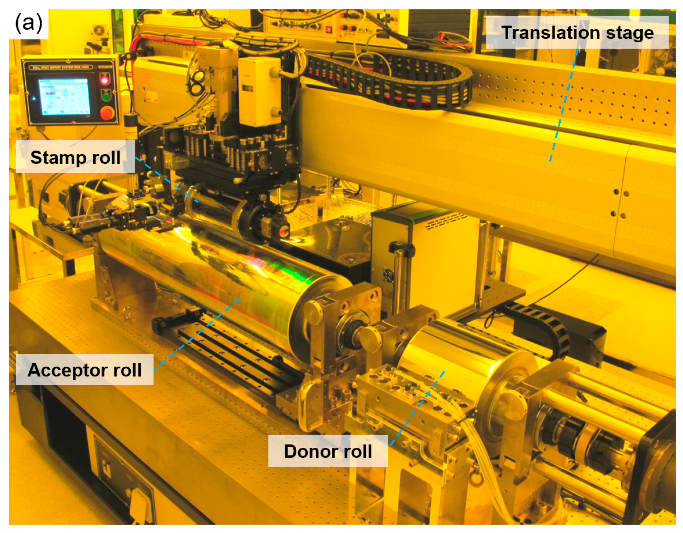
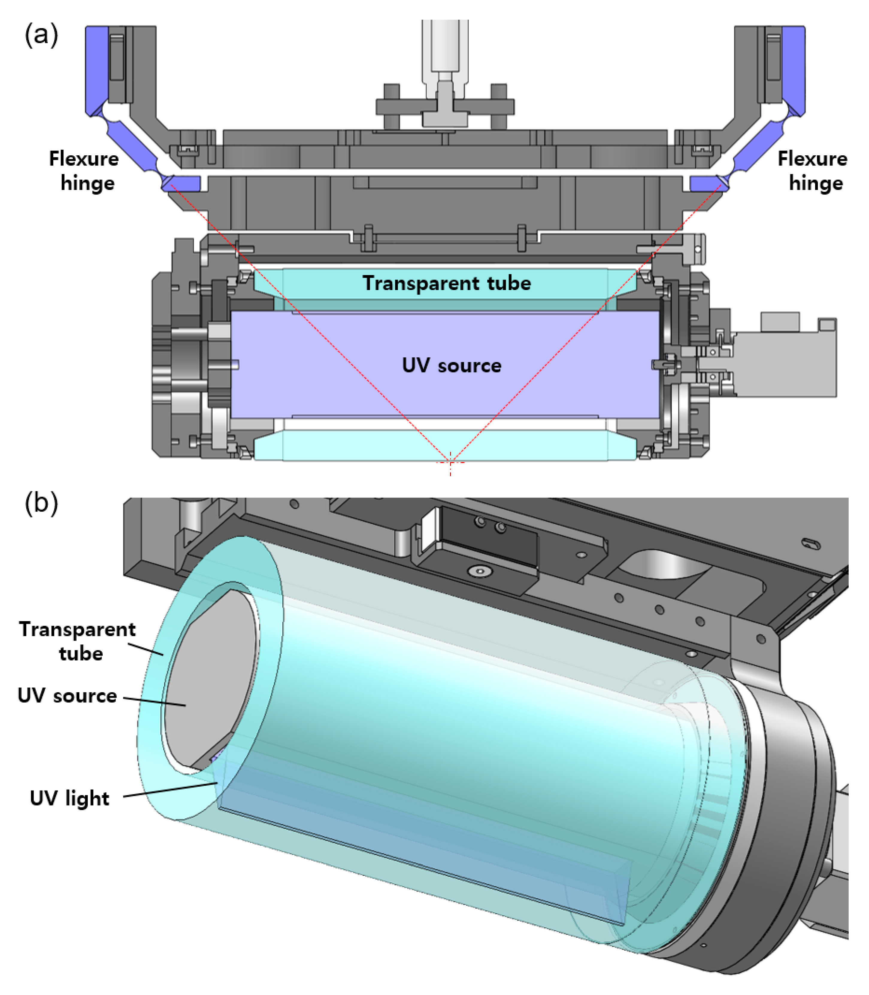
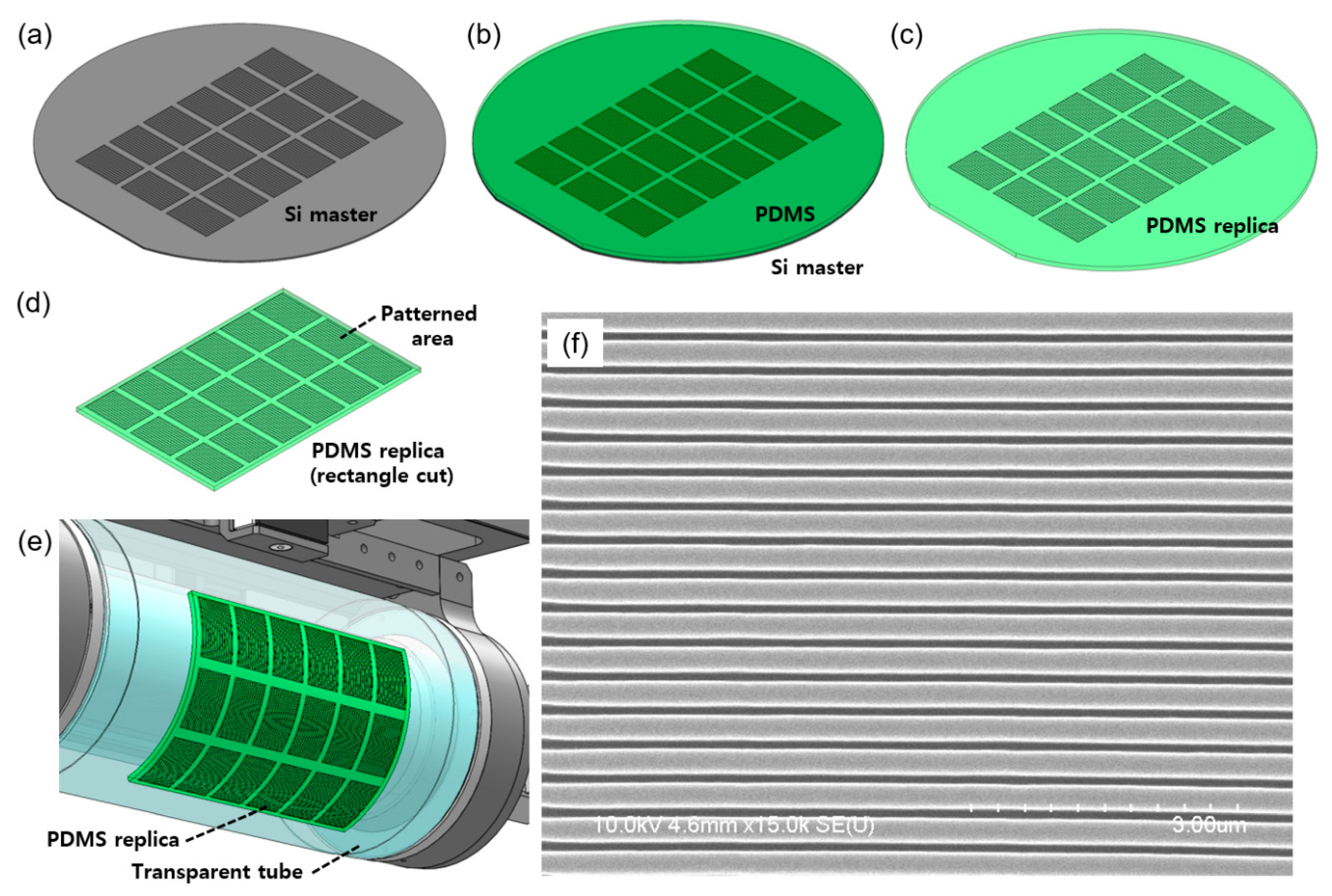
3.1. System
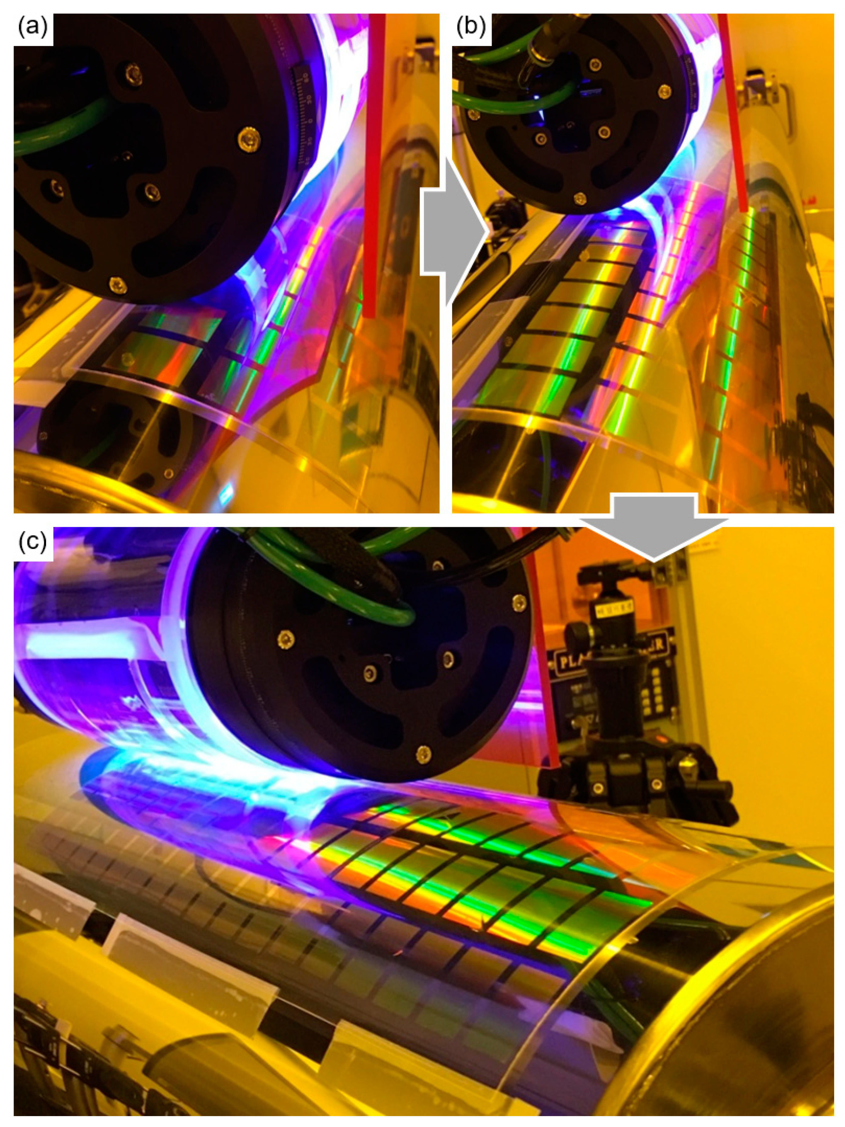
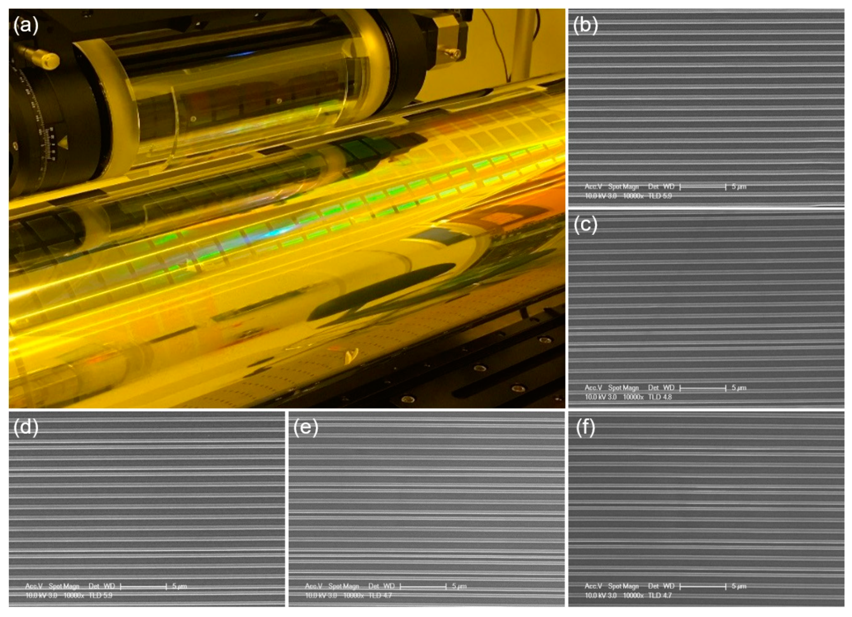
3.2. Patterning
4. Discussion
5. Conclusions
Author Contributions
Funding
Conflicts of Interest
References
- Ahn, S.H.; Guo, L.J. Large-area roll-to-roll and roll-to-plate nanoimprint lithography: A step toward high-throughput application of continuous nanoimprinting. ACS Nano 2009, 3, 2304–2310. [Google Scholar] [CrossRef]
- Han, J.; Choi, S.; Lim, J.; Lee, B.S.; Kang, S. Fabrication of transparent conductive tracks and patterns on flexible substrate using a continuous UV roll imprint lithography. J. Phys. D Appl. Phys. 2009, 42, 115503. [Google Scholar] [CrossRef]
- Nagato, K.; Sugimoto, S.; Hamaguchi, T.; Nakao, M. Iterative roller imprint of multilayered nanostructures. Microelectron. Eng. 2010, 87, 1543–1545. [Google Scholar] [CrossRef]
- Dumond, J.J.; Mahabadi, K.A.; Yee, Y.S.; Tan, C.; Fuh, J.Y.H.; Lee, H.P.; Low, H.Y. High resolution UV roll-to-roll nanoimprinting of resin moulds and subsequent replication via thermal nanoimprint lithography. Nanotechnology 2012, 23, 485310. [Google Scholar] [CrossRef] [PubMed]
- Ok, J.G.; Youn, H.S.; Kwak, M.K.; Lee, K.T.; Shin, Y.J.; Guo, L.J.; Greenwald, A.; Liu, Y. Continuous and scalable fabrication of flexible metamaterial films via roll-to-roll nanoimprint process for broadband plasmonic infrared filters. Appl. Phys. Lett. 2012, 101, 223102. [Google Scholar] [CrossRef]
- Yoshikawa, H.; Taniguchi, J.; Tazaki, G.; Zento, T. Fabrication of high-aspect-ratio pattern via high throughput roll-to-roll ultraviolet nanoimprint lithography. Microelectron. Eng. 2013, 112, 273–277. [Google Scholar] [CrossRef]
- Jiang, M.; Lin, S.; Jiang, W.; Pan, N. Hot embossing holographic images in BOPP shrink films throughlarge-area roll-to-roll nanoimprint lithography. Appl. Surf. Sci. 2014, 311, 101–106. [Google Scholar] [CrossRef]
- Mäkelä, T.; Kainlauri, M.; Willberg-Keyriläinen, P.; Tammelin, T.; Forsström, U. Fabrication of micropillars on nanocellulose films using a roll-to-roll nanoimprinting method. Microelectron. Eng. 2016, 163, 1–6. [Google Scholar] [CrossRef]
- Leitgeb, M.; Nees, D.; Ruttloff, S.; Palfinger, U.; Götz, J.; Liska, R.; Belegratis, M.R.; Stadlober, B. Multilength Scale Patterning of Functional Layers by Roll-to-Roll Ultraviolet-Light-Assisted Nanoimprint Lithography. ACS Nano 2016, 10, 4926–4941. [Google Scholar] [CrossRef]
- Retolaza, A.; Juarros, A.; Ramiro, J.; Merino, S. Thermal roll to roll nanoimprint lithography for micropillars fabrication on thermoplastics. Microelectron. Eng. 2018, 193, 54–61. [Google Scholar] [CrossRef]
- Lee, S.-B.; Ji, S.; Lee, J.-Y.; Lee, J.; Yeo, J.-S. Fluorinated low-viscosity copolymer with enhanced release property for roll-to-plate UV nanoimprint lithography. Nanotechnology 2019, 30, 505301. [Google Scholar] [CrossRef]
- Taniguchi, J.; Aratani, M. Fabrication of a seamless roll mold by direct writing with an electron beam on a rotating cylindrical substrate. J. Vac. Sci. Technol. B 2009, 27, 2841–2845. [Google Scholar] [CrossRef]
- Maruyama, H.; Unno, N.; Taniguchi, J. Fabrication of roll mold using electron-beam direct writing and metal lift-off process. Microelectron. Eng. 2012, 97, 113–116. [Google Scholar] [CrossRef]
- Huang, K.-F.; Lee, Y.-C. Fabrication of metal roller mold with submicrometer feature size using contact printing photolithography technique. J. Vac. Sci. Technol. B Nanotechnol. Microelectron. 2013, 31, 031604. [Google Scholar] [CrossRef]
- Tsai, S.-W.; Chen, P.-Y.; Lee, Y.-C. Fabrication of a seamless roller mold with wavy microstructures using mask-less curved surface beam pen lithography. J. Micromech. Microeng. 2014, 24, 045022. [Google Scholar] [CrossRef]
- Tahir, U.; Kamran, M.A.; Jang, M.H.; Jeong, M.Y. Thin-film coating on cylinder for fabrication of cylindrical mold: Roll-to-roll nano-imprint lithography. Microelectron. Eng. 2019, 211, 5–12. [Google Scholar] [CrossRef]
- Koo, N.; Kim, J.W.; Otto, M.; Moormann, C.; Kurz, H. Liquid transfer imprint lithography: A new route to residual layer thickness control. J. Vac. Sci. Technol. B 2011, 29. [Google Scholar] [CrossRef]
- Lee, J.; Park, H.; Choi, K.; Kim, G.; Lim, H. Fabrication of hybrid structures using UV roll-typed liquid transfer imprint lithography for large areas. Microelectron. Eng. 2014, 127, 72–76. [Google Scholar] [CrossRef]
- Moro, M.; Taniguchi, J. Removal of residual layer by liquid transfer imprint lithography using roll-to-roll UV-NIL. Microelectron. Eng. 2015, 141, 112–116. [Google Scholar] [CrossRef]
- Uchida, T.; Yu, F.; Nihei, M.; Taniguchi, J. Fabrication of antireflection structures on the surface of optical lenses by using a liquid transfer imprint technique. Microelectron. Eng. 2016, 153, 43–47. [Google Scholar] [CrossRef]
- Unno, N.; Kigami, H.; Fujinami, T.; Nakata, S.; Satake, S.; Taniguchi, J. Fabrication of calibration plate for total internal reflection fluorescence microscopy using roll-type liquid transfer imprint lithography. Microelectron. Eng. 2017, 180, 86–92. [Google Scholar] [CrossRef]
- Lim, H.; Choi, K.; Kim, G.; Lee, S.; Park, H.; Ryu, J.; Jung, S.; Lee, J. Roll-to-roll nanoimprint lithography for patterning on a large-area substrate roll. Microelectron. Eng. 2014, 123, 18–22. [Google Scholar] [CrossRef]

© 2020 by the authors. Licensee MDPI, Basel, Switzerland. This article is an open access article distributed under the terms and conditions of the Creative Commons Attribution (CC BY) license (http://creativecommons.org/licenses/by/4.0/).
Share and Cite
Lim, H.; Jung, S.; Ahn, J.; Choi, K.-B.; Kim, G.; Kwon, S.; Lee, J. System for Fabrication of Large-Area Roll Molds by Step-and-Repeat Liquid Transfer Imprint Lithography. Materials 2020, 13, 1938. https://doi.org/10.3390/ma13081938
Lim H, Jung S, Ahn J, Choi K-B, Kim G, Kwon S, Lee J. System for Fabrication of Large-Area Roll Molds by Step-and-Repeat Liquid Transfer Imprint Lithography. Materials. 2020; 13(8):1938. https://doi.org/10.3390/ma13081938
Chicago/Turabian StyleLim, Hyungjun, Sanghee Jung, Junhyoung Ahn, Kee-Bong Choi, Geehong Kim, Soongeun Kwon, and Jaejong Lee. 2020. "System for Fabrication of Large-Area Roll Molds by Step-and-Repeat Liquid Transfer Imprint Lithography" Materials 13, no. 8: 1938. https://doi.org/10.3390/ma13081938
APA StyleLim, H., Jung, S., Ahn, J., Choi, K.-B., Kim, G., Kwon, S., & Lee, J. (2020). System for Fabrication of Large-Area Roll Molds by Step-and-Repeat Liquid Transfer Imprint Lithography. Materials, 13(8), 1938. https://doi.org/10.3390/ma13081938