Numerical Investigation of the Impact of ITO, AlInN, Plasmonic GaN and Top Gold Metalization on Semipolar Green EELs

 ,
,  , , , and
Abstract
1. Introduction
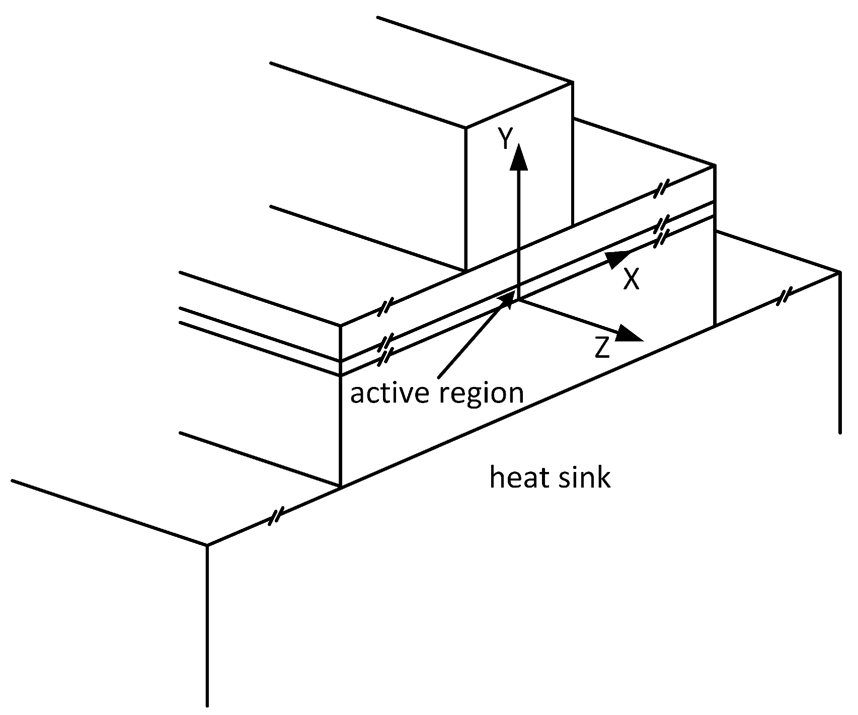
2. The Model
2.1. The Electrical Model
2.2. The Thermal Model
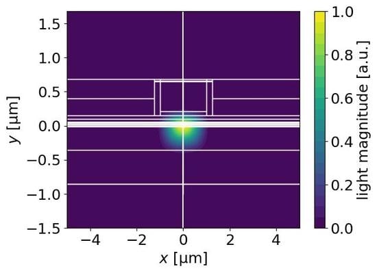
2.3. The Optical Model
2.4. The Gain Model
2.5. Interactions between Individual Physical Phenomena
- temperature and carrier-concentration dependencies of electrical conductivities,
- temperature dependence of recombination coefficients,
- temperature dependence of thermal conductivities,
- temperature dependence of energy gaps,
- temperature, wavelength and carrier-concentration dependencies of refractive indices and absorption coefficients,
- the effect of the spontaneous and piezoelectric polarizations on the band structure of the active region.
3. Modeled Structures and Parameters
3.1. Top Metalization
3.2. EEL ITO
3.3. EEL ITO/GaN++
3.4. EEL ITO/AlInN
4. Conclusions
Author Contributions
Funding
Conflicts of Interest
References
- Sizov, D.; Bhat, R.; Wang, J.; Allen, D.; Paddock, B.; Zah, C. Development of semipolar laser diode. Phys. Status Solidi A 2013, 210, 459–465. [Google Scholar] [CrossRef]
- Hardy, M.T.; Wu, F.; Hsu, P.S.; Haeger, D.A.; Nakamura, S.; Speck, J.S.; DenBaars, S.P. True green semipolar InGaN-based laser diodes beyond critical thickness limits using limited area epitaxy. J. Appl. Phys. 2013, 114, 183101. [Google Scholar] [CrossRef]
- Pourhashemi, A.; Farrell, R.M.; Cohen, D.A.; Speck, J.S.; DenBaars, S.P.; Nakamura, S. High-power blue laser diodes with indium tin oxide cladding on semipolar (2021) GaN substrates. Appl. Phys. Lett. 2015, 106, 111105. [Google Scholar] [CrossRef]
- Schenk, H.P.D.; Nemoz, M.; Korytov, M.; Vennéguès, P.; Demolon, P.; Dräger, A.D.; Hangleiter, A.; Charash, R.; Maaskant, P.P.; Corbett, B.; Duboz, J.Y. AlInN optical confinement layers for edge emitting group III-nitride laser structures. Phys. Status Solidi C 2009, 6, S897–S901. [Google Scholar] [CrossRef]
- Stańczyk, S.; Czyszanowski, T.; Kafar, A.; Czernecki, R.; Targowski, G.; Leszczyński, M.; Suski, T.; Kucharski, R.; Perlin, P. InGaN laser diodes with reduced AlGaN cladding thickness fabricated on GaN plasmonic substrate. Appl. Phys. Lett. 2013, 102, 151102. [Google Scholar] [CrossRef]
- Hardy, M.T.; Holder, C.O.; Feezell, D.F.; Nakamura, S.; Speck, J.S.; Cohen, D.A.; DenBaars, S.P. Indium-tin-oxide clad blue and true green semipolar InGaN/GaN laser diodes. Appl. Phys. Lett. 2013, 103, 081103. [Google Scholar] [CrossRef]
- Chiang, K.S. Analysis of optical fibers by the effective index method. Appl. Opt. 1986, 25, 348–354. [Google Scholar] [CrossRef]
- Chuang, S.L. Physics of Photonic Devices; John Wiley & Sons: Hoboken, NJ, USA, 2009; pp. 350–352. [Google Scholar]
- Bugajski, M. Optical gain in quantum well lasers including many-body effects. Electron Technol. 1997, 30, 89–98. [Google Scholar]
- Kuc, M.; Sarzała, R.P.; Nakwaski, W. Thermal crosstalk in arrays of III-N-based Lasers. Mater. Sci. Eng. B 2013, 178, 1395–1402. [Google Scholar] [CrossRef]
- Kuc, M.; Sarzała, R.P.; Stańczyk, S.; Perlin, P. Numerical investigation of an impact of a top gold metallization on output power of a p-up III-N-based blue-violet edge-emitting laser diode. Opto-Electron. Rev. 2015, 23, 131–136. [Google Scholar] [CrossRef]
- Kuc, M.; Piskorski, Ł.; Sokół, A.K.; Dems, M.; Wasiak, M.; Sarzała, R.P.; Czyszanowski, T. Optical simulations of blue and green semipolar InGaN/GaN lasers. Proc. SPIE 2018, 10532, 1053228. [Google Scholar]
- Swietlik, T.; Franssen, G.; Czernecki, R.; Leszczyński, M.; Skierbiszewski, C.; Grzegory, I.; Suski, T.; Perlin, P.; Lauterbach, C.; Schwarz, U.T. Mode dynamics of high power (InAl)GaN based laser diodes grown on bulk GaN substrate. J. Appl. Phys. 2007, 101, 083109. [Google Scholar] [CrossRef]
- Malinverni, M.; Lamy, J.-M.; Martin, D.; Lahourcade, L.; Feltin, E.; Dorsaz, J.; Castiglia, A.; Rossetti, M.; Duelk, M.; Vélez, C.; Grandjean, N. InGaN laser diodes emitting at 500 nm with p-layers grown by molecular beam epitaxy. Appl. Phys. Express 2015, 8, 022105. [Google Scholar] [CrossRef]
- Beechem, T.E.; McDonald, A.E.; Fuller, E.J.; Talin, A.A.; Rost, C.M.; Maria, J.-P.; Gaskins, J.T.; Hopkins, P.E.; Allerman, A.A. Size dictated thermal conductivity of GaN. J. Appl. Phys. 2016, 120, 095104. [Google Scholar] [CrossRef]
- Kuc, M.; Sokół, A.K.; Piskorski, Ł.; Dems, M.; Wasiak, M.; Sarzała, R.P.; Czyszanowski, T. ITO layer as an optical confinement for nitride edge-emitting lasers. Bull. Pol. Acad. Sci. 2020, 68, 147–154. [Google Scholar]
- Soltani, M.; Soref, R.; Palacios, T.; Englund, D. AlGaN/AlN integrated photonics platform for the ultraviolet and visible spectral range. Opt. Express 2016, 24, 25415–25423. [Google Scholar] [CrossRef]
- Watanabe, N.; Kimoto, T.; Suda, J. The temperature dependence of the refractive indices of GaN and AlN from room temperature up to 515 ∘C. J. Appl. Phys. 2008, 104, 106101. [Google Scholar] [CrossRef]
- Carlin, J.-F.; Zellweger, C.; Dorsaz, J.; Nicolay, S.; Christmann, G.; Feltin, E.; Butté, R.; Grandjean, N. Progresses in III-nitride distributed Bragg reflectors and microcavities using AlInN/GaN materials. Phys. Stat. Sol. B 2005, 242, 2326–2344. [Google Scholar] [CrossRef]
- Kuramoto, M.; Sasaoka, C.; Futagawa, N.; Nido, M.; Yamaguchi, A.A. Reduction of internal loss and threshold current in a laser diode with a ridge by selective re-growth (RiS-LD). Phys. Stat. Sol. A 2002, 192, 329–334. [Google Scholar] [CrossRef]
- Oshima, Y.; Yoshida, T.; Watanabe, K.; Mishima, T. Properties of Ge-doped, high-quality bulk GaN crystals fabricated by hydride vapor phase epitaxy. J. Cryst. Growth 2010, 312, 3569–3573. [Google Scholar] [CrossRef]
- Brunner, D.; Angerer, H.; Bustarret, E.; Freudenberg, F.; Höpler, R.; Dimitrov, R.; Ambacher, O.; Stutzmann, M. Optical constants of epitaxial AlGaN films and their temperature dependence. J. Appl. Phys. 1997, 82, 5090–5096. [Google Scholar] [CrossRef]
- Ueno, K.; Arakawa, Y.; Kobayashi, A.; Ohta, J.; Fujioka, H. Highly conductive Ge-doped GaN epitaxial layers prepared by pulsed sputtering. Appl. Phys. Express 2017, 10, 101002. [Google Scholar] [CrossRef]
- Miyoshi, M.; Yamanaka, M.; Egawa, T.; Takeuchi, T. Epitaxial growth and characterization of approximately 300-nm-thick AlInN films nearly lattice-matched to c-plane GaN grown on sapphire. Appl. Phys. Express 2018, 11, 051001. [Google Scholar] [CrossRef]


| layer | Material | Thickness [μm] |
|---|---|---|
| p-contact | Ti/Au | 0.03/1 |
| isolation | SiO2 | 0.25 |
| p-cladding | ITO/p-GaN | 0.28/0.27 |
| p-waveguide | p-InGaN | 0.045 |
| EBL | p-AlGaN | 0.010 |
| active region | MQW InGaN/GaN | 0.0027/0.01 |
| n-waveguide | n-InGaN | 0.010 |
| n-cladding | n-GaN | 0.55 |
| substrate | n-GaN | 50 |
| n-contact | Al/Au | 0.03/0.3 |
| Material | Doping | Thickness | ||||
|---|---|---|---|---|---|---|
| [cm−3] | [μm] | [W/(m·K)] | [W/(m·K)] | [S/m] | [S/m] | |
| p-GaN | Mg: | 0.21–0.37 | 92 | 61 | 95 | 309 |
| p-InGaN | Mg: | 0.045 | 23 | 20 | 284 | 280 |
| p-AlGaN | Mg: | 0.010 | 13 | 12 | 22 | 70 |
| n-GaN (substrate) | Si: | 50 | 166 | 110 | ||
| n-InGaN | Si: | 0.01 | 28 | 26 | 636 | 703 |
| n-AlInN | Si-doped | 0.1–0.5 | 5 | 5 | ||
| n-GaN (plasmonic) | Ge: | 0.05–0.50 | 54 | 36 | ||
| n-GaN (plasmonic) | Ge: | 0.05–0.50 | 35 | 24 | ||
| n-GaN (plasmonic) | Ge: | 0.05–0.50 | 23 | 16 | ||
| n-GaN (plasmonic) | Ge: | 0.05–0.50 | 10 | 7 | ||
| GaN (barrier) | undoped | 0.010 | 61 | 41 | 255 | 242 |
| n-InGaN (QW) | Si-doped | 0.0027 | 2 | 2 | 250 | 278 |
| SiO2 | n/a | 0.25 | 1 | 1 | ||
| ITO | n/a | 0.18–0.44 | 3 | 3 | ||
| Au | n/a | 0.1–3.0 | 316 | 311 | ||
| Al | n/a | 0.03 | 180 | 180 | ||
| Ti | n/a | 0.03 | 22 | 20 | ||
| PbSn | n/a | 1 | 50 | 50 | ||
| Cu | n/a | 5000 | 403 | 393 |
| Material | [1/cm] | [1/cm] | ||
|---|---|---|---|---|
| p-GaN | 2.3787 | 2.3881 | 100 | 100 |
| p-InGaN | 2.4429 | 2.4530 | 100 | 100 |
| p-AlGaN | 2.3099 | 2.3181 | 100 | 100 |
| n-GaN | 2.3787 | 2.3881 | 10 | 10 |
| p-InGaN | 2.4429 | 2.4530 | 10 | 10 |
| n-AlInN | 2.2202 | 2.2260 | 23 | 23 |
| n-GaN (Ge: ) | 2.2179 | 2.2267 | 870 | 870 |
| n-GaN (Ge: ) | 2.0445 | 2.0526 | 1745 | 1745 |
| n-GaN (Ge: ) | 1.8550 | 1.8623 | 2615 | 2615 |
| n-GaN (Ge: ) | 1.4009 | 1.4065 | 4350 | 4350 |
| n-InGaN (QW) | 2.7310 | 2.7431 | gain | gain |
| SiO | 1.4795 | 1.4795 | 0 | 0 |
| ITO | 1.9357 | 1.9357 | 1920 | 1920 |
| Au | 0.3710 | 0.3710 | ||
| Ti | 2.5081 | 2.5081 |
| Γ | |||||
|---|---|---|---|---|---|
| [cm−3] | [μm] | [μm] | [μm] | [kA/cm2] | [%] |
| 1 × 10 | 0.50 | 0.65 | 0.39 | 8.39 | 9.8 |
| 2 × 10 | 0.30 | 0.60 | 0.40 | 7.87 | 10.5 |
| 3 × 10 | 0.25 | 0.55 | 0.41 | 7.56 | 11.2 |
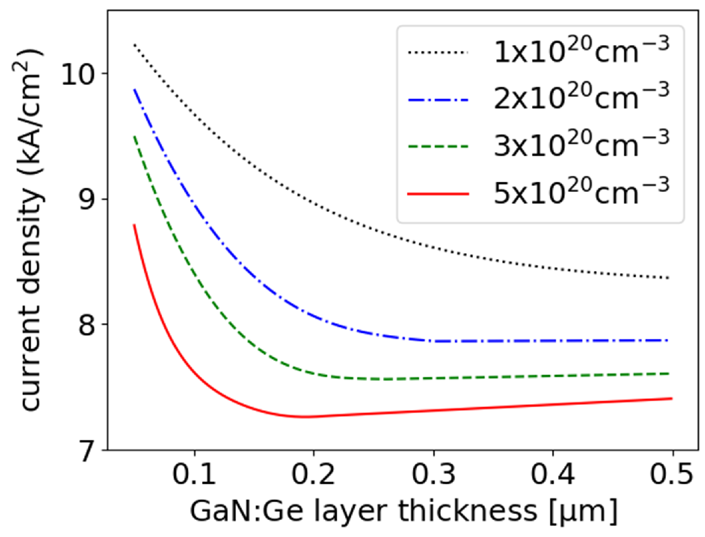
| 5 × 10 | 0.20 | 0.50 | 0.42 | 7.26 | 12.1 |
| Γ | ||||
|---|---|---|---|---|
| [μm] | [μm] | [μm] | [kA/cm2] | [%] |
| 0.1 | 0.85 | 0.30 | 9.10 | 9.0 |
| 0.3 | 0.50 | 0.41 | 7.26 | 11.2 |
| 0.5 | 0.35 | 0.44 | 6.69 | 13.6 |
© 2020 by the authors. Licensee MDPI, Basel, Switzerland. This article is an open access article distributed under the terms and conditions of the Creative Commons Attribution (CC BY) license (http://creativecommons.org/licenses/by/4.0/).
Share and Cite
Kuc, M.; Piskorski, Ł.; Dems, M.; Wasiak, M.; Sokół, A.K.; Sarzała, R.P.; Czyszanowski, T. Numerical Investigation of the Impact of ITO, AlInN, Plasmonic GaN and Top Gold Metalization on Semipolar Green EELs. Materials 2020, 13, 1444. https://doi.org/10.3390/ma13061444
Kuc M, Piskorski Ł, Dems M, Wasiak M, Sokół AK, Sarzała RP, Czyszanowski T. Numerical Investigation of the Impact of ITO, AlInN, Plasmonic GaN and Top Gold Metalization on Semipolar Green EELs. Materials. 2020; 13(6):1444. https://doi.org/10.3390/ma13061444
Chicago/Turabian StyleKuc, Maciej, Łukasz Piskorski, Maciej Dems, Michał Wasiak, Adam K. Sokół, Robert P. Sarzała, and Tomasz Czyszanowski. 2020. "Numerical Investigation of the Impact of ITO, AlInN, Plasmonic GaN and Top Gold Metalization on Semipolar Green EELs" Materials 13, no. 6: 1444. https://doi.org/10.3390/ma13061444
APA StyleKuc, M., Piskorski, Ł., Dems, M., Wasiak, M., Sokół, A. K., Sarzała, R. P., & Czyszanowski, T. (2020). Numerical Investigation of the Impact of ITO, AlInN, Plasmonic GaN and Top Gold Metalization on Semipolar Green EELs. Materials, 13(6), 1444. https://doi.org/10.3390/ma13061444