Abstract
We report herein high-resolution X-ray diffraction measurements of basal plane bending of homoepitaxial single-crystal diamond (SCD). We define SCD (100) as the base plane. The results revealed that growth parameters such as temperature, growth time, and basal plane bending of the substrate all affect the basal plane bending of SCD. First, the basal plane bending of SCD depends mainly on the substrate and becomes severe with increasing basal plane bending of the substrate. The SCD growth experiments show that the basal plane bending increases with elevated growth temperature and increased growth time. Finally, to understand the mechanism, we investigated the substrate-surface temperature distribution as a function of basal plane bending of SCD fabricated by chemical vapor deposition (CVD). This allowed us to propose a model and understand the origin of basal plane bending. The results indicate that an uneven temperature distribution on the substrate surface is the main cause of the base-plane bending of CVD diamond.
1. Introduction
Single-crystal diamond (SCD) has a wide band gap, high thermal conductivity, high breakdown voltage, high carrier mobility, and strong resistance to radiation, which earns it the name “the ultimate semiconductor” [1,2,3,4,5,6]. It can be used in deep ultraviolet detectors, particle detectors, high-power, high-voltage. and high-frequency electronics, etc. [7,8]. Motivated by these promising applications, the growth of large-size, high-quality SCD by high pressure high temperature (HTHP) and microwave plasma chemical vapor deposition (MPCVD) has become an important research topic [9,10].
The MPCVD technique has now led to the fabrication of 2-inch mosaic SCDs. In parallel with the improvement on SCD size, improving the quality assessment of SCDs becomes important for their use as semiconductor devices. In general, basal plane bending in SCDs degrades the crystal quality by inducing dislocations and even cracks [11,12,13,14]. In addition, the relationship between basal plane bending and growth parameters has been studied. Hock et al. [15] investigated in situ lattice plane bending during crystal growth and demonstrated that lattice-plane bending and thermo-elastic stress vary with growth rate. Yang et al. found that substrate attachment strongly affects basal plane bending and plastic-deformation-induced dislocations [11]. Sumathi [16] used X-ray diffraction to obtain a basal plane bending of 100 arcsec in AlN, which suggests a high structural homogeneity in the crystals. However, no reports yet exist on basal plane bending in SCDs.
This work thus presents a detailed X-ray diffraction study of the basal plane bending in homoepitaxial SCD deposited by MPCVD. The results indicated that spatial variations of basal plane bending are approximately spherical. In addition, we discuss how the growth temperature, the substrate quality and the growth time affected the bending radius. Furthermore, we propose a mechanism whereby the temperature gradient affects basal plane bending in SCD.
2. Materials and Methods
Basal plane bending was measured by using a Bruker D8 Discover high-resolution X-ray diffractometer (HRXRD) (D8 Discover, Bruker, Germany) operating with Cu Kα1 radiation at 40 kV with a current of 40 mA. The X-ray beam was scanned in 1 mm steps from one edge of the substrate to the other.
We applied the basic principle of X-ray diffraction to detect basal plane bending [17,18]. When the basal plane is flat, the normal of the diffraction plane remains the same regardless of the beam positions. As a result, the angle of incidence is independent of the beam position (ω1 = ω2 = ω3; where ω is the angle between the incident beam and the sample surface), as shown in Figure 1b. However, when the basal plane is bent, the normal orientation of the diffraction plane will vary with the beam positions. For a convex (concave) basal plane, as shown in Figure 1a,c, the angle of incidence increases (decreases) monotonically as the X-ray beam is scanned over the sample surface, so ω1 < ω2 < ω3 (ω1 > ω2 > ω3). Figure 2 depicts the variation of relative ω(400) rocking curve peak position along with the beam position across one side to another side of the diamond plate. Upon scanning in a given direction from one edge of the wafer to the other, ω gradually changes and the bent basal plane forms an approximately spherical surface. Using the slope of ω as a function of scanning distance x, ω gradually changes and the bent basal plane forms an approximately spherical surface. From the slope of ω as a function of scanning distance x, the radius R of the bending plane is given by
where R [19] is the radius of the basal plane in the plane of diffraction and ω is measured in radians.
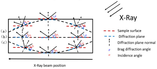
Figure 1.
Schematic diagram of HRXRD measurement of basal plane bending. Panels (a)–(c) show that the basal planes are convex, flat, and concave, respectively.
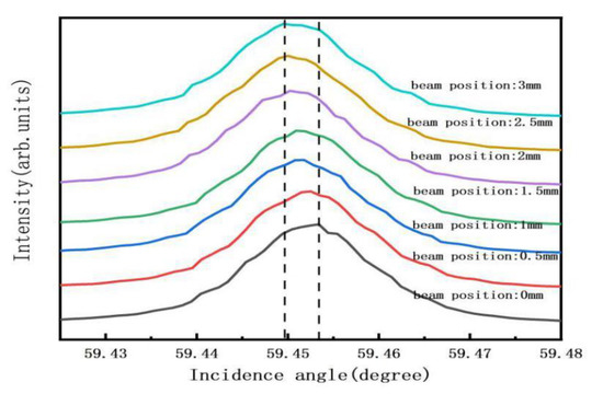
Figure 2.
(400) rocking curves at different positions by HRXRD measurement.
The MPCVD used in our studies is ARDIS-300 made by Optosystems Ltd. (Moscow, Russia) equipped with a 2.45 GHz/6 kW microwave reactor. A detailed description of the chamber geometry and the deposition reaction system is given by Wang [20]. A double interference infrared radiation thermo pyrometer is installed to measure the temperature of the substrate with an emissivity of 0.1 through a slit of 2 mm. The substrate surface temperature was maintained by self-adjusting the microwave power input through feedback from the thermo pyrometer. We measured the temperature distribution by moving the thermometer installed on a three-dimensional displacement platform.
Three groups of experiments were carried out. Table 1, Table 2 and Table 3 summarize the growth conditions. To compare how the substrate affects basal plane bending, we used (100)-oriented HTHP and MPCVD SCD as substrates for sample H and M. The substrates were purchased from Jinan Zhongwu New Material Co. Ltd. (Jinan, Shandong, China). For SCD growth, the concentration ratio of methane to hydrogen was 3%, the pressure was 275 torr and the growth time was 4 h. The samples labelled H1–H4 were grown separately at 900, 1000, 1100, and 1150 °C, respectively. Table 2 details the growth conditions. Table 3 is for sample H3, which was grown in three cycles. After each growth period of 4 h, HRXRD was used to evaluate how growth time affects basal plane bending.

Table 1.
Sample growth conditions on HTHP and MPCVD diamonds.
Table 2.
Sample growth conditions on HTHP diamonds at different temperatures.
Table 3.
Sample growth conditions on HTHP diamonds for different growth times.
3. Results and Discussion
For sample H1 and M1, the basal plane bending was measured before MPCVD growth and after growth. Figure 3 shows the relative ω (Δω400) peak positions as a function of beam positions. As the beam moves from one edge of the substrate to the other, the relative ω (Δω400) peak positions decrease linearly, which indicates spherical bending of the basal plane. The shifts in peak position before and after the MPCVD growth of the H1 sample were 14.76 arcsec and 2.88 arcsec and the corresponding radius of the basal plane bending 74.05 and 358.17 m, respectively.
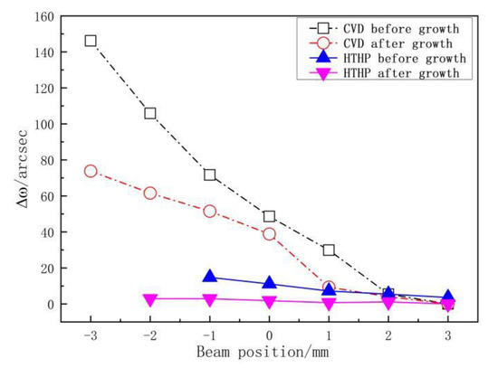
Figure 3.
Peak position of ω(Δω400) as a function of beam positions on the diamond plane.
The peak positions of sample M1 before and after growth were 146.16 arcsec and 73.80 arcsec, respectively, which correspond to basal plane curvature radius of 8.47 and 16.78 m. The results show that (1) the curvature radius of SCD after MPCVD growth is closely related to the substrate curvature, (2) the curvature radius of SCD grown on a HTHP substrate is much greater than that of SCD grown on a MPCVD substrate. The plane bending of SCD is inherited from the substrate, which indicates that the substrate plays an important role in determining the SCD basal plane bending. This mechanism is similar to dislocations inheredity which can propagate from the substrate to the epilayer. To reduce the basal plane bending thus requires the use of high-quality substrates without basal plane bending.
For SCD grown on the HTHP substrate, the basal plane bending radius exceeds 50 m. We investigated how growth temperature and growth time affected the basal plane bending. Figure 4a shows relative ω(Δω400) peak positions as a function of beam position for samples H1 to H4. The slope of the curve increases with growth temperature, which translates into a reduced radius of curvature of the SCD base plane. As shown in Figure 4b, the radius of the SCD basal plane curvature decreases monotonically with increasing growth temperature. At a growth temperature of 1150 °C, the radius of the basal plane curvature reaches its minimum of 23.40 m.
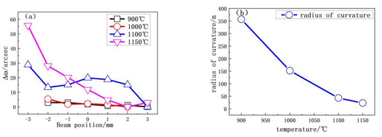
Figure 4.
(a) Peak position of ω(Δω400) as a function of beam position at several different temperatures. (b) Radius of curvature as a function of the growth temperatures.
For sample H3, the relative ω(Δω400) peak positions do not decrease linearly. However, with increasing growth time at a given growth temperature, the slope of the curve gradually increases (see Figure 5a). As shown in Figure 5b, the radius of basal plane curvature is 10.20 m for a total growth time of 16 h. Thus, longer growth time leads to more severe basal plane bending.
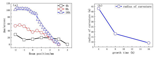
Figure 5.
(a) Relative position ω(Δω400) as a function of X-ray beam position on the diamond plane for different growth times. (b) Radius of curvature as a function of the growth time.
These results all indicate that the basal plane bending of SCD is affected by temperature, growth time, and substrate. In addition, the basal plane bending is related to the temperature gradient and the substrate attachment. Ha et al. [21] used the finite-element method ANSYS software (Swanson Analysis Systems, Inc, Canonsburg, PA, USA) to simulate the stress distribution during the growth of free and solid seeds and proposed that negative shear stress generates base dislocations in the crystal. By conducting a symmetric Laue geometry transmission test on a primary single crystal containing nitrogen-doped stripes obtained under different growth conditions, Seitz et al. [17] found that the basal plane bending of the single-crystal front end was consistent with the isotherm of the single crystal. In MPCVD growth, the SCD substrate uses open backside attachment, so substrate attachment is not the source of the bending. Based on the model proposed by Harris and Goodwin [22,23,24]. Silva et al. [25] simulated the temperature distribution in the SCD growth chamber and found a large temperature difference between the center and the edges of the chamber. We thus consider herein the effects of temperature gradients.
In MPCVD, the substrate is heated by the thermal radiation and conduction of the plasma ball to reach a suitable deposition temperature (see Figure 6).
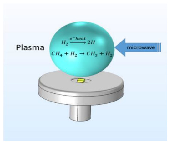
Figure 6.
Schematic diagram of synthetic diamond grown by plasma chemical vapor deposition (MPCVD).
Therefore, the deposition temperature of the substrate surface depends on the distance from the surface of the substrate crystal to the plasma. Because the plasma is spherical, the center of the plasma ball is closer to the surface of the substrate crystal; that is, the temperature of the surface of the substrate crystal is highest near the center of the plasma ball and lower near the periphery of the plasma ball.
There are two ways to change the temperature gradient of the substrate surface: One way is to change the growth temperature of the substrate surface, and the other way is to change the distance between diamond and plasma. Figure 7 shows the surface temperature distribution over the substrate. The temperature gradient on the surface was 40 °C/mm at 1100 °C. Wang [20] reports that the temperature gradient increases with increasing growth temperature, which in turn increases the thermal stress, causing the SCD basal plane to bend. Higher temperatures lead to more severe base plane bending.
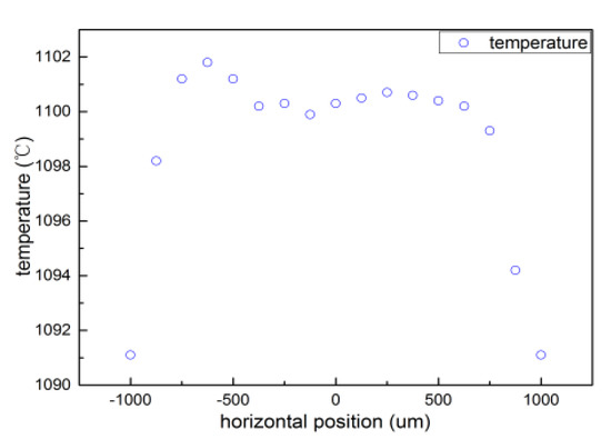
Figure 7.
Distribution of sample surface temperature at 1100 °C.
Figure 8 illustrates the bending model of the basal plane at different growth temperatures. The substrate holders could also play an important role in the deposition of SCD [26,27].
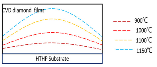
Figure 8.
Results of proposed basal plane bending model for different growth temperatures.
Figure 9 shows the pocket holder design. In this design, the holder height d significantly affects the temperature gradient of the sample surface. Figure 10 shows the temperature gradient as a function of position on the substrate surface and for different holder heights. The results show that, for d = 1.3 mm, the temperature gradient at the surface of the substrate fluctuates significantly. As the thickness of the CVD diamond film increases with growth time, the SCD surface approaches the plasma, and the fluctuations in surface temperature increase. In other words, the internal stress increases, which increases the SCD basal plane bending.
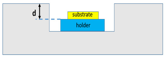
Figure 9.
Pocket holder design for single-crystal diamond (SCD) synthesis.
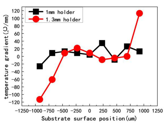
Figure 10.
Temperature gradient as function of substrate surface positions for different holder heights.
4. Conclusions
To summarize, the substrate is the dominant factor for determining the basal plane bending in SCD. An effective method to alleviate basal plane bending is to use high-quality substrates with flat basal planes.
Growth temperature also strongly affects basal plane bending in SCD. A higher growth temperature increases the temperature gradient at the sample surface, which bends the basal plane. When the growth temperatures are 900 °C and 1150 °C, the radius of curvature of the lattice plane of CVD-grown diamond are 358.17 and 23.40 m, respectively. Increasing growth time also leads to more severe basal plane bending. For a growth time of 16 h, the radius of curvature of the lattice plane is 10.20 m.
Finally, increasing the temperature gradient at the sample surface also increases basal plane bending. To describe this phenomenon, we propose that the spherical distribution of the plasma and the distance between the plasma ball and the SCD surface are the main causes for basal plane bending in SCD.
Author Contributions
Conceptualization, X.H. (Xiaotong Han) and P.D.; methodology, X.X. (Xuejian Xie); software, X.W.; validation, Y.P., X.H. (Xiaobo Hu) and X.X. (Xiangang Xu); formal analysis, X.H. (Xiaotong Han); investigation, X.H. (Xiufei Hu); resources, D.W.; data curation, J.Y.; writing—original draft preparation, X.H. (Xiaotong Han); writing—review and editing, Y.P.; visualization, X.H. (Xiaobo Hu); supervision, X.X. (Xiangang Xu); project administration, Y.P.; funding acquisition, D.W. All authors have read and agreed to the published version of the manuscript.
Funding
This work was supported by the National Key R&D Program of China (Grant No. 2018YFB0406501), the Province Key R&D Program of Shandong (Grants No. 2019JZZY010210, No. 2016ZDJS01B03 and No. 2017CXGC0412), Shandong Research Institute of Industrial Technology (Grants No. OX2X2019012).
Acknowledgments
We would like to thank Jinan Diamond Technology Co. Ltd for providing the HPHT diamond substrate that was used in the experiments.
Conflicts of Interest
There are no conflicts of interest to declare.
References
- Gurbuz, Y.; Esame, O.; Tekin, I.; Kang, W.P.; Davidson, J.L. Diamond semiconductor technology for RF device applications. Solid State Electron. 2005, 49, 1055–1070. [Google Scholar] [CrossRef]
- Baliga, B.J. Semiconductors for high-voltage, vertical channel field-effect transistors. J. Appl. Phys. 1982, 53, 1759–1764. [Google Scholar] [CrossRef]
- Huang, Q. New Unipolar Switching Power Device Figures of Merit. IEEE Electron Device Lett. 2004, 25, 298–301. [Google Scholar] [CrossRef]
- Schreck, M.; Asmussen, J.; Shikata, S.; Arnault, J.-C.; Fujimori, N. Large-area high-quality single crystal diamond. MRS Bull. 2014, 39, 504–510. [Google Scholar] [CrossRef]
- Balmer, R.S.; Brandon, J.R.; Clewes, S.L.; Dhillon, H.K.; Dodson, J.M.; Friel, I.; Inglis, P.N.; Madgwick, T.D.; Markham, M.L.; Mollart, T.P.; et al. Chemical vapour deposition synthetic diamond: Materials, technology and applications. J. Phys. Condens. Matter 2009, 21, 364221. [Google Scholar] [CrossRef] [PubMed]
- Khmelnitskiy, R.A. Prospects for the synthesis of large single-crystal diamonds. Phys. Uspekhi 2015, 58, 134–149. [Google Scholar] [CrossRef]
- Panizza, M.; Resini, C.; Raccoli, F.; Busca, G.; Catani, R.; Rossini, S. Oxidation of ethane over vanadia-alumina-based catalysts: Co-feed and redox experiments. Chem. Eng. J. 2003, 93, 181–189. [Google Scholar] [CrossRef]
- Willander, M.; Friesel, M.; Wahab, Q.U.; Straumal, B. Silicon carbide and diamond for high temperature device applications. J. Mater. Sci. Mater. Electron. 2006, 17, 1–25. [Google Scholar] [CrossRef]
- Charris, A.; Nad, S.; Asmussen, J. Exploring constant substrate temperature and constant high pressure SCD growth using variable pocket holder depths. Diam. Relat. Mater. 2017, 76, 58–67. [Google Scholar] [CrossRef]
- Yamada, H.; Chayahara, A.; Mokuno, Y.; Kato, Y.; Shikata, S. A 2-in. mosaic wafer made of a single-crystal diamond. Appl. Phys. Lett. 2014, 104, 102110. [Google Scholar] [CrossRef]
- Yang, X.; Yu, J.; Chen, X.; Peng, Y.; Hu, X.; Xu, X.; Yang, X.; Song, Y.; Wang, R. Basal plane bending of 4H-SiC single crystals grown by sublimation method with different seed attachment methods. CrystEngComm 2018, 20, 6957–6962. [Google Scholar] [CrossRef]
- Cui, Y.; Hu, X.; Xie, X.; Wang, R.; Xu, X. Spatial variation of lattice plane bending of 4H-SiC substrates. CrystEngComm 2017, 19, 3844–3849. [Google Scholar] [CrossRef]
- Ohtani, N.; Katsuno, M.; Fujimoto, T.; Nakabayashi, M.; Tsuge, H.; Yashiro, H.; Ohashi, W. Analysis of Basal Plane Bending and Basal Plane Dislocations in 4H-SiC Single Crystals. Jpn. J. Appl. Phys. 2009, 48, 065503. [Google Scholar] [CrossRef]
- Lee, J.; Skowronski, M.; Sanchez, E.; Chung, G. Origin of basal plane bending in hexagonal silicon carbide single crystals. J. Cryst. Growth 2008, 310, 4126–4131. [Google Scholar] [CrossRef]
- Hock, R.; Konias, K.; Perdicaro, L.; Magerl, A.; Hens, P.; Wellmann, P.J. Observation of Lattice Plane Bending during SiC PVT Bulk Growth Using In Situ High Energy X-Ray Diffraction Materials Science Forum; Trans Tech Publications: Strafa Zurich, Switzerland, 2010; Volume 645, pp. 29–32. [Google Scholar]
- Sumathi, R.R.; Barz, R.U.; Gigler, A.M.; Straubinger, T.; Gille, P. Growth of AlN bulk single crystals on 4H-SiC substrates and analyses of their structural quality and growth mode evolution. Phys. Status Solidi 2012, 209, 415–418. [Google Scholar] [CrossRef]
- Seitz, C.; Herro, Z.G.; Epelbaum, B.M.; Hock, R.; Magerl, A. Lattice-plane curvature and small-angle grain boundaries in SiC bulk crystals. J. Appl. Crystallogr. 2006, 39, 17–23. [Google Scholar] [CrossRef]
- Xie, X.; Wang, X.; Peng, Y.; Cui, Y.; Chen, X.; Hu, X.; Xu, X.; Yu, P.; Wang, R. Synthesis and characterization of high quality {100} diamond single crystal. J. Mater. Sci. Mater. Electron. 2017, 28, 9813–9819. [Google Scholar] [CrossRef]
- Yoganathan, M.; Emorhokpor, E.; Kerr, T.; Gupta, A.; Tanner, C.; Zwieback, I. Characterization of SiC Substrates Using X-Ray Rocking Curve Mapping. Mater. Sci. Forum 2006, 527, 729–732. [Google Scholar] [CrossRef]
- Wang, X.; Duan, P.; Cao, Z.; Liu, C.; Wang, D.; Peng, Y.; Hu, X. Homoepitaxy Growth of Single Crystal Diamond under 300 torr Pressure in the MPCVD System. Materials 2019, 12, 3953. [Google Scholar] [CrossRef]
- Ha, S.Y.; Rohrer, G.S.; Skowronski, M.; Heydemann, V.; Snyder, D.W. Plastic Deformation and Residual Stresses in SiC Boules Grown by PVT. Mater. Sci. Forum 2000, 338–342, 67–70. [Google Scholar] [CrossRef]
- Harris, S.J.; Goodwin, D.G. Growth on the reconstructed diamond (100) surface. J. Phys. Chem. 1993, 97, 23–28. [Google Scholar] [CrossRef]
- Goodwin, D.G. Scaling laws for diamond chemical-vapor deposition. I. Diamond surface chemistry. J. Appl. Phys. 1993, 74, 6888–6894. [Google Scholar] [CrossRef]
- Goodwin, D.G.; Butler, J.E. Theory of Diamond Chemical Vapor Deposition; Marcel Dekker, Inc.: New York, NY, USA, 2018; pp. 527–581. [Google Scholar]
- Silva, F.; Achard, J.; Brinza, O.; Bonnin, X.; Hassouni, K.; Anthonis, A.; De Corte, K.; Barjon, J. High quality, large surface area, homoepitaxial MPACVD diamond growth. Diam. Relat. Mater. 2009, 18, 683–697. [Google Scholar] [CrossRef]
- Nad, S.; Gu, Y.; Asmussen, J. Growth strategies for large and high quality single crystal diamond substrates. Diam. Relat. Mater. 2015, 60, 26–34. [Google Scholar] [CrossRef]
- Mokuno, Y.; Chayahara, A.; Soda, Y.; Horino, Y.; Fujimori, N. Synthesizing single-crystal diamond by repetition of high rate homoepitaxial growth by microwave plasma CVD. Diam. Relat. Mater. 2005, 14, 1743–1746. [Google Scholar] [CrossRef]
© 2020 by the authors. Licensee MDPI, Basel, Switzerland. This article is an open access article distributed under the terms and conditions of the Creative Commons Attribution (CC BY) license (http://creativecommons.org/licenses/by/4.0/).