Abstract
We investigated the flash light sintering process to effectively reduce electrical resistance in silver nanowire networks. The optimum condition of the flash light sintering process reduces the electrical resistance by ~20%, while the effect of the conventional thermal annealing processes is rather limited for silver nanowire networks. After flash light sintering, the morphology of the junction between the silver nanowires changes to a mixed-phase structure of the two individual nanowires. This facile and fast process for silver nanowire welding could be highly advantageous to the mass production of silver nanowire networks.
1. Introduction
Transparent conductive electrodes (TCE) are considered one of the most important technologies for developing next generation electronic devices including liquid crystal displays, light emitting diodes, touch screens, and photovoltaic cells [1,2,3,4]. Research in the field of TCE is dedicated to the development of state-of-the-art technology that can combine high electrical conductivity with comparable optical transmittance in large-area devices [5]. Additionally, researchers have focused on introducing the flexibility of TCE components to the manufacturing of foldable/rollable electronic devices. So far, the indium tin oxide (ITO) is the most widely used material in TCE because of its high electrical conductivity and transmittance properties [6]. Much effort has been devoted to realizing flexible ITO by reducing the thickness of the conducting layer. However, the intrinsic brittleness of the oxide materials cannot withstand severe deformation, such as the 1 mm-radius bending stress necessary for foldable devices [7].
Metal nanowires (NWs), which are one-dimensional metal structures with high aspect ratio, have been proposed as the ideal material for flexible TCE due to their high electrical conductivity with low surface coverage [8,9,10,11,12,13]. Networks of NWs are highly advantageous to the industry because they can be used to produce large-area films by implementing simple coating techniques (e.g., slot-die coating, which is a common method in film-producing). Much research has been conducted to overcome the trade-off relation of electrical conductivity/transmittance in NW networks [14]. It has been demonstrated that longer metallic NWs could lead to positive effects on the electrical conductivity-transmittance relation [15]. The lengths of as-synthesized NWs are typically around several micrometres. Furthermore, silver (Ag) is considered to be the most promising material with respect to realising the feasibility of NW networks [16,17,18]. Devices containing Ag NWs have attracted much interest owing to their low-dimensional structure, which can lead to enhanced transparency and electric conductivity for applications in transparent conducting electrodes [19]. However, the insulating ligands used for Ag NW synthesis are typically made of polyvinylpyrrolidone (PVP), and the solution dispersion process can reduce electrical conductivity because of the large contact resistance between NWs [20]. Therefore, an additional fabrication process is required to reduce junction resistance between Ag NWs to optimize network conductivity.
Many methods for welding NWs have been reported, such as mechanical pressing, Joule heating, thermal sintering, electron beam-induced welding, plasmonic welding, soldering, and focused ion-beam welding [21,22,23,24,25,26]. Among them, thermal sintering, e.g., in ovens and furnaces, has been predominantly used for the sintering of NWs because it is a facile and cost-effective process. However, thermal sintering has serious drawbacks, i.e., low heating and cooling rates and long processing times. Various reports from experimental and theoretical approaches have showed that nanowire structures can easily change into nanoparticles at elevated temperatures at which the Ag atoms move easily by diffusion; a phenomenon known as Rayleigh instability [27,28,29]. To protect NW-welding from over-diffusion and breaking, precise control of the applied energy is necessary. The process of optical heating is considered suitable for welding because of its short irradiation time. While optical heating has several advantages over thermal processes, the morphological transformation of nanowires under light irradiation has been scarcely investigated [30,31]. In this study, we attempted to construct Ag NW networks via the flash light sintering process, which can selectively sinter the junction of Ag NW networks to effectively reduce electrical conductivity. Additionally, we performed a detailed analysis on the junction structure after flash light sintering to understand the mechanism behind Ag NW welding. The flash light sintering process could be an easy and cost-effective way to integrate Ag NWs into TCE devices.
2. Materials and Methods
Ag NWs were synthesized using a modified polyol process, as previously reported. First, 6 g of PVP was slowly added to 70 mL of ethylene glycol (EG) and completely dissolved at 60 °C. After a clear solution was formed, 2 g of AgNO3 was added and dissolved within 15 min. Then, an FeCl3 solution (0.05 M, 100 μL) was added into the mixture solution at room temperature, and the solution was placed in a pre-heated reactor to grow Ag NWs at 150 °C for 60 min. Finally, the suspension was cooled to 60 °C, and acetone and ethanol were used to wash the precipitate three times by centrifugation at 5000 rpm for 10 min.
Ag NWs were re-dispersed in ethanol and coated on an SiO2/Si substrate using the air spray method. The size of SiO2/Si substrate is 3 cm × 1 cm and the size of Ag NWs network is around 1 cm × 0.8 cm. Air pressure and needle-to-substrate distance were critical parameters for the spray coating process to ensure a uniform Ag NW network. To measure the electrical resistance, we made the electrodes on end of the prepared Ag NWs network by Ag paste. Consequently, the Ag NW networks were treated with a white light flash from a xenon lamp (ILC technology, L6755, Sunnyvale, CA, USA) comprising a wavelength range of 230–1600 nm and using a variable irradiation time. The pulse duration ranged from 1 to 5 ms, and quartz was used as a light guide. The size of spot was more than 1 cm × 1 cm, which could cover the whole Ag NW networks. The flash light was also applied on the Ag electrodes, but there was no change for Ag electrodes.
The electrical resistance of the Ag NW networks was measured using a conventional multimeter. The microstructure was investigated using scanning electron microscopy (SEM) (JSM-7600F, JEOL, Tokyo, Japan) and transmission electron microscopy (TEM) (JEM-2100F, JEOL, Tokyo, Japan).
3. Results and Discussion
The sintering process for the Ag NW network is schematically illustrated in Figure 1. When the external energy, e.g., thermal heating or optical irradiation, is applied to the nanowire junction, a mass diffusion causes the morphology to change. At the first stage, the PVP layers between Ag NW junctions are eliminated owing to the low melting temperature of the material. When two nanowires come into contact, junction welding starts to minimize its surface energy. As further external energy is applied, the Ag NWs begin to break and transform to completely fragmented particles. However, typical annealing process can give the Ag NWs welding and breaking together (shown on Figure 1a) due to its high applied energy; thus, the heat treatment duration is expected to be a critical factor for determining the Ag NW weld quality and enhancing the electrical conductivity of NW networks. The short process time of flash light sintering potentially makes it a superior process for providing sufficient external energy when constructing Ag NW networks (Figure 1b).
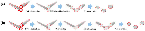
Figure 1.
Schematic diagram of the morphology transformation of Ag nanowire (NW) under (a) thermal heating or high flash light sintering; (b) optimal condition of flash light sintering.
Figure 2a presents the change in electrical resistance of Ag NW networks during thermal heating at a 5 °C/min ramp rate at a temperature up to 240 °C. The relative resistance, R/R0, increases monotonically at first and abruptly when the temperature reaches 200 °C. To investigate the morphology changes in terms of the applied temperature, Ag NWs deposited on SiO2/Si substrates were annealed isothermally at 130, 170, and 200 °C for 10 min. SEM images of the thermal heating process at the selected temperature are displayed in Figure 2. Ag NW networks annealed at 130 and 170 °C did not show any morphological change, as shown in Figure 2a–d. However, after annealing at 200 °C, the majority of the wires broke into isolated short wires or particles, leading to a significant enhancement of the electrical resistance (Figure 2a).
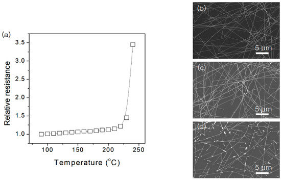
Figure 2.
(a) Variation of the electrical resistance of Ag NW network during thermal annealing in air running from room temperature to 240 °C with a heating ramp rate of 5 °C/min. Morphologies of the Ag NWs after the 10-min heat treatment at (b) 130 °C, (c) 170 °C, and (d) 200 °C.
To evaluate the electrical resistance change of the Ag NW network in terms of the flash light sintering process conditions, we deposited the Ag NW network on the Si/SiO2 substrate and added the Ag paste on the ends of substrate for tracking the electrical resistance change by the flash light applying conditions, as shown in Figure 3a. The samples were prepared depending on the irradiation energy, duration time, and number of irradiations. At the relatively low irradiation energy density of 1.02 J/cm2, a reduced electrical resistance was observed at the samples under a duration time of 2 ms (Figure 3b). At the lowest irradiation energy density, 1 ms of irradiation was not enough for the formation of welded connections between Ag NWs. Moreover, a relatively high electrical resistance was introduced even after repeated irradiation. For longer duration times, the electrical resistance was decreased by inter-connected Ag NWs, but some Ag NWs hindered electrical conductivity. It was also observed that the highly increased electrical resistance originated from further fragmentation of NWs by repeated irradiation. For a moderate duration time of 2 ms, the electrical resistance significantly decreases to ~80% of the original electrical resistance, indicating that this duration time is the optimum duration time for the formation of well-connected NWs. At the highest irradiation energy density of 1.54 J/cm2, the decrease in electrical resistance is limited and saturated by the combined effects of inter-connected junctions and NWs breaking (Figure 3c). For high irradiation energy densities and long duration times, the formation of isolated NWs is intensified, corresponding to an increased electrical resistance for repeated irradiation. It should be noted that the electrical conductivity of Ag NW networks can be enhanced by optimizing the irradiation energy and duration time during the flash light sintering process.
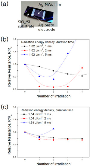
Figure 3.
(a) Photograph of an Ag NW network deposited on a Si/SiO2 substrate. Variation of the electrical resistance of the Ag NW network during repeated flash light irradiation as a function of the number of irradiations for an energy density of (b) 1.02 J/cm2 and (c) 1.54 J/cm2 in air at room temperature.
To support the relationship between the electrical conductivity and morphological changes of the NW network during irradiation, an SEM analysis of the samples with respect to the duration time was conducted, as shown in Figure 4. At a duration time of 1 ms under an irradiation energy density of 1.02 J/cm2, the welding process of Ag NWs is not completed because of insufficient irradiation time. This implies that a high electrical resistance remains after repeated irradiation under the 1 ms-1.02 J/cm2 condition (Figure 3b). We have already confirmed from the electrical conductivity measurement that the optimum condition of flash light sintering corresponds to an irradiation energy density of 1.02 J/cm2 and an irradiation time of 2 ms. Under this condition, we cannot directly distinguish the difference between the SEM images of 1 ms and 2 ms (Figure 4a,b), but the morphology of welded structure will be discussed on the TEM analysis section. Under the 5 ms-1.02 J/cm2 condition, the Ag NWs are broken and electrical resistance is significantly increased. We conclude that the trend in morphological changes of Ag NWs as a function of the applied energy during the flash light sintering process is consistent with the trend in the electrical resistance of Ag NW networks.
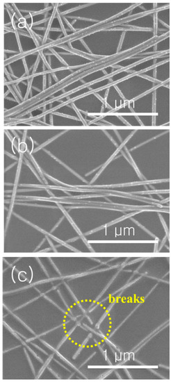
Figure 4.
SEM images of Ag NW networks after irradiation under an irradiation energy density of 1.02 J/cm2 and a duration time of (a) 1 ms, (b) 2 ms, and (c) 5 ms.
When a Ag NW network is directly exposed to ambient conditions, atmospheric sulfur such as hydrogen sulfide (H2S) or carbonyl sulfide (OCS) can easily react with the intrinsic defect structure of the Ag NW pentagon, which leads to a significant increase in electrical resistance. [32,33,34,35,36] This is one of the most important issues with Ag NW networks for practical applications. We also track the electrical resistance of the Ag NW network in terms of days of exposure. Figure 5a shows the SEM images after 10 days of exposure to ambient conditions. We can easily find nanoparticles that exhibit a typical morphological feature of Ag NW sulfidation. Compared to other reports [37,38], our flash light-sintered Ag NWs show a relatively low increase in relative resistance without any protection layer (see Figure 5b), which is caused by the removal of the strain on the junction of the Ag NW network. The 1.5-fold increase in electrical resistance could also give a significant problem for expanding the applications, which should be considered on other researches.
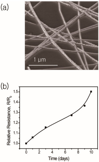
Figure 5.
(a) SEM image of the Ag NW network by sulfidation and (b) the change in relative electrical resistance of the Ag NW network after 10-day exposure to air.
A TEM analysis has been conducted for obtaining the junction structure before/after the flash light welding process. Figure 6a shows the two inter-connected Ag NWs after the coating process. Each Ag NW remains an individual structure, and the pentagonal structure of [111] direction of the Ag NWs is clearly observed [39]. Under the optimum condition (1.02 J/cm2, 2 ms) of the flash light sintering process, the junction structure is completely changed to the mixed-phase structure of two Ag NWs. The selected area electron diffraction (SAED) pattern of the welded Ag NWs has two different indices, i.e., [111] and [110], which correspond to the parallel and perpendicular direction of Ag NWs growth (Figure 6c). While the upper Ag NW morphology assumes an amorphous structure, the structure remains identical to the individual Ag NWs. Figure 6d shows a schematic diagram of the direction of the welded Ag NWs that supports crossing and networking. The optimal flash sintering is suitable for fabricating Ag NW networks that have low contact and electrical resistance.
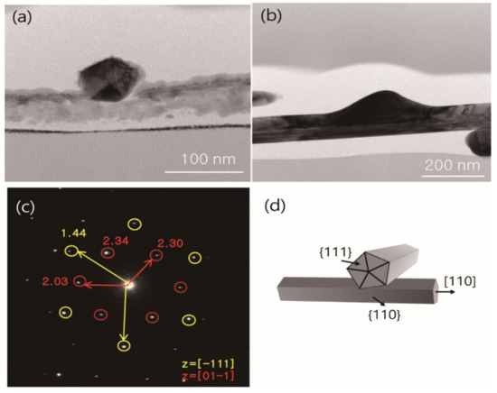
Figure 6.
TEM images of Ag NWs (a) before and (b) after the flash light sintering process; (c) selected area electron diffraction (SAED) pattern of the junction of welded Ag NWs; (d) schematic diagram of two welded nanowires.
4. Conclusions
In summary, we performed the flash light sintering process to investigate the welding mechanism of Ag NW networks to effectively reduce the electrical resistance. The optimised condition of the flash light sintering process could reduce the electrical resistance by ~20%, more stable than other papers [37,38] without any protection layer. After flash light sintering, the junction structure of the Ag NWs changed to the welded structure which was identical to the original Ag NW crystal structures significantly reducing the electrical resistance. Furthermore, with this process, a wielded structure with low electrical resistance can be obtained rapidly. Therefore, this technique could be applied to the mass production of Ag NW networks for transparent electrode areas.
Author Contributions
D.-J.Y. and W.H.S. (Weon Ho Shin) designed the experiments. S.K., W.H.S. (Woo Hyeong Sim), and H.M.J. performed the experiments. H.S. and K.-S.M. analysed the samples. All the authors discussed the data and wrote the manuscript. All authors have read and agreed to the published version of the manuscript
Funding
This research was supported by the Basic Science Research Program of the National Research Foundation of Korea (NRF), funded by the Ministry of Science and ICT (NRF-2018R1C1B6004358, NRF-2017R1D1A1B03034322, NRF-2018R1C1B5033164). This study was supported by 2018 Research Grant (PoINT) from Kangwon National University.
Conflicts of Interest
The authors declare no conflict of interest.
References
- Granqvist, C.G. Transparent conductive electrodes for electrochromic devices: A review. Appl. Phys. 1993, 57, 19–24. [Google Scholar] [CrossRef]
- Jiang, X.; Wong, F.L.; Fung, M.K.; Lee, S.T. Aluminum-doped zinc oxide films as transparent conductive electrode for organic light-emitting devices. Appl. Phys. Lett. 2003, 83, 1875–1877. [Google Scholar] [CrossRef]
- Liu, H.; Avrutin, V.; Izyumskaya, N.; Özgür, Ü.; Morkoç, H. Transparent conducting oxides for electrode applications in light emitting and absorbing devices. Superlattices Microstruct. 2010, 48, 458–484. [Google Scholar] [CrossRef]
- Ricciardulli, A.G.; Yang, S.; Wetzelaer, G.-J.A.H.; Feng, X.; Blom, P.W.M. Hybrid Silver Nanowire and Graphene-Based Solution-Processed Transparent Electrode for Organic Optoelectronics. Adv. Funct. Mater. 2018, 28. [Google Scholar] [CrossRef]
- Kuang, P.; Park, J.-M.; Leung, W.; Mahadevapuram, R.C.; Nalwa, K.S.; Kim, T.-G.; Chaudhary, S.; Ho, K.-M.; Constant, K. A New Architecture for Transparent Electrodes: Relieving the Trade-Off Between Electrical Conductivity and Optical Transmittance. Adv. Mater. 2011, 23, 2469–2473. [Google Scholar] [CrossRef]
- Minami, T. Substitution of transparent conducting oxide thin films for indium tin oxide transparent electrode applications. Thin Solid Film. 2008, 516, 1314–1321. [Google Scholar] [CrossRef]
- Alzoubi, K.; Hamasha, M.M.; Lu, S.; Sammakia, B. Bending Fatigue Study of Sputtered ITO on Flexible Substrate. J. Disp. Technol. 2011, 7, 593–600. [Google Scholar] [CrossRef]
- Hu, L.; Wu, H.; Cui, Y. Metal nanogrids, nanowires, and nanofibers for transparent electrodes. MRS Bull. 2011, 36, 760–765. [Google Scholar] [CrossRef]
- Guo, H.; Lin, N.; Chen, Y.; Wang, Z.; Xie, Q.; Zheng, T.; Gao, N.; Li, S.; Kang, J.; Cai, D.; et al. Copper Nanowires as Fully Transparent Conductive Electrodes. Sci. Rep. 2013, 3, 2323. [Google Scholar] [CrossRef] [PubMed]
- Jeong, I.; Lee, J.; Josepha, K.L.V.; Lee, H.I.; Kim, J.K.; Yoon, S.; Lee, J. Low-cost electrospun WC/C composite nanofiber as a powerful platinum-free counter electrode for dye sensitized solar cell. Nano Energy 2014, 9, 392–400. [Google Scholar] [CrossRef]
- Sohn, H.; Park, C.; Oh, J.-M.; Kang, S.W.; Kim, M.-J. Silver Nanowire Networks: Mechano-Electric Properties and Applications. Materials 2019, 12, 2526. [Google Scholar] [CrossRef] [PubMed]
- Sohn, H.; Kim, S.Y.; Shin, W.; Lee, J.M.; Moon, K.-S.; Lee, H.; Yun, D.-J.; Han, I.T.; Kwak, C.; Hwang, S.-J. Novel Flexible Transparent Conductive Films with Enhanced Chemical and Electro-Mechanical Sustainability: TiO2 Nanosheet-Ag Nanowire Hybrid. ACS Appl. Mater. Interfaces 2018, 10, 2688–2700. [Google Scholar] [CrossRef] [PubMed]
- Sohn, H.; Woo, Y.S.; Shin, W.-H.; Yun, D.-J.; Lee, T.; Kim, F.S.; Hwang, J. Novel Transparent Conductor with Enhanced Conductivity: Hybrid of Silver Nanowires and Dual-Doped Graphene. Appl. Surf. Sci. 2017, 419, 63–69. [Google Scholar] [CrossRef]
- van de Groep, J.; Spinelli, P.; Polman, A. Transparent Conducting Silver Nanowire Networks. Nano Lett. 2012, 12, 3138–3144. [Google Scholar] [CrossRef]
- Lee, J.-Y.; Connor, S.T.; Cui, Y.; Peumans, P. Solution-Processed Metal Nanowire Mesh Transparent Electrodes. Nano Lett. 2008, 8, 689–692. [Google Scholar] [CrossRef]
- Lim, J.-W.; Cho, D.-Y.; Jihoon, K.; Na, S.-I.; Kim, H.-K. Simple brush-painting of flexible and transparent Ag nanowire network electrodes as an alternative ITO anode for cost-efficient flexible organic solar cells. Sol. Energy Mater. Sol. Cells 2012, 107, 348–354. [Google Scholar] [CrossRef]
- De, S.; Higgins, T.M.; Lyons, P.E.; Doherty, E.M.; Nirmalraj, P.N.; Blau, W.J.; Boland, J.J.; Coleman, J.N. Silver Nanowire Networks as Flexible, Transparent, Conducting Films: Extremely High DC to Optical Conductivity Ratios. ACS Nano 2009, 3, 1767–1774. [Google Scholar] [CrossRef]
- Bellew, A.T.; Manning, H.G.; Gomes da Rocha, C.; Ferreira, M.S.; Boland, J.J. Resistance of Single Ag Nanowire Junctions and Their Role in the Conductivity of Nanowire Networks. ACS Nano 2015, 9, 11422–11429. [Google Scholar] [CrossRef]
- Lee, J.; Lee, P.; Lee, H.; Lee, D.; Lee, S.S.; Ko, S.H. Very long Ag nanowire synthesis and its application in a highly transparent, conductive and flexible metal electrode touch panel. Nanoscale 2012, 4, 6408–6414. [Google Scholar] [CrossRef]
- Hwang, J.; Shim, Y.; Yoon, S.-M.; Lee, S.H.; Park, S.-H. Influence of polyvinylpyrrolidone (PVP) capping layer on silver nanowire networks: Theoretical and experimental studies. RSC Adv. 2016, 6, 30972–30977. [Google Scholar] [CrossRef]
- Lee, J.; Lee, I.; Kim, T.-S.; Lee, J.-Y. Efficient Welding of Silver Nanowire Networks without Post-Processing. Small 2013, 9, 2887–2894. [Google Scholar] [CrossRef] [PubMed]
- Xu, S.; Tian, M.; Wang, J.; Xu, J.; Redwing, J.M.; Chan, M.H.W. Nanometer-Scale Modification and Welding of Silicon and Metallic Nanowires with a High-Intensity Electron Beam. Small 2005, 1, 1221–1229. [Google Scholar] [CrossRef] [PubMed]
- Han, S.; Hong, S.; Ham, J.; Yeo, J.; Lee, J.; Kang, B.; Lee, P.; Kwon, J.; Lee, S.S.; Yang, M.-Y.; et al. Fast Plasmonic Laser Nanowelding for a Cu-Nanowire Percolation Network for Flexible Transparent Conductors and Stretchable Electronics. Adv. Mater. 2014, 26, 5808–5814. [Google Scholar] [CrossRef] [PubMed]
- Liang, J.; Li, L.; Tong, K.; Ren, Z.; Hu, W.; Niu, X.; Chen, Y.; Pei, Q. Silver Nanowire Percolation Network Soldered with Graphene Oxide at Room Temperature and Its Application for Fully Stretchable Polymer Light-Emitting Diodes. ACS Nano 2014, 8, 1590–1600. [Google Scholar] [CrossRef] [PubMed]
- Song, T.-B.; Chen, Y.; Chung, C.-H.; Yang, Y.; Bob, B.; Duan, H.-S.; Li, G.; Tu, K.-N.; Huang, Y.; Yang, Y. Nanoscale Joule Heating and Electromigration Enhanced Ripening of Silver Nanowire Contacts. ACS Nano 2014, 8, 2804–2811. [Google Scholar] [CrossRef]
- Kang, H.; Song, S.-J.; Sul, Y.E.; An, B.-S.; Yin, Z.; Choi, Y.; Pu, L.; Yang, C.-W.; Kim, Y.S.; Cho, S.M.; et al. Epitaxial-Growth-Induced Junction Welding of Silver Nanowire Network Electrodes. ACS Nano 2018, 12, 4894–4902. [Google Scholar] [CrossRef]
- Mead-Hunter, R.; King, A.J.C.; Mullins, B.J. Plateau Rayleigh Instability Simulation. Langmuir 2012, 28, 6731–6735. [Google Scholar] [CrossRef]
- Gill, S.P.A. Controlling the Rayleigh instability of nanowires. Appl. Phys. Lett. 2013, 102, 143108. [Google Scholar] [CrossRef]
- Karim, S.; Toimil-Molares, M.E.; Ensinger, W.; Balogh, A.G.; Cornelius, T.W.; Khan, E.U.; Neumann, R. Influence of crystallinity on the Rayleigh instability of gold nanowires. J. Phys. Appl. Phys. 2007, 40, 3767–3770. [Google Scholar] [CrossRef]
- Garnett, E.C.; Cai, W.; Cha, J.J.; Mahmood, F.; Connor, S.T.; Greyson Christoforo, M.; Cui, Y.; McGehee, M.D.; Brongersma, M.L. Self-limited plasmonic welding of silver nanowire junctions. Nat. Mater. 2012, 11, 241–249. [Google Scholar] [CrossRef]
- Oh, H.; Lee, J.; Lee, M. Transformation of silver nanowires into nanoparticles by Rayleigh instability: Comparison between laser irradiation and heat treatment. Appl. Surf. Sci. 2018, 427, 65–73. [Google Scholar] [CrossRef]
- Keast, V.J.; Myles, T.A.; Shahcheraghi, N.; Cortie, M.B. Corrosion processes of triangular silver nanoparticles compared to bulk silver. J. Nanoparticle Res. 2016, 18, 45–56. [Google Scholar] [CrossRef]
- Wang, X.; Santshi, C.; Martin, O. Strong improvement of long-term chemical and thermal stability of plasmonic silver nanoantennas and films. Small 2017, 13. [Google Scholar] [CrossRef] [PubMed]
- Kang, H.; Buchman, J.T.; Rodriguez, R.S.; Ring, H.T.; He, J.; Bantz, K.C.; Haynes, C.L. Stabilization of silver and gold nanoparticles: Preservation and improvement of plasmonic functionalities. Chem. Rev. 2019, 119, 664–699. [Google Scholar] [CrossRef] [PubMed]
- Madeira, A.; Plissonneau, M.; Servant, L.; Goldthorpe, I.A.; Tréguer-Delapierre, M. Increasing Silver Nanowire Network Stability through Small Molecule Passivation. Nanomaterials 2019, 9, 899. [Google Scholar] [CrossRef] [PubMed]
- Elechiguerra, J.L.; Larios-Lopez, L.; Liu, C.; Garcia-Gutierrez, D.; Camacho-Bragado, A.; Yacaman, M.J. Corrosion at the Nanoscale: The Case of Silver Nanowires and Nanoparticles. Chem. Mater. 2005, 17, 6042–6052. [Google Scholar] [CrossRef]
- Deignan, G.; Goldthorpe, I.A. The dependence of silver nanowire stability on network composition and processing parameters. RSC Adv. 2017, 7, 35590–35597. [Google Scholar] [CrossRef]
- Lee, E.; Ahn, J.; Kwon, H.C.; Ma, S.; Kim, K.; Yun, S.; Moon, J. All-Solution-Processed Silver Nanowire Window Electrode-Based Flexible Perovskite Solar Cells Enabled with Amorphous Metal Oxide Protection. Adv. Energy Mater. 2018, 8. [Google Scholar] [CrossRef]
- Zhang, P.; Wyman, I.; Hu, J.; Lin, S.; Zhong, Z.; Tu, Y.; Huang, Z.; Wei, Y. Silver nanowires: Synthesis technologies, growth mechanism and multifunctional applications. Mater. Sci. Eng. 2017, 223, 1–23. [Google Scholar] [CrossRef]


© 2020 by the authors. Licensee MDPI, Basel, Switzerland. This article is an open access article distributed under the terms and conditions of the Creative Commons Attribution (CC BY) license (http://creativecommons.org/licenses/by/4.0/).