Article

Low-Temperature In-Induced Holes Formation in Native-SiOx/Si(111) Substrates for Self-Catalyzed MBE Growth of GaAs Nanowires

by
Rodion R. Reznik
1,2,3,4,*,
Konstantin P. Kotlyar
2,
Vladislav O. Gridchin
1,
Evgeniy V. Ubyivovk
1,2,3,
Vladimir V. Federov
1,
Artem I. Khrebtov
3,
Dmitrii S. Shevchuk
1 and
George E. Cirlin
1,3,4,5
1
Alferov University, ul. Khlopina 8/3, 194021 St. Petersburg, Russia
2
Saint-Petersburg State University, Universitetskaya Emb. 13B, 198504 St. Petersburg, Russia
3
ITMO University, Kronverkskiy pr. 49, 197101 St. Petersburg, Russia
4
Institute for Analytical Instrumentation RAS, Rizhsky 26, 190103 St. Petersburg, Russia
5
Saint-Petersburg Electrotechnical University “LETI”, ul. Professora Popova 5, 197376 St. Petersburg, Russia
*
Author to whom correspondence should be addressed.
Materials 2020, 13(16), 3449; https://doi.org/10.3390/ma13163449
Submission received: 26 June 2020 / Revised: 1 August 2020 / Accepted: 3 August 2020 / Published: 5 August 2020
(This article belongs to the Special Issue Electronic Materials and Devices)

Abstract

:
The reduction of substrate temperature is important in view of the integration of III–V materials with a Si platform. Here, we show the way to significantly decrease substrate temperature by introducing a procedure to create nanoscale holes in the native-SiOx layer on Si(111) substrate via In-induced drilling. Using the fabricated template, we successfully grew self-catalyzed GaAs nanowires by molecular-beam epitaxy. Energy-dispersive X-ray analysis reveals no indium atoms inside the nanowires. This unambiguously manifests that the procedure proposed can be used for the growth of ultra-pure GaAs nanowires.

1. Introduction

Nowadays III–V semiconductor nanowires (NWs) attract increasing attention due to recent advances made in their use as building elements for various electronic, optical, and biological applications [1,2,3,4]. Due to their ability to accumulate strain in two dimensions [5,6,7], NWs geometry is ideal for the monolithic integration of semiconductor materials with different lattice-mismatched substrates, which is important for achieving high-performance optoelectronic devices based on Si technology. A commonly used NWs fabrication technique relies on the Au-catalytic mechanism generally referred to as vapor-liquid-solid (VLS) growth [8,9]. However, Au is known to be a detrimental impurity in Si, limiting the integration of those nano-objects with a Si platform [10]. Moreover, the use of Au as a catalyst can lead to uncontrolled doping of III–V NWs [11,12]. On the other hand, successful attempts to grow self-catalyzed GaAs NWs on silicon [13,14,15] are very promising. However, GaAs NWs arrays synthesized on an unprepared Si surface are usually not homogeneous in terms of the height and diameter of NWs, which is critical for many applications. Plissard et al. [16] and Reznik et al. [17] have shown that the use of Si substrates with a SiOx covering layer and electron-beam lithography technique for forming holes in SiOx allows one to synthesize regular and homogeneous arrays of self-catalyzed GaAs NWs on a substrate surface. By changing the size and the distance between holes in SiOx, it is possible to control the morphological parameters of the NWs array, such as the density and the diameter of NWs. The synthesis of regular and homogeneous NWs arrays with controlled morphological properties is necessary for numerous applications. However, the high cost and time-consumption of the electron-beam lithography processes encourage researchers to find other ways to synthesize homogeneous and separated NWs. It was demonstrated in the work of I Morral et al. [18] that gallium adatoms interact with SiO2 forming sparse nanocraters on preexisting subnanometer pinholes. Küpers et al. [19] introduced a two-step growth method, where Ga droplets are pre-deposited on SiOx/Si substrates to form pinholes in SiOx for subsequent NWs synthesis. In order to further improve the homogeneity and controllability of GaAs NWs density and diameters, Tauchnitz et al. [20] developed a three-step in-situ surface modification procedure for non-patterned native-SiOx/Si(111) substrates which decouples the Ga-induced hole formation in SiOx from the following Ga-assisted growth of GaAs NWs. Koivusalo et al. [21] added two more steps to the technology described in [20]: crystallization of Ga droplets into GaAs by As2 exposure and spontaneous oxidation of the Si surface by air exposure outside the MBE setup. But in all these cases, substrate temperature reached 660–780 °C during the procedure before the initiation of NWs MBE growth. However, reduction of the maximum temperature of the NWs growth process is critical for the integration of III–V materials with silicon technology.
Here, we present a novel approach to low-temperature In-induced holes formation in SiOx for GaAs NWs MBE growth. The temperature at which indium adatoms form holes in SiOx and evaporate from the surface is significantly lower than for gallium ones. Moreover, indium droplets do not etch silicon and do not interact with it [22]. The above makes it possible to decrease the substrate preparation temperature to a lower level than typical GaAs NWs MBE growth temperature.

2. Materials and Methods

GaAs NWs were grown on non-patterned native-SiOx/Si(111) substrates using MBE setup Riber Compact 21 equipped with Ga, In effusion cells and a valved cracker source for the supply of As4. Firstly, the substrate was outgassed at 350 °C for 1 h in an ultrahigh vacuum and then transferred into the growth chamber with no vacuum brake. Afterwards, the substrate was heated to a temperature of 400 °C, and after temperature stabilization, the In source shutter was opened for 20 s to form In droplet on the substrate surface. The In flux was set at 0.4 ML/s according to previous calibrations. On the next step the substrate was kept at the same temperature for 15 min for the etching of the holes in SiOx induced by indium droplets. In order to stop the etching of the holes, the In droplets were crystallized into InAs by 2 min As4 exposure. It was established previously that under similar growth conditions InAs nanoscale islands may be grown on Si(100) surface [23,24,25]. After that the substrate was annealed for 5 min at a temperature of 550 °C to evaporate the InAs completely from the substrate surface. In the following step aimed at the growth of the NWs the substrate temperature was increased to 600 °C for Ga deposition on the surface during 5 s with a 15 s pause to enhance Ga adatoms diffusion towards the holes and to form droplets inside them. Finally, GaAs NWs growth was performed under Ga-rich conditions by opening Ga and As shutters for 10 min. The gallium flux was constant throughout the experiment and was set at 1 ML/s according to the previous calibrations.
In order to evaluate the parameters of the holes that were formed in SiOx layer, firstly, only In was deposited with following etching, crystallization, and evaporation. The surface morphology of the native-SiOx/Si substrate with holes after etching was studied using atomic force microscopy (AFM, BioScope Catalyst, Bruker, Santa Barbara, CA, USA). After NWs growth, the morphology of the grown NWs was studied by scanning electron microscopy (SEM, Supra 25, Carl Zeiss, Oberkochen, Germany). Microstructure and chemical composition of the grown NWs were investigated by transmission electron microscopy (TEM, Libra 200FE, Carl Zeiss, Oberkochen, Germany) with energy-dispersive X-ray (EDX) spectroscopy techniques (X-Max 80, Oxford Ins., High Wycombe, UK).

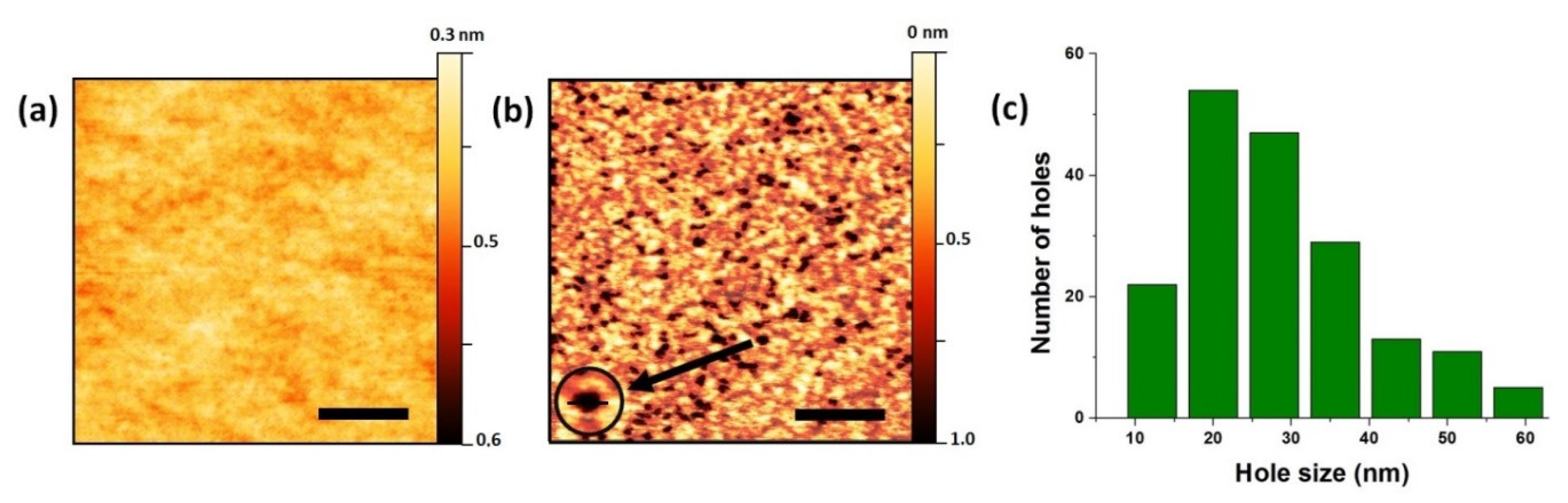
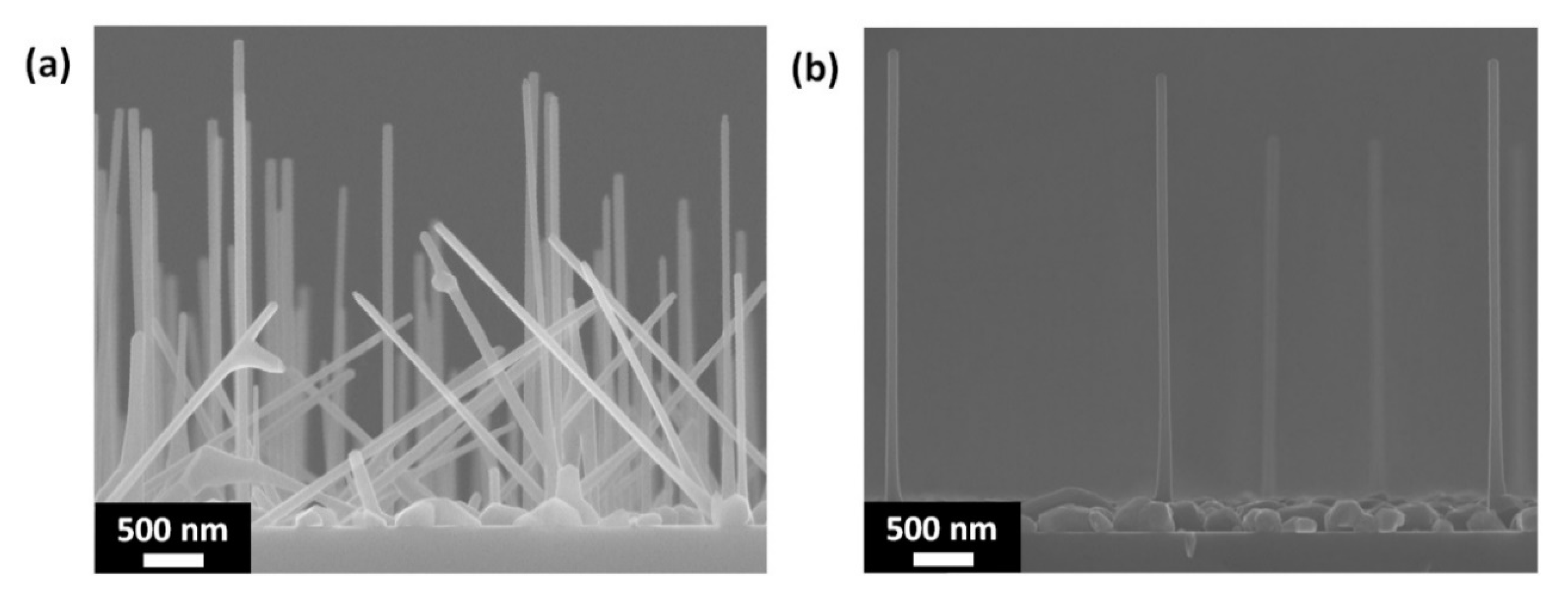
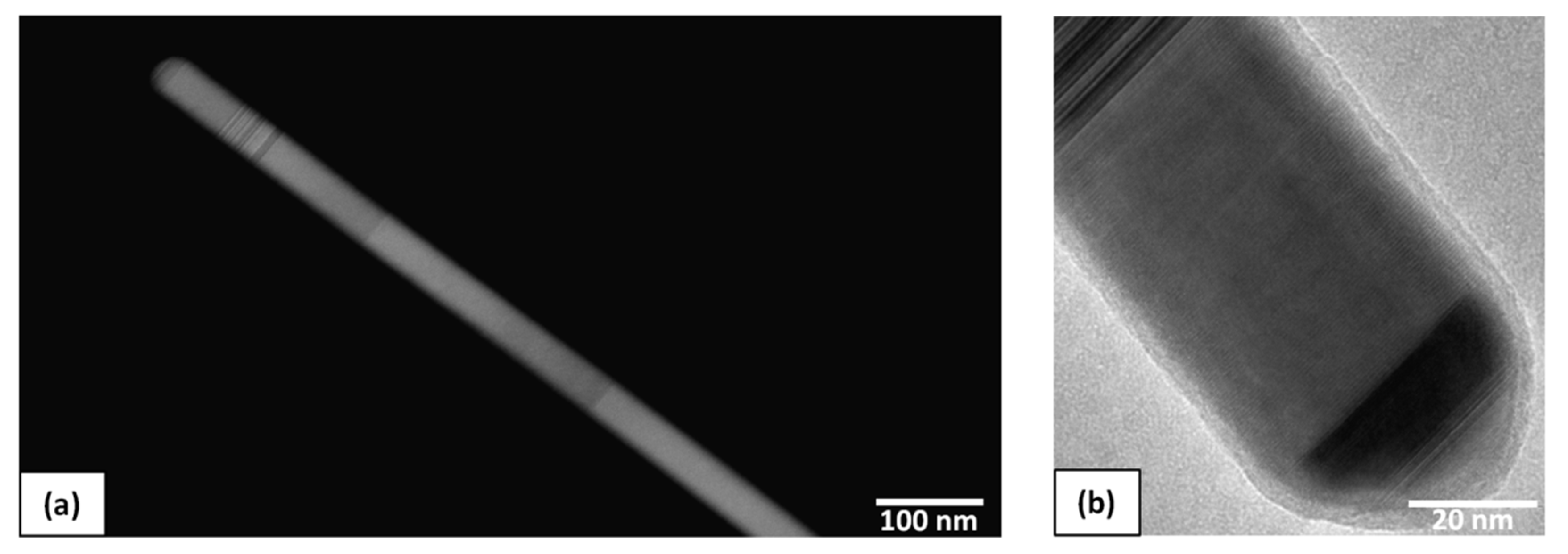
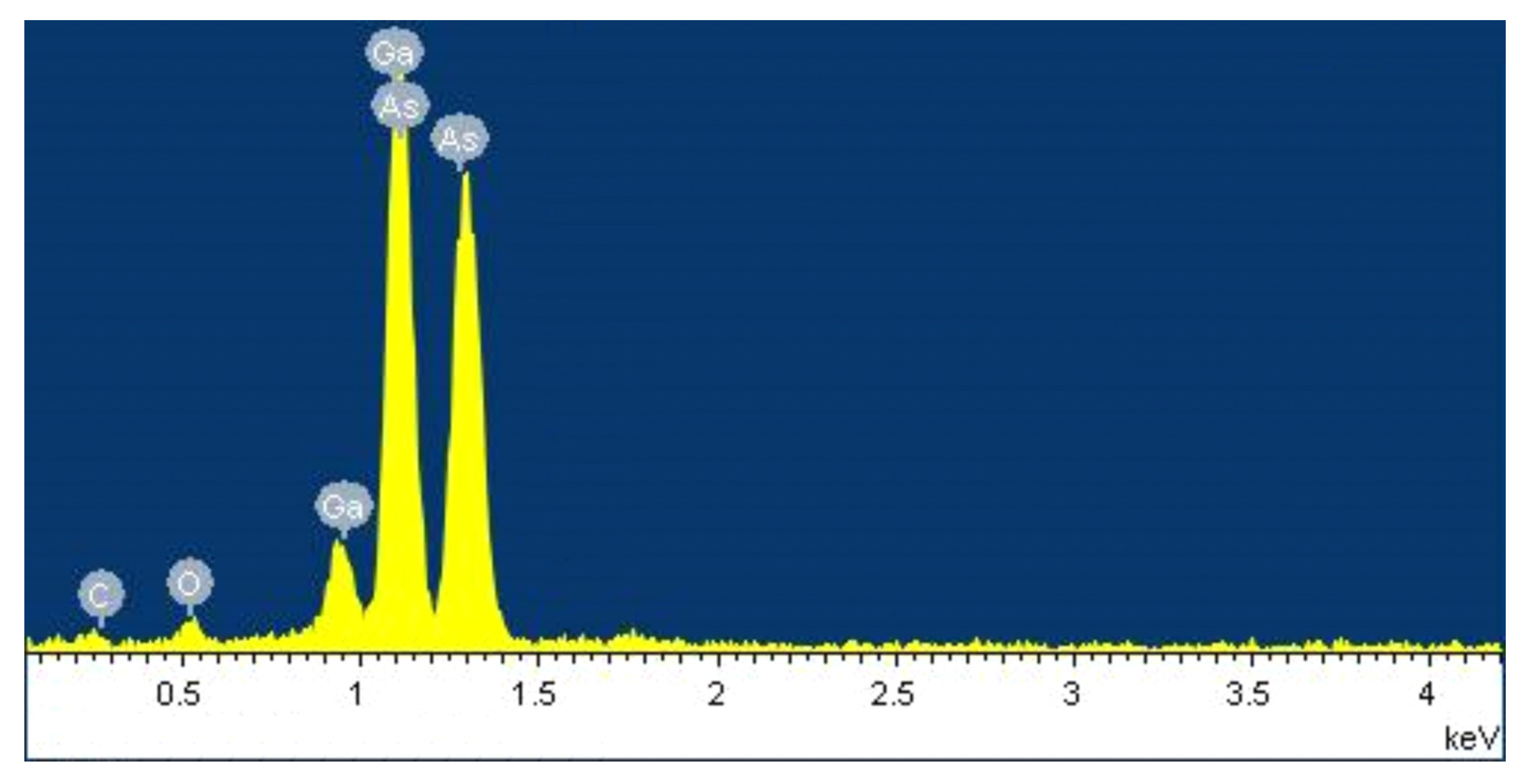
3. Results and Discussion

At the preliminary stage of the growth, the holes in the SiOx layer were unambiguously formed by In droplets etching. According to [26,27,28,29], a part of the deposited In adatoms on SiOx/Si substrate is oxidized because of oxygen migration from the SiOx overlayer. At this point, In oxides contribute to droplet self-organization by tuning In diffusion on the surface. During the following thermal annealing In oxidation plays the key role as it locally consumes the SiOx overlayer and drills nanoholes into SiOx until reaching the Si substrate. AFM profiles of the substrates surfaces (1 × 1 µm2) before and after etching, crystallization and evaporation of InAs from the surface are shown in Figure 1a,b. It is obvious that there are no holes in native-SiOx which are clearly resolved after In pre-treatment. It is important to note that the holes formed are uniform in depth ~0.6 nm. Based on the measurement results, the average surface density of the holes amounts to 1.9 × 1010 cm−2. Figure 1c shows the distribution of holes in lateral size. The difference in the sizes of the holes can be related to the different sizes of In droplets formed on the substrate surface and their evolution during annealing. To conclude this stage, the described substrate preparation method allows one to form holes in native-SiOx layers on Si(111) substrates.
Figure 2 shows typical SEM images of GaAs NWs grown on a native-SiOx/Si (111) substrate under the same growth conditions with and without In pre-treatment. As can be seen from the images, GaAs NWs without In pre-treatment follow different crystallographic directions and are inhomogeneous in morphological parameters. In turn, after In pre-treatment the NWs formed predominantly in the <111> direction. This means that NWs synthesis occurs epitaxially in the holes in SiOx/Si(111) surface. The average length of NWs is 3.5 μm, whereas the average surface density of NWs is about 2 × 10⁻⁶ cm−2. The difference in the densities of holes in SiOx and grown NWs may indicate that the NWs growth was initiated not in all of the holes. Indeed, most of the NWs have a diameter bigger than 50 nm, which is typical for Ga-catalyzed NWs growth [13]. According to the AFM measurements, only a small fraction of the holes exhibits lateral sizes bigger than 50 nm, that is why the NWs surface density is much smaller than the surface density of the holes. It should be noted that the diameter of the NWs bottom is not absolutely homogeneous. As the length increases to 500 nm, the NWs diameter decreases from 85 nm to 55 nm and then remains constant up to the top of the NWs. It turned out that, similar to the MBE growth using etching by Ga droplets [19], other rather flat objects were formed on the substrate surface, in addition to GaAs NWs.
For studying structural properties of the NWs, they were transferred from the substrate onto the carbon mesh. As shown in Figure 3, the structure of the NWs is predominantly cubic, which is typical for self-catalyzed GaAs NWs growth [13].
EDX analysis was carried out on several NWs. Figure 4 shows a typical EDX spectrum of GaAs NW. According to [30], peaks corresponding to In are observed in the EDX spectrum in the range from 3 to 4 keV. As can be seen from the figure, peaks corresponding to In are not observed in the EDX spectrum of grown NWs. Thus, indium was not detected along the entire length of NWs, which indicates its complete evaporation from the substrate surface before the GaAs NWs growth.
To conclude, we have shown the way to significantly decrease substrate temperature by introducing a procedure to create nanoscale holes in a native-SiOx layer on a Si(111) substrate via In-induced drilling. Using the fabricated template, we have successfully grown self-catalyzed GaAs nanowires by molecular-beam epitaxy. The fact that NWs formed in the <111> direction indicates that In droplets perfectly etch SiOx down to the silicon surface, and hence the NWs growth occurs epitaxially directly in the holes. Energy-dispersive X-ray analysis reveals no indium atoms inside the NWs. This unambiguously manifests that the procedure proposed can be used for the growth of ultra-pure GaAs NWs.

Author Contributions

Conceptualization, R.R.R. and G.E.C.; methodology, R.R.R. and A.I.K.; software, K.P.K.; validation, D.S.S., G.E.C., and E.V.U.; formal analysis, V.V.F.; investigation, E.V.U.; resources, A.I.K.; data curation, G.E.C.; writing-original draft preparation, R.R.R.; writing-review and editing, R.R.R.; visualization, K.P.K. and V.O.G.; supervision, G.E.C.; project administration, D.S.S.; funding acquisition, G.E.C. All authors have read and agreed to the published version of the manuscript.

Funding

The samples were grown under support of Ministry of Science and Higher Education of the Russian Federation (state task № 0791-2020-0003). AFM and SEM studies of the synthesized samples were supported by RFBR (grant 18-02-40006 mega). TEM studies were conducted using the facilities of Interdisciplinary Resource Center for Nanotechnology at Saint-Petersburg State University.

Conflicts of Interest

The authors declare no conflict of interest.

References

  1. Wong-Leung, J.; Yang, I.; Li, Z.; Karuturi, S.K.; Fu, L.; Tan, H.H.; Jagadish, C. Engineering III–V Semiconductor Nanowires for Device Applications. Adv. Mater. 2019, 32, e1904359. [Google Scholar] [CrossRef] [PubMed]
  2. Gudiksen, M.S.; Lauhon, L.J.; Wang, J.; Smith, D.C.; Lieber, C.M. Growth of nanowire superlattice structures for nanoscale photonics and electronics. Nature 2002, 415, 617–620. [Google Scholar] [CrossRef]
  3. Patolsky, F.; Zheng, G.; Hayden, O.; Lakadamyali, M.; Zhuang, X.; Lieber, C.M. Electrical detection of single viruses. Proc. Natl. Acad. Sci. USA 2004, 101, 14017–14022. [Google Scholar] [CrossRef] [Green Version]
  4. Сибирев, Н.; Kotlyar, K.; Koryakin, A.A.; Shtrom, I.V.; Ubiivovk, E.V.; Soshnikov, I.P.; Reznik, R.R.; Bouravleuv, A.D.; Cirlin, G. Solar Cell Based on Core/Shell Nanowires. Semiconductors 2018, 52, 1568–1572. [Google Scholar] [CrossRef]
  5. Glas, F. Critical dimensions for the plastic relaxation of strained axial heterostructures in free-standing nanowires. Phys. Rev. B 2006, 74, 121302. [Google Scholar] [CrossRef]
  6. Chuang, L.C.; Moewe, M.; Chase, C.; Kobayashi, N.P.; Chang-Hasnain, C.; Crankshaw, S. Critical diameter for III-V nanowires grown on lattice-mismatched substrates. Appl. Phys. Lett. 2007, 90, 43115. [Google Scholar] [CrossRef] [Green Version]
  7. Moewe, M.; Chuang, L.C.; Dubrovskii, V.G.; Chang-Hasnain, C. Growth mechanisms and crystallographic structure of InP nanowires on lattice-mismatched substrates. J. Appl. Phys. 2008, 104, 44313. [Google Scholar] [CrossRef] [Green Version]
  8. Wagner, R.S.; Ellis, W.C. Vapor-liquid-solid mechanism of single crystal growth. Appl. Phys. Lett. 1964, 4, 89. [Google Scholar] [CrossRef]
  9. Dubrovskii, V.G.; Cirlin, G.; Ustinov, V.M. Semiconductor nanowhiskers: Synthesis, properties, and applications. Semiconductors 2009, 43, 1539–1584. [Google Scholar] [CrossRef]
  10. Bullis, W. Properties of gold in silicon. Solid State Electron. 1966, 9, 143–168. [Google Scholar] [CrossRef]
  11. Perea, D.E.; Allen, J.E.; May, S.J.; Wessels, B.W.; Seidman, D.N.; Lauhon, L.J. Three-Dimensional Nanoscale Composition Mapping of Semiconductor Nanowires. Nano Lett. 2006, 6, 181–185. [Google Scholar] [CrossRef] [PubMed]
  12. Bar Sadan, M.; Barthel, J.; Shtrikman, H.; Houben, L. Direct Imaging of Single Au Atoms Within GaAs Nanowires. Nano Lett. 2012, 12, 2352–2356. [Google Scholar] [CrossRef] [Green Version]
  13. Cirlin, G.; Dubrovskii, V.G.; Samsonenko, Y.B.; Bouravleuv, A.D.; DuRose, K.; Proskuryakov, Y.Y.; Mendes, B.; Bowen, L.; Kaliteevski, M.A.; A Abram, R.; et al. Self-catalyzed, pure zincblende GaAs nanowires grown on Si(111) by molecular beam epitaxy. Phys. Rev. B 2010, 82, 035302. [Google Scholar] [CrossRef] [Green Version]
  14. Colombo, C.; Spirkoska, D.; Frimmer, M.; Abstreiter, G.; I Morral, A.F. Ga-assisted catalyst-free growth mechanism of GaAs nanowires by molecular beam epitaxy. Phys. Rev. B 2008, 77, 155326. [Google Scholar] [CrossRef]
  15. Jabeen, F.; Grillo, V.; Rubini, S.; Martelli, F. Self-catalyzed growth of GaAs nanowires on cleaved Si by molecular beam epitaxy. Nanotechnology 2008, 19, 275711. [Google Scholar] [CrossRef] [PubMed]
  16. Plissard, S.R.; Dick, K.A.; Larrieu, G.; Godey, S.; Addad, A.; Wallart, X.; Caroff, P. Gold-free growth of GaAs nanowires on silicon: Arrays and polytypism. Nanotechnology 2010, 21, 385602. [Google Scholar] [CrossRef] [PubMed]
  17. Reznik, R.R.; Kotlyar, K.P.; I Khrebtov, A.; Samsonenko, Y.B.; Soshnikov, I.P.; Dyakonov, V.; Zadiranov, U.M.; Tankelevskaya, E.M.; A Kudryashov, D.; Shevchuk, D.S.; et al. Development of methods for orderly growth of nanowires. J. Phys. Conf. Ser. 2015, 661, 012053. [Google Scholar] [CrossRef] [Green Version]
  18. I Morral, A.F.; Colombo, C.; Abstreiter, G.; Arbiol, J.; Morante, J.R. Nucleation mechanism of gallium-assisted molecular beam epitaxy growth of gallium arsenide nanowires. Appl. Phys. Lett. 2008, 92, 063112. [Google Scholar] [CrossRef] [Green Version]
  19. Küpers, H.; Bastiman, F.; Luna, E.; Somaschini, C.; Geelhaar, L. Ga predeposition for the Ga-assisted growth of GaAs nanowire ensembles with low number density and homogeneous length. J. Cryst. Growth 2017, 459, 43–49. [Google Scholar] [CrossRef]
  20. Tauchnitz, T.; Nurmamytov, T.; Hübner, R.; Engler, M.; Facsko, S.; Schneider, H.; Helm, M.; Dimakis, E. Decoupling the Two Roles of Ga Droplets in the Self-Catalyzed Growth of GaAs Nanowires on SiOx/Si(111) Substrates. Cryst. Growth Des. 2017, 17, 5276–5282. [Google Scholar] [CrossRef]
  21. Koivusalo, E.; Hakkarainen, T.V.; Guina, M.D.; Dubrovskii, V.G. Sub-Poissonian Narrowing of Length Distributions Realized in Ga-Catalyzed GaAs Nanowires. Nano Lett. 2017, 17, 5350–5355. [Google Scholar] [CrossRef] [PubMed]
  22. Schmidt, V.; Wittemann, J.V.; Senz, S.; Gösele, U. Silicon Nanowires: A Review on Aspects of their Growth and their Electrical Properties. Adv. Mater. 2009, 21, 2681–2702. [Google Scholar] [CrossRef]
  23. Egorov, A.; Kovsh, A.; Ustinov, V.; Zhukov, A.; Maksimov, M.; Cirlin, G.; Ledentsov, N.; Bimberg, D.; Werner, P.; Alferov, Z. Self-organized InAs quantum dots in a silicon matrix. J. Cryst. Growth 1999, 201, 1202–1204. [Google Scholar] [CrossRef]
  24. Zakharov, N.; Werner, P.; Gösele, U.; Heitz, R.; Bimberg, D.; Ledentsov, N.N.; Ustinov, V.M.; Volovik, B.V.; Alferov, Z.I.; Polyakov, N.K.; et al. Structure and optical properties of Si/InAs/Si layers grown by molecular beam epitaxy on Si substrate. Appl. Phys. Lett. 2000, 76, 2677–2679. [Google Scholar] [CrossRef]
  25. Cirlin, G.E.; Polyakov, N.K.; Petrov, V.N.; Egorov, V.A.; Samsonenko, Y.B.; Denisov, D.V.; Busov, V.M.; Volovik, B.V.; Ustinov, V.M.; Alferov, Z.I.; et al. Effect of growth conditions on InAs nanoislands formation on Si(100) surface. Czechoslov. J. Phys. 1999, 49, 1547–1552. [Google Scholar] [CrossRef]
  26. Fouquat, L.; Vettori, M.; Botella, C.; Benamrouche, A.; Penuelas, J.; Grenet, G. Early Stages of GaAs Nanowires VLS Self-Catalyzed Growth on Silica-terminated Silicon Substrate: A Photoemission Study; Cornell University: Ithaca, NY, USA, 2019. [Google Scholar]
  27. Sutter, E.; Sutter, P. Enhanced oxidation of nanoscale In particles at the interface with a Si nanowire. Appl. Phys. Lett. 2012, 100, 231602. [Google Scholar] [CrossRef]
  28. Ow-Yang, C.W.; Shigesato, Y.; Paine, D.C. Interfacial stability of an indium tin oxide thin film deposited on Si and Si0.85Ge0.15. J. Appl. Phys. 2000, 88, 3717–3724. [Google Scholar] [CrossRef]
  29. Kolluri, S.; Chandorkar, A. Effect of annealing on the surface and interface properties of indium oxide-silicon structures. Thin Solid Films 1993, 230, 39–44. [Google Scholar] [CrossRef]
  30. Koryakin, A.A.; Kukushkin, S.A.; Kotlyar, K.P.; Ubyivovk, E.; Reznik, R.R.; Cirlin, G. A new insight into the mechanism of low-temperature Au-assisted growth of InAs nanowires. CrystEngComm 2019, 21, 4707–4717. [Google Scholar] [CrossRef]
Figure 1. Typical AFM images of SiOx/Si(111) substrate surface: (a) initial and (b) after In droplets formation, etching, crystallization and evaporation of In from the surface. The scale bar corresponds to 250 nm. The insertion shows AFM image of a single hole in SiOx, which is approximately 35 nm in diameter (scale bar in the insertion corresponds to 50 nm); (c) Size distribution of holes in the SiOx layer diagram.
Materials 13 03449 g001
Figure 2. Typical SEM images of GaAs NWs grown on SiOx/Si(111) substrate: (a) without In pre-treatment; (b) with In pre-treatment.
Materials 13 03449 g002
Figure 3. (a) HAADF-STEM image of a single GaAs NW; (b) HR TEM image of a single GaAs NW.
Materials 13 03449 g003
Figure 4. Typical EDX spectrum of GaAs NW measured at the center of the NW.
Materials 13 03449 g004

