High-Quality Perovskite CH3NH3PbI3 Thin Films for Solar Cells Prepared by Single-Source Thermal Evaporation Combined with Solvent Treatment

 and
and 
Abstract
:1. Introduction
2. Experimental Details
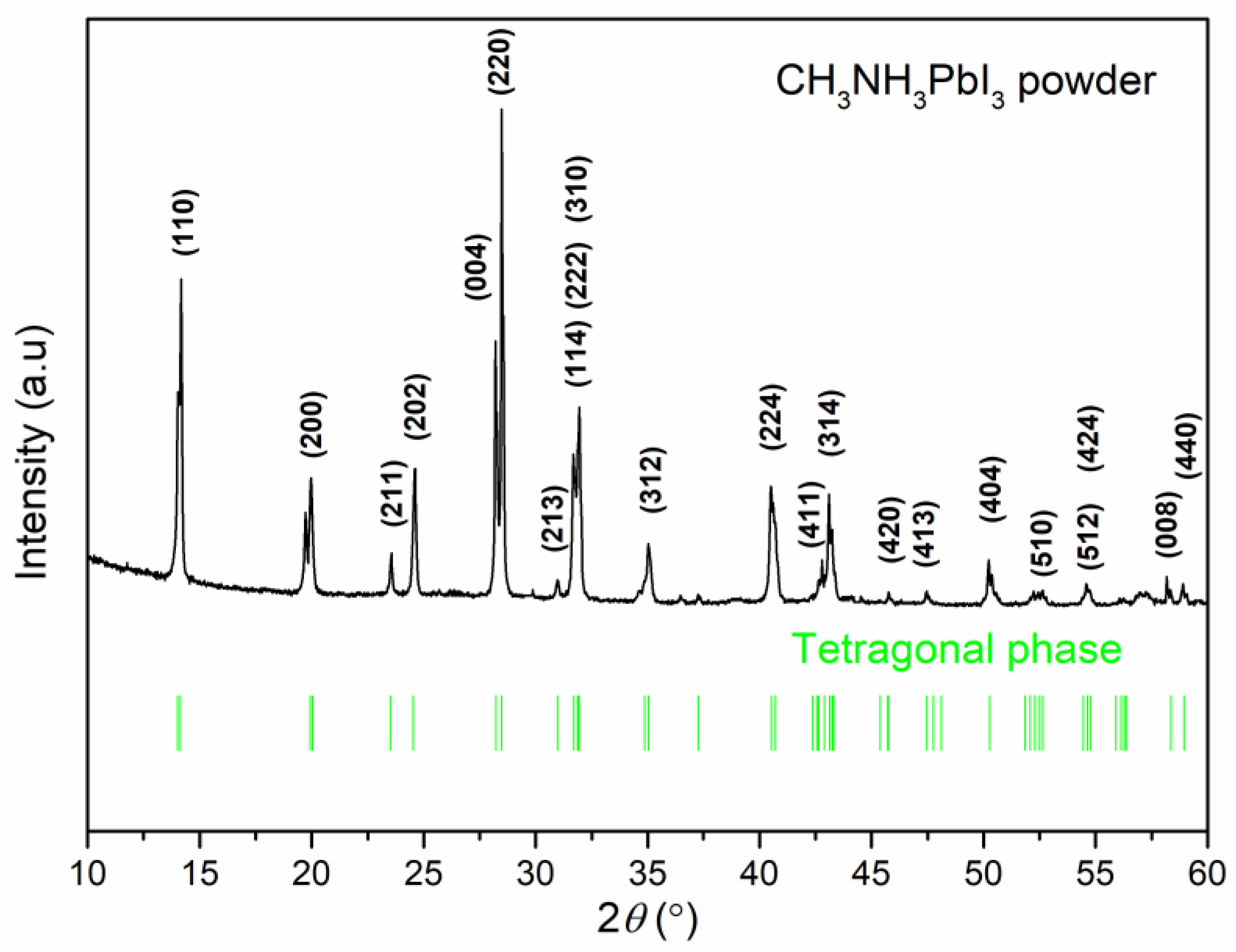
2.1. CH3NH3I and CH3NH3PbI3 Powder Preparation
2.2. Film Preparation
2.3. Device Fabrication
2.4. Characterization
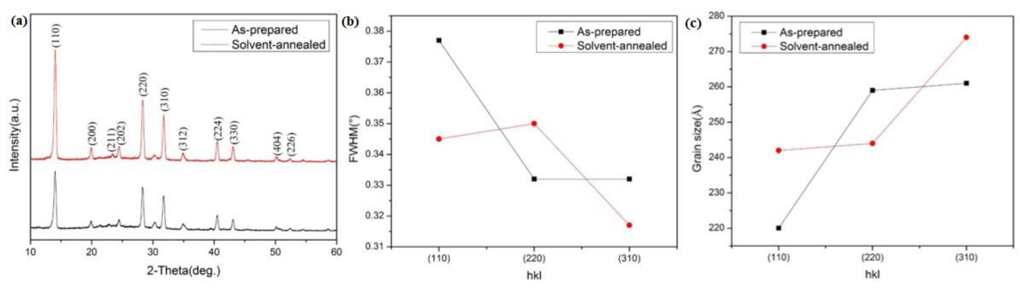
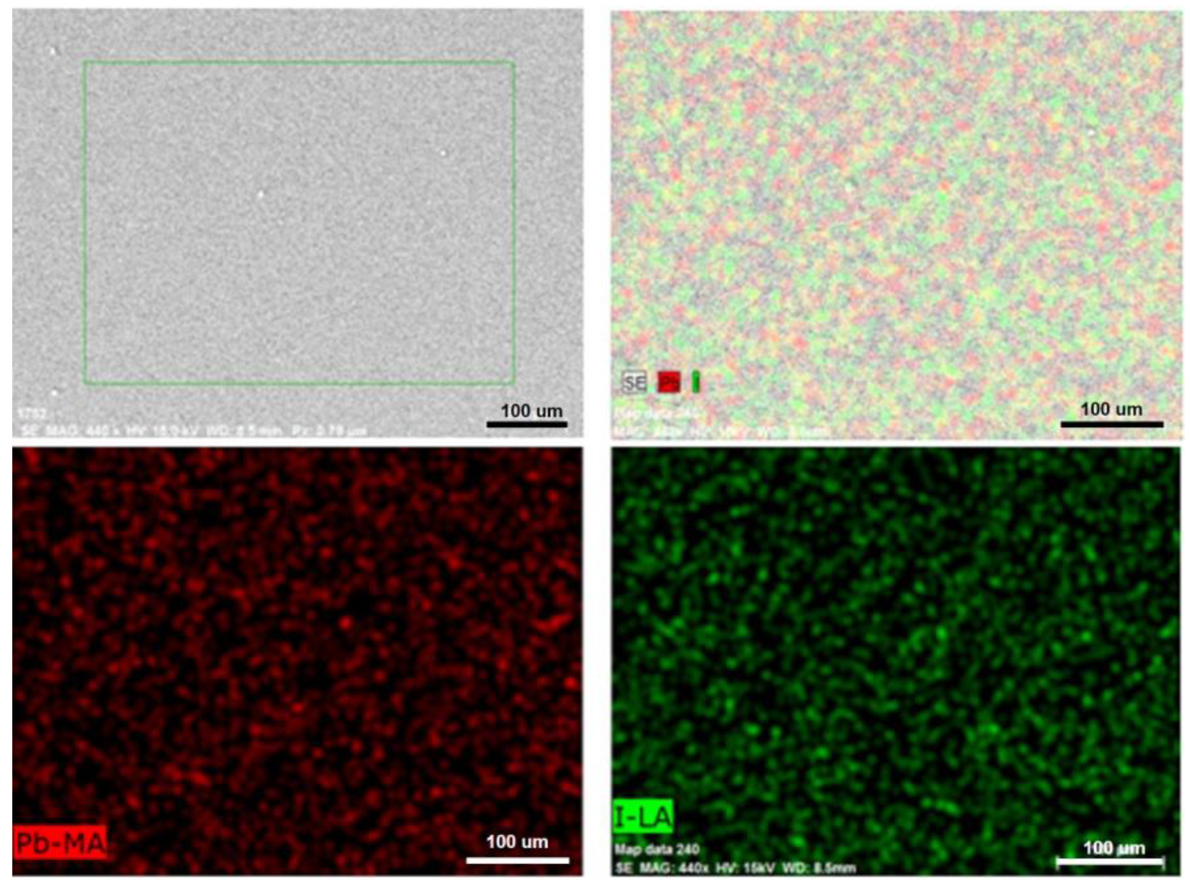
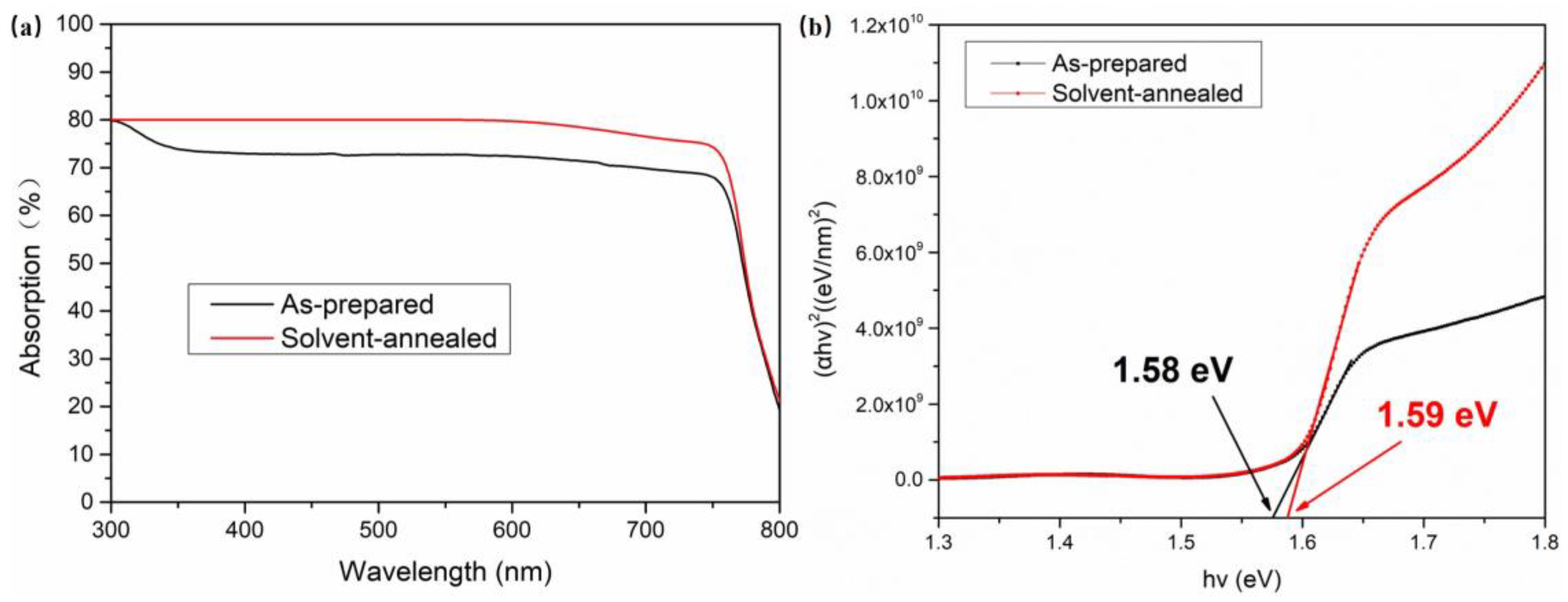
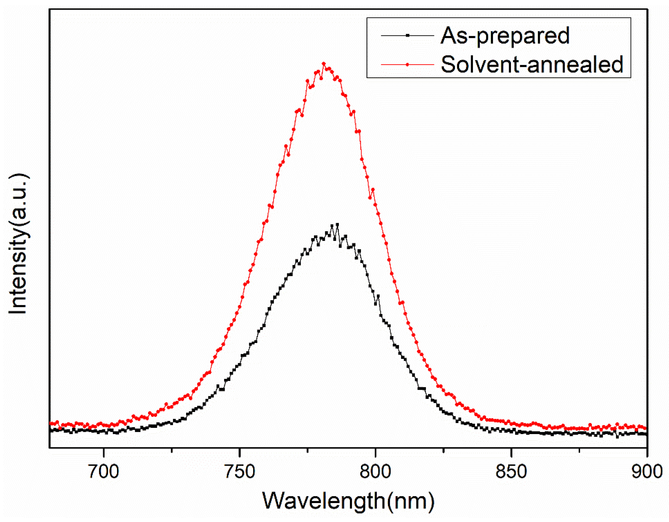
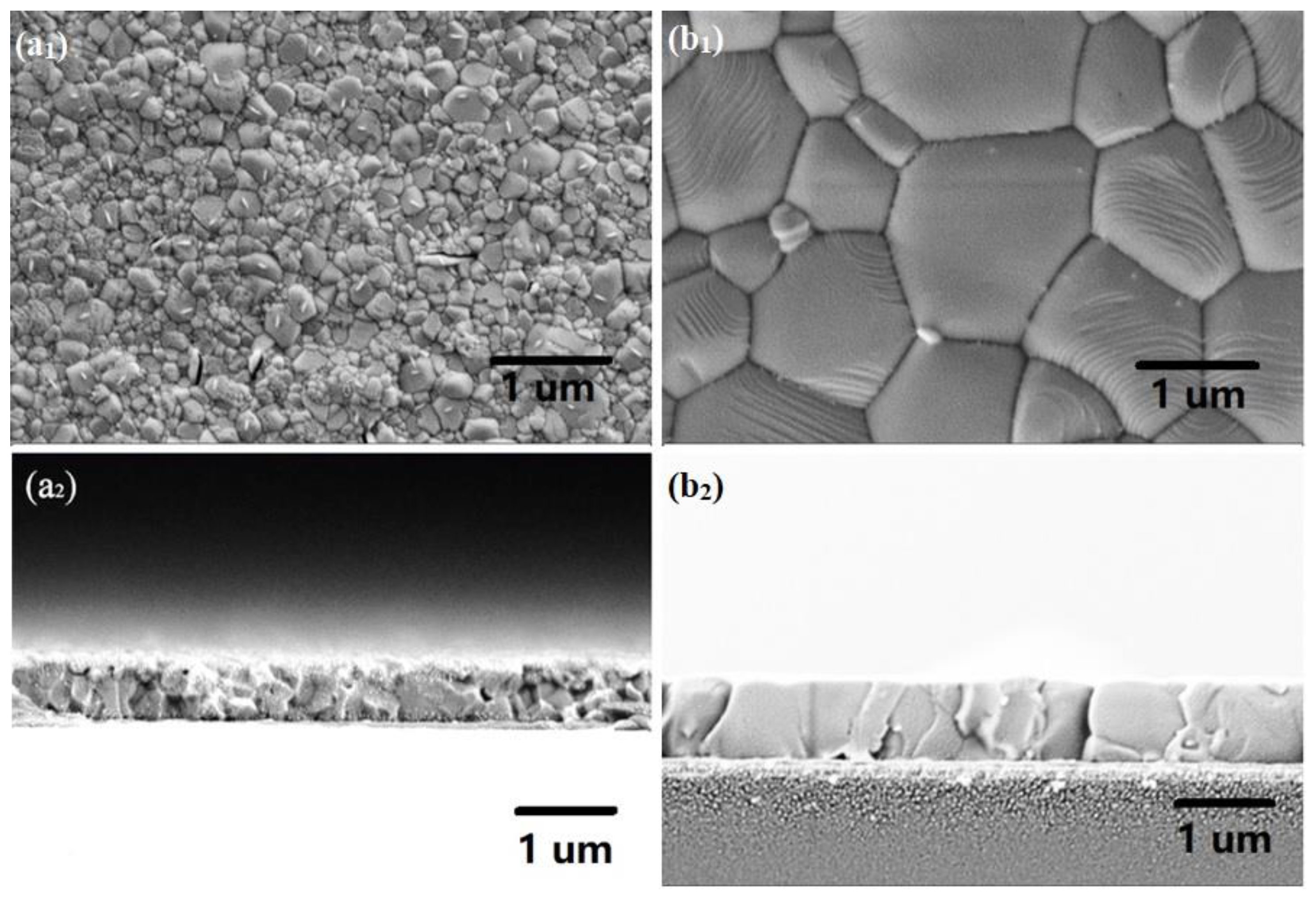
3. Results and Discussions
4. Conclusions
Author Contributions
Funding
Conflicts of Interest
References
- Seo, J.; Park, S.; Kim, Y.C.; Jeon, N.J.; Noh, J.H.; Yoon, S.C.; Seok, S.I. Benefits of very thin PCBM and LiF layers for solution-processed p-i-n perovskite solar cells. Energy Environ. Sci. 2014, 12, 2642–2646. [Google Scholar] [CrossRef]
- Saidaminov, M.I.; Abdelhady, A.L.; Murali, B.; Alarousu, E.; Burlakov, V.M.; Peng, W.; Dursun, I.; Wang, L.; He, Y.; Maculan, G.; et al. High-quality bulk hybrid perovskite single crystals within minutes by inverse temperature crystallization. Nat. Commun. 2015, 6, 7586. [Google Scholar] [CrossRef]
- Chiang, C.; Wu, C. Bulk heterojunction perovskite-PCBM solar cells with high fill factor. Nat. Photonics 2016, 3, 196–200. [Google Scholar] [CrossRef]
- Leblebici, S.Y.; Leppert, L.; Li, Y.; Reyes-Lillo, S.E.; Wickenburg, S.; Wong, E.; Lee, J.; Melli, M.; Ziegler, D.; Angell, D.K.; et al. Facet-dependent photovoltaic efficiency variations in single grains of hybrid halide perovskite. Nat. Energy 2016, 93, 16093. [Google Scholar] [CrossRef]
- Leijtens, T.; Lauber, A.; Eperson, G.E.; Stranks, S.D.; Snaith, H.J. The importance of perovskite pore filling in organometal mixed halide sensitized TiO2-based solar cells. J. Phys. Chem. Lett. 2014, 5, 1096–1102. [Google Scholar] [CrossRef] [PubMed]
- Wang, Q.; Shao, Y.; Dong, Q.; Xiao, Z.; Yuan, Y.; Huang, J. Large fill-factor bilayer iodine perovskite solar cells fabricated by a low-temperature solution-processed. Energy Environ. Sci. 2014, 7, 2359–2365. [Google Scholar] [CrossRef]
- Nie, W.; Tsai, H.; Asadpour, R.; Blancon, J.C.; Neukirch, A.J.; Gupta, G.; Crochet, J.J.; Chhowalla, M.; Tretiak, S.; Alam, M.A.; et al. High-efficiency solution-processed perovskite solar cells with millimeter-scale grains. Science 2015, 347, 522–525. [Google Scholar] [CrossRef] [PubMed]
- Liang, P.W.; Liao, C.Y.; Chueh, C.C.; Zuo, F.; Williams, S.T.; Xin, X.K.; Lin, J.; Jen AK, Y. Additive enhanced crystallization of solution-processed perovskite for highly efficient planar-heterojunction solar cells. Adv. Mater. 2014, 26, 3748–3754. [Google Scholar] [CrossRef]
- Mosconi, E.; Amat, A.; Nazeeruddin, M.K.; Gratzel, M.; Angelis, F.D. First-principles modeling of mixed halide organomental perovskites for photovoltaic applications. J. Phys. Chem. C 2013, 117, 13902–13913. [Google Scholar] [CrossRef]
- Zhao, Y.X.; Zhu, K. CH3NH3Cl-assisted one-step solution growth of CH3NH3PbI3:structure, charge-carrier dynamics, and photovoltaic properties of perovskite solar cells. J. Phys. Chem. C 2014, 118, 9412–9418. [Google Scholar] [CrossRef]
- Heo, J.H.; Song, D.H.; Im, S.H. Planar CH3NH3PbBr3 hybrid solar cells with 10.4% power conversion efficiency, fabricated by controlled crystallization in the spin-coating process. Adv. Mater. 2014, 26, 8179–8183. [Google Scholar] [CrossRef]
- Liang, G.X.; Fan, P.; Luo, J.T.; Gu, D.; Zheng, Z.H. A promising unisource thermal evaporation for in situ fabrication of organolead halide perovskite CH3NH3PbI3 thin film. Prog. Photovolt. Res. Appl. 2015, 23, 1901–1907. [Google Scholar] [CrossRef]
- Fan, P.; Gu, D.; Liang, G.X.; Chen, J.L.; Luo, J.T.; Xie, Y.Z.; Zheng, Z.H.; Zhang, D.P. Growth of high quality CH3NH3PbI3 thin films prepared by modified dual-source vapor evaporation. J. Mater. Sci. Mater. Electron. 2016, 3, 2321–2327. [Google Scholar] [CrossRef]
- Fan, P.; Gu, D.; Liang, G.X.; Luo, J.T.; Chen, J.L.; Zheng, Z.H.; Zhang, D.P. High-performance perovskite CH3NH3PbI3 thin films for solar cells prepared by single-source physical vapour deposition. Sci. Rep. 2016, 6, 29910. [Google Scholar] [CrossRef]
- Chen, J.L.; Fan, P.; Liang, G.X.; Gu, D.; Luo, J.T.; Zheng, Z.H.; Zhao, J.; Zhang, D.P. Doped tin induced structural evaluation and performance of CH3NH3PbxSn1−xI3 thin films prepared by a single route of unisource thermal evaporation. J. Mater. Sci. Mater. Electron. 2016, 12, 13192–13198. [Google Scholar] [CrossRef]
- Xiao, M.; Huang, F.; Huang, W.; Dkhissi, Y.; Etheridge, J.; Gray-Weale, A.; Bach, U.; Cheng, Y.A.; Spiccia, L. A fast deposition-crystallization procedure for highly efficient lead iodide perovskite thin-film solar cells. Angew. Chem. Int. Ed. 2014, 53, 9898–9903. [Google Scholar] [CrossRef]
- Huang, F.; Dkhissi, Y.; Huang, W.; Xiao, M.; Benesperi, I.; Rubanov, S.; Zhu, Y.; Lin, X.; Jiang, L.; Zhou, Y.; et al. Gas-assisted preparation of lead iodide perovskite films consisting of a monolayer of single crystalline grains for high efficiency planar solar cells. Nano Energy 2014, 10, 10–18. [Google Scholar] [CrossRef]
- Jeon, N.J.; Noh, J.H.; Kim, Y.C.; Yang, W.S.; Ryu, S.; Seok, S.I. Solvent engineering for high-performance inorganic-organic hybrid perovskite solar cells. Nat. Mater. 2014, 13, 897. [Google Scholar] [CrossRef]
- Jung, J.W.; Williams, S.T.; Jen, A.K.Y. Low-temperature processed high-performance flexible perovskite solar cells via rationally optimized solvent washing treatments. RSC Adv. 2014, 4, 62971–62977. [Google Scholar] [CrossRef]
- Cui, J.; Meng, F.P.; Zhang, H.; Cao, K.; Yuan, H.L.; Cheng, Y.B.; Huang, F.; Wang, M.K. CH3NH3PbI3-based planar solar cells with magnetron-sputtered nickel oxide. ACS Appl. Mater. Interfaces 2014, 6, 22862–22870. [Google Scholar] [CrossRef]
- Xiao, Z.G.; Dong, Q.F.; Bi, C.; Shao, Y.C.; Yuan, Y.B.; Huang, J.S. Solvent Annealing of Perovskite-Induced Crystal Growth for Photovoltaic-Device Efficiency Enhancement. Mater. Views 2014, 26, 6503–6509. [Google Scholar] [CrossRef] [PubMed]
- Li, X.; Bi, D.Q.; Yi, C.Y.; Decoppet, D.J.; Luo, J.S.; Zakeeruddin, S.M.; Hagfeldt, A.; Gratzel, M. A vaccum flash-assisted solution process for high-efficiency large-area perovskite solar cells. Science 2016, 353, 58–62. [Google Scholar] [CrossRef] [PubMed]
- Heo, J.H.; Im, S.H. CH3NH3PbI3/poly-3-hexylthiophen perovskite mesoscopic solar cells: Performance enhancement by Li-assisted hole conduction. Phys. Status Solidi (RRL) Rapid Res. Lett. 2014, 8, 816–821. [Google Scholar] [CrossRef]
- Mitzi, D.B. Templating and structural engineering in organic-inorganic perovskites. J. Chem. Soc.-Dalton Trans. 2001, 1, 1–12. [Google Scholar] [CrossRef]
- Baikie, T.; Fang, Y.; Kadro, J.M.; Schreyer, M.; Wei, F.; Mhaisalkar, S.G.; Graetzel, M.; White, T.J. Synthesis and crystal chemistry of the hybrid perovskite (CH3NH3)PbI3 for solid-state sensitised solar cell applications. J. Mater. Chem. A 2013, 1, 5628–5641. [Google Scholar] [CrossRef]


| Sample | Pb (at.%) | I (at.%) | Pb/I |
|---|---|---|---|
| As-deposited films | 24.75 | 75.25 | 1/3.04 |
| Annealed films | 24.76 | 75.24 | 1/3.03 |
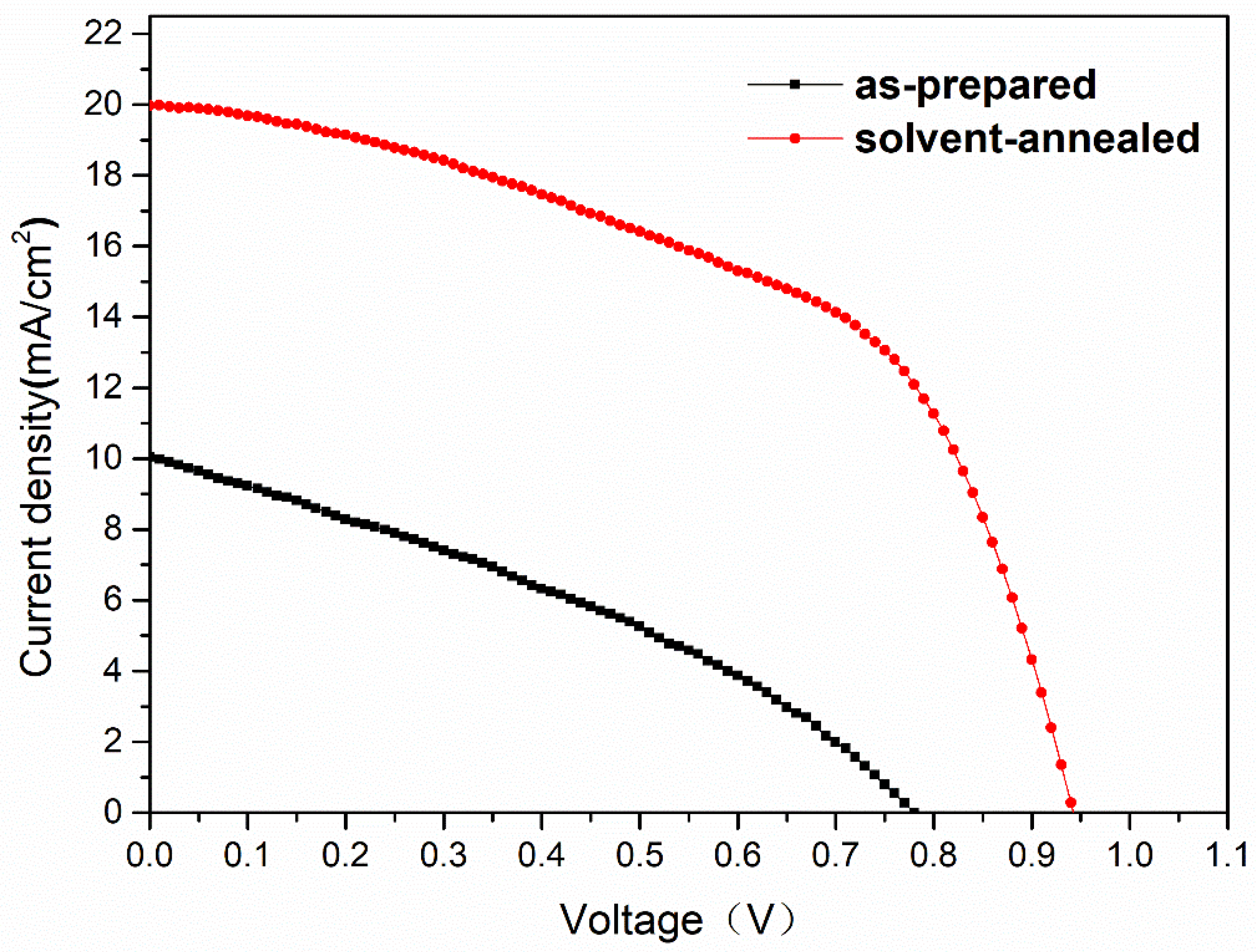
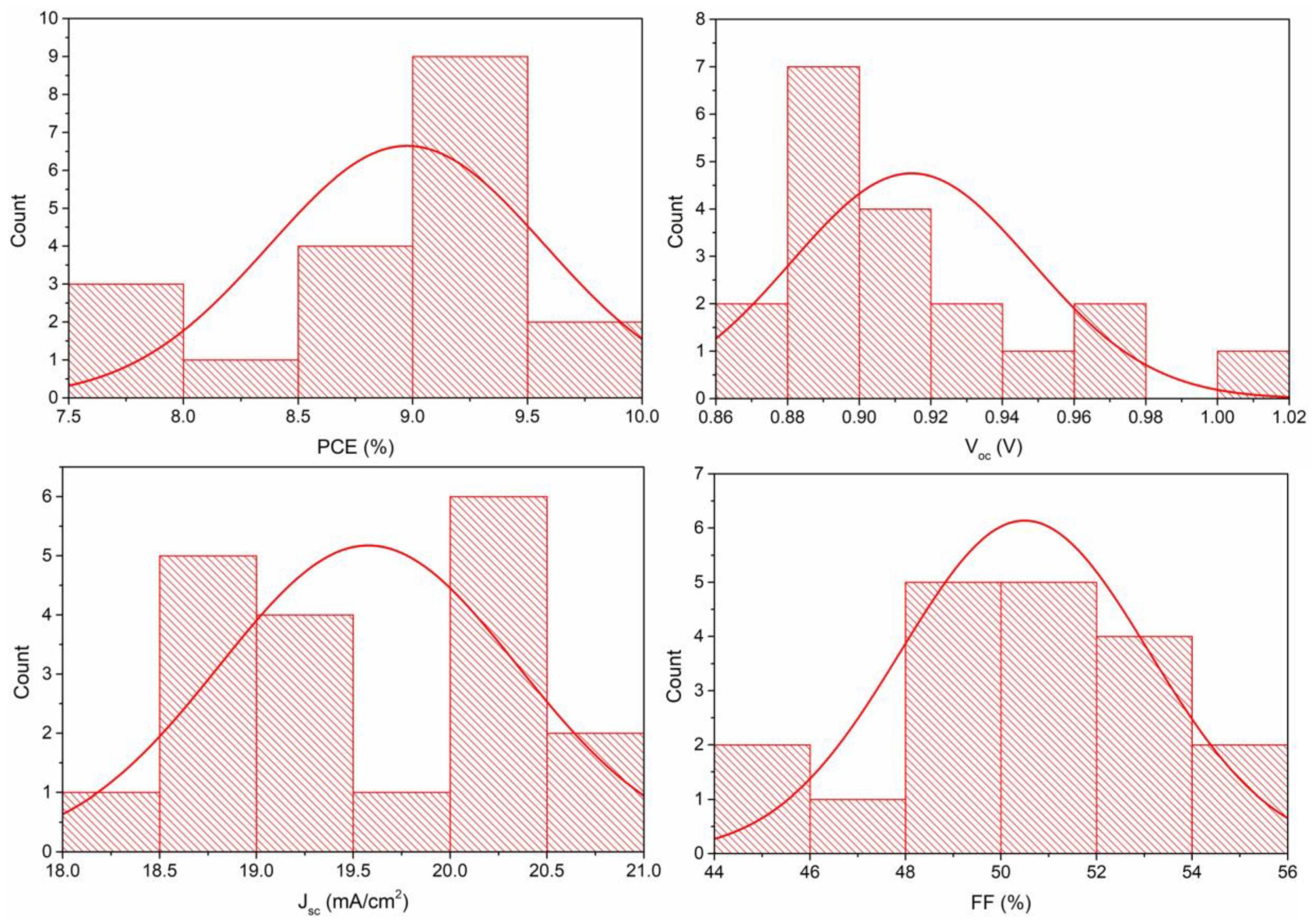
| Sample | Jsc (mA/cm2) | Voc (V) | FF (%) | PCE (%) |
|---|---|---|---|---|
| As-prepared | 10.04 | 0.77 | 34 | 2.64 |
| Solvent-annealed | 19.97 | 0.94 | 53 | 9.92 |
© 2019 by the authors. Licensee MDPI, Basel, Switzerland. This article is an open access article distributed under the terms and conditions of the Creative Commons Attribution (CC BY) license (http://creativecommons.org/licenses/by/4.0/).
Share and Cite
Peng, H.; Su, Z.; Zheng, Z.; Lan, H.; Luo, J.; Fan, P.; Liang, G. High-Quality Perovskite CH3NH3PbI3 Thin Films for Solar Cells Prepared by Single-Source Thermal Evaporation Combined with Solvent Treatment. Materials 2019, 12, 1237. https://doi.org/10.3390/ma12081237
Peng H, Su Z, Zheng Z, Lan H, Luo J, Fan P, Liang G. High-Quality Perovskite CH3NH3PbI3 Thin Films for Solar Cells Prepared by Single-Source Thermal Evaporation Combined with Solvent Treatment. Materials. 2019; 12(8):1237. https://doi.org/10.3390/ma12081237
Chicago/Turabian StylePeng, Huanxin, Zhenghua Su, Zhuanghao Zheng, Huabin Lan, Jingting Luo, Ping Fan, and Guangxing Liang. 2019. "High-Quality Perovskite CH3NH3PbI3 Thin Films for Solar Cells Prepared by Single-Source Thermal Evaporation Combined with Solvent Treatment" Materials 12, no. 8: 1237. https://doi.org/10.3390/ma12081237
APA StylePeng, H., Su, Z., Zheng, Z., Lan, H., Luo, J., Fan, P., & Liang, G. (2019). High-Quality Perovskite CH3NH3PbI3 Thin Films for Solar Cells Prepared by Single-Source Thermal Evaporation Combined with Solvent Treatment. Materials, 12(8), 1237. https://doi.org/10.3390/ma12081237