Understanding Current Instabilities in Conductive Atomic Force Microscopy

Abstract
:1. Introduction
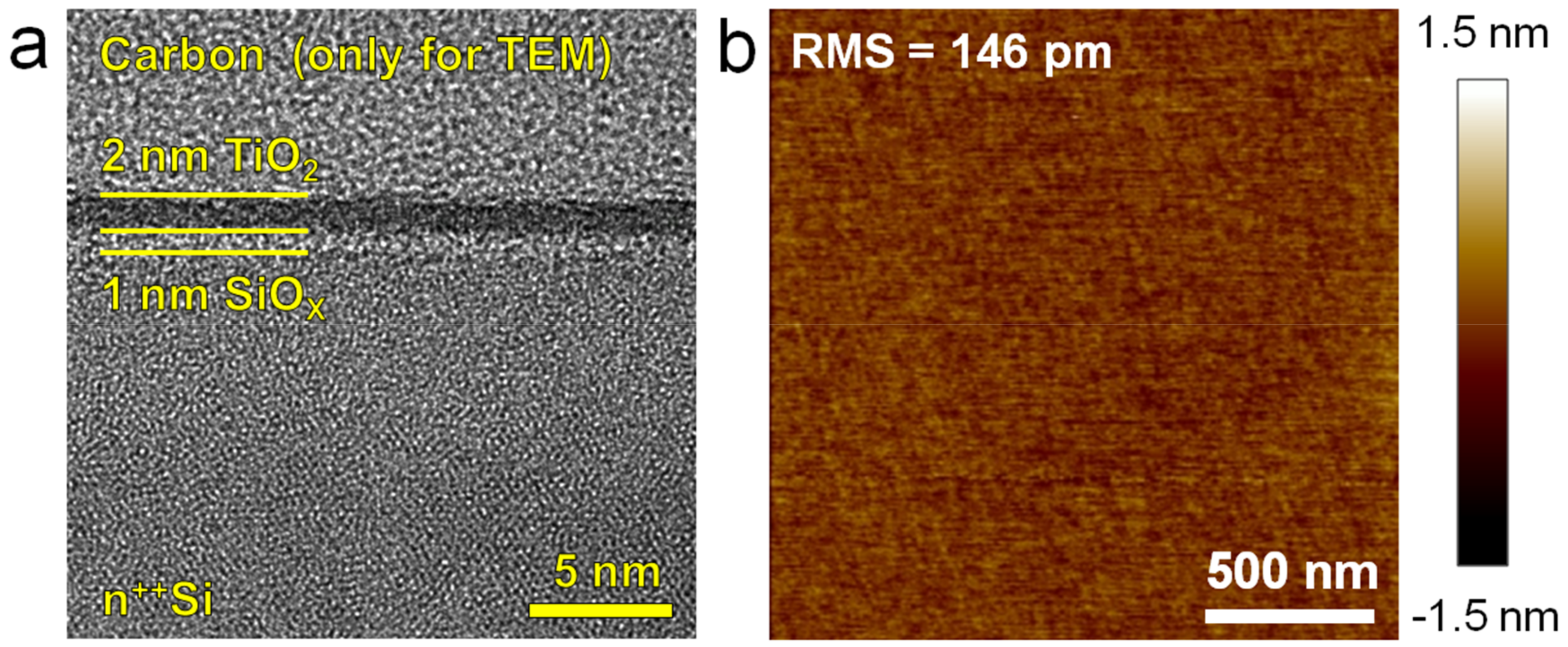
2. Experimental
3. Results and Discussion
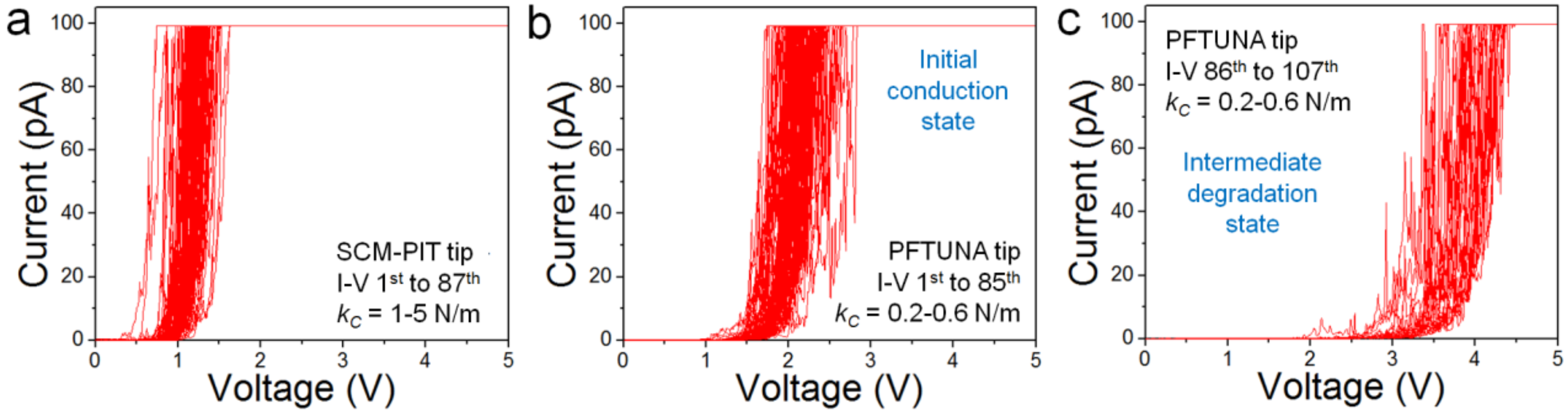
3.1. Degradation of the CAFM Tip
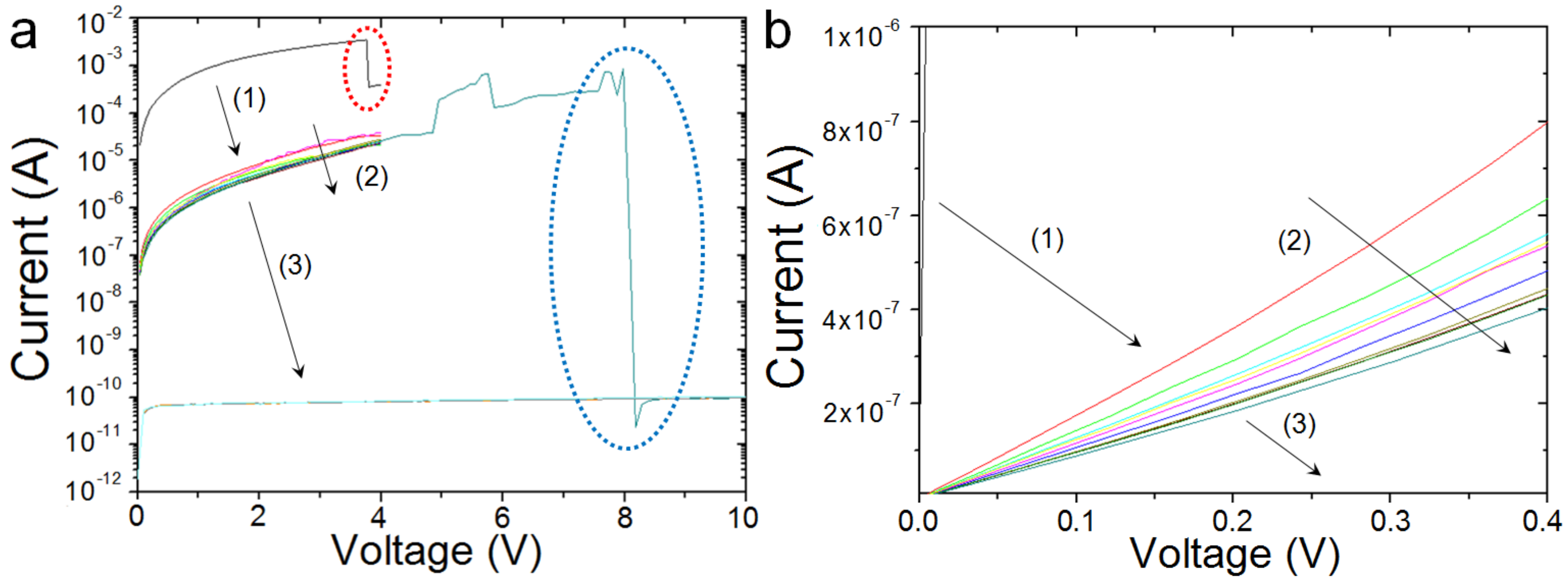
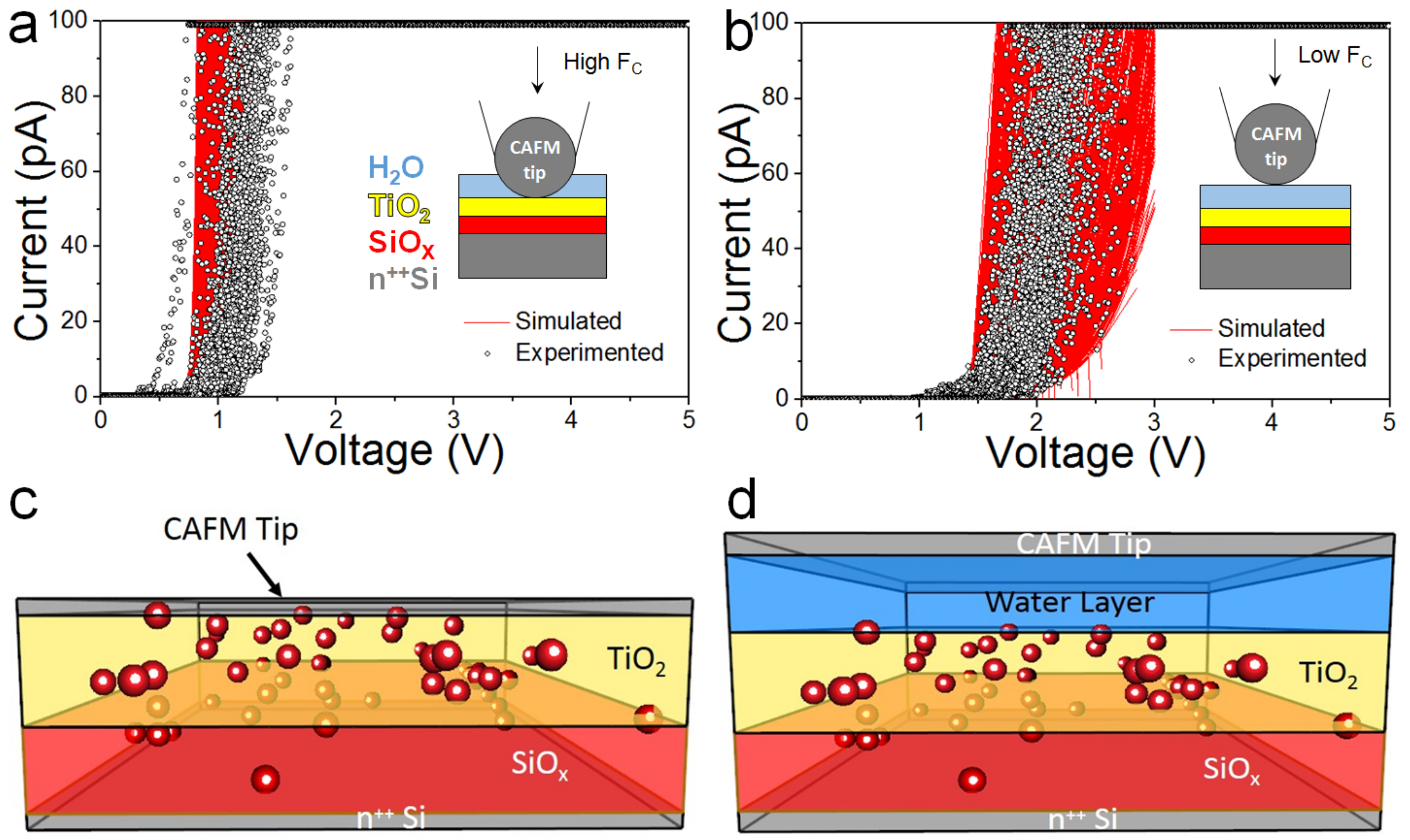
3.2. Presence of H2O at the Tip/Sample Junction
4. Conclusions
Author Contributions
Funding
Acknowledgments
Conflicts of Interest
References
- Murrell, M.P.; Welland, M.E.; O’Shea, S.J.; Wong, T.M.H.; Barnes, J.R.; McKinnon, A.W.; Heyns, M.; Verhaverbeke, S. Spatially resolved electrical measurements of SiO2 gate oxides using atomic force microscopy. Appl. Phys. Lett. 1993, 62, 786. [Google Scholar] [CrossRef]
- Pan, C.; Shi, Y.; Hui, F.; Gutierrez, E.G.; Lanza, M. History and Status of the CAFM. In Conductive Atomic Force Microscopy: Applications in Nanomaterials; Lanza, M., Ed.; Wiley-VCH: Suzhou, China, 2017; pp. 1–18. [Google Scholar]
- Wu, Q.; Bayerl, A.; Porti, M.; Martínez, J.M.; Lanza, M.; Rodriguez, R.; Velayudhan, V.; Nafria, M.; Aymerich, X.; Gonzalez, M.B.; et al. A Conductive AFM Nanoscale Analysis of NBTI and Channel Hot-Carrier Degradation in MOSFETs. IEEE Trans. Electron Devices 2014, 61, 3118–3124. [Google Scholar] [CrossRef]
- Krause, O. Fabrication and Reliability of Conductive AFM Probes. In Conductive Atomic Force Microscopy: Applications in Nanomaterials; Lanza, M., Ed.; Wiley-VCH: Suzhou, China, 2017; pp. 29–44. [Google Scholar]
- Rocky Mountain Nanotechnology: Technical Data. Available online: http://rmnano.com/tech.html (accessed on 20 April 2018).
- Imec: Solid Diamond AFM Probes Datasheet. Available online: https://www.brukerafmprobes.com/images/product/specPDF/3820.pdf (accessed on 21 April 2018).
- Hui, F.; Chen, S.; Liang, X.; Yuan, B.; Jing, X.; Shi, Y.; Lanza, M. Graphene Coated Nanoprobes: A Review. Crystals 2017, 7, 269. [Google Scholar] [CrossRef]
- Hui, F.; Vajha, P.; Shi, Y.; Ji, Y.; Duan, H.; Padovani, A.; Larcher, L.; Li, X.R.; Xu, J.J.; Lanza, M. Moving graphene devices from lab to market: Advanced graphene-coated nanoprobes. Nanoscale 2016, 8, 8466. [Google Scholar] [CrossRef] [PubMed]
- Hui, F.; Vajha, P.; Ji, Y.; Pan, C.; Gutierrez, E.G.; Duan, H.; He, P.; Ding, G.; Shi, Y.; Lanza, M. Variability of graphene devices fabricated using graphene inks: Atomic force microscope tips. Surf. Coat. Technol. 2017, 320, 391–395. [Google Scholar] [CrossRef]
- Weeks, B.L.; Vaughn, M.W. Direct imaging of meniscus formation in atomic force microscopy using environmental scanning electron microscopy. Langmuir 2005, 21, 8096–8098. [Google Scholar] [CrossRef] [PubMed]
- Kremmer, S.; Peissl, S.; Teichert, C.; Kuchar, F.; Hofer, H. Modification and characterization of thin silicon gate oxides using conducting atomic force microscopy. Mater. Sci. Eng. B 2003, 102, 88–93. [Google Scholar] [CrossRef]
- Parksystems.com: Park NX-Hivac. Available online: www.parksystems.com/index.php/products/small-sample-afm/park-nx-hivac (accessed on 20 April 2018).
- Hitachi-hightech.com: Hitachi AFM5300E. Available online: https://www.hitachi-hightech.com/global/science/products/microscopes/afm/units/afm5300e.html (accessed on 20 April 2018).
- Scientaomicron.com: Fermi DryCool SPM. Available online: http://www.scientaomicron.com/en/products/434/1386 (accessed on 20 April 2018).
- Xiao, N.; Villena, M.A.; Yuan, B.; Chen, S.; Wang, B.; Eliáš, M.; Shi, Y.; Hui, F.; Jing, X.; Scheuerman, A.; et al. Resistive random access memory cells with a bilayer TiO2/SiOx insulating stack for simultaneous filamentary and distributed resistive switching. Adv. Funct. Mater. 2017, 1700384. [Google Scholar] [CrossRef]
- Frammelsberger, W.; Benstetter, G.; Kiely, J.; Stamp, R. C-AFM-based thickness determination of thin and ultra-thin SiO2 films by use of different conductive-coated probe tips. Appl. Surf. Sci. 2007, 253, 3615–3626. [Google Scholar] [CrossRef]
- Lanza, M.; Porti, M.; Nafría, M.; Aymerich, X.; Benstetter, G.; Lodermeier, E.; Ranzinger, H.; Jaschke, G.; Teichert, S.; Wilde, L.; et al. Conductivity and charge trapping after electrical stress in amorphous and polycristalline Al2O3 based devices studied with AFM related techniques. IEEE Trans. Nanotechnol. 2011, 10, 344–351. [Google Scholar] [CrossRef]
- Lanza, M.; Porti, M.; Nafría, M.; Aymerich, X.; Benstetter, G.; Lodermeier, E.; Ranzinger, H.; Jaschke, G.; Teichert, S.; Wilde, L.; et al. Crystallization and silicon diffusion nanoscale effects on the electrical properties of Al2O3 based devices. Microelectron. Eng. 2009, 86, 1921–1924. [Google Scholar] [CrossRef]
- Shi, Y.; Ji, Y.; Sun, H.; Hui, F.; Hu, J.; Wu, Y.; Fang, J.; Lin, H.; Wang, J.; Duan, H.; et al. Nanoscale characterization of PM2.5 airborne pollutants reveals high adhesiveness and aggregation capability of soot particles. Nat. Sci. Rep. 2015, 5, 11232. [Google Scholar] [CrossRef] [PubMed]
- Ji, Y.; Hui, F.; Shi, Y.; Han, T.; Song, X.; Pan, C.; Lanza, M. Fabrication of a fast-response and user-friendly environmental chamber for atomic force microscopes. Rev. Sci. Instrum. 2015, 86, 106105. [Google Scholar] [CrossRef] [PubMed]
- Lee, G.; Yu, Y.; Lee, C.; Dean, C.; Shepard, K.L.; Kim, P.; Hone, J. Electron tunneling through atomically flat and ultrathin hexagonal boron nitride. Appl. Phys. Lett. 2011, 99, 243114. [Google Scholar] [CrossRef]
- Houzé, F.; Meyer, R.; Schneegans, O.; Boyer, L. Imaging the local electrical properties of metal surfaces by atomic force microscopy with conducting probes. Appl. Phys. Lett. 1996, 69, 1975. [Google Scholar] [CrossRef]
- Infante, I.C.; Sánchez, F.; Laukhin, V.; del Pino, A.P.; Fontcuberta, J.; Bouzehouane, K.; Fusil, S.; Barthélémy, A. Functional characterization of SrTiO3 tunnel barriers by conducting atomic force microscopy. Appl. Phys. Lett. 2006, 89, 172506. [Google Scholar] [CrossRef]
- Félix, L.A.; Sirena, M.; Guzmán, L.A.A.; Sutter, J.G.; Vargas, S.P.; Steren, L.B.; Bernard, R.; Trastoy, J.; Villegas, J.E.; Briático, J.; et al. Structural and electrical characterization of ultra-thin SrTiO3 tunnel barriers grown over YBa2Cu3O7 electrodes for the development of high Tc Josephson junctions. Nanotechnology 2012, 23, 495715. [Google Scholar] [CrossRef] [PubMed]
- Lanza, M.; Bayerl, A.; Gao, T.; Porti, M.; Nafria, M.; Jing, G.; Zhang, Y.; Liu, Z.; Duan, H. Graphene-coated Atomic Force Microscope tips for reliable nanoscale electrical characterization. Adv. Mater. 2013, 25, 1440–1444. [Google Scholar] [CrossRef]
- Shi, Y.; Ji, Y.; Hui, F.; Iglesias, V.; Marc Porti, M.; Nafria, M.; Miranda, E.; Bersuker, G.; Lanza, M. Elucidating the origin of resistive switching in ultrathin hafnium oxides through high spatial resolution tools. ECS Trans. 2014, 64, 19–28. [Google Scholar] [CrossRef]
- Aguilera, L.; Lanza, M.; Bayerl, A.; Porti, M.; Nafria, M.; Aymerich, X. Development of a conductive atomic force microscope with a logarithmic current-to-voltage converter for the study of metal oxide semiconductor gate dielectrics reliability. J. Vac. Sci. Technol. B 2009, 27, 360–363. [Google Scholar] [CrossRef]
- Palumbo, F.; Liang, X.; Yuan, B.; Shi, Y.; Hui, F.; Villena, M.A.; Lanza, M. Bimodal dielectric breakdown in electronic devices using chemical vapor deposited hexagonal boron nitride as dielectric. Adv. Electron. Mater. 2018, 1700506. [Google Scholar] [CrossRef]
- Xu, J.; Xu, J.; Zhang, P.; Li, W.; Chen, K. Nanoscale quantification of charge injection and transportation process in Si-nanocrystal based sandwiched structure. Nanoscale 2013, 5, 9971. [Google Scholar] [CrossRef] [PubMed]
- Bolsée, J.; Oosterbaan, W.D.; Lutsen, L.; Vanderzande, D.; Manca, J. CAFM on conjugated polymer nanofibers: Capable of assessing one fiber mobility. Org. Electron. 2011, 12, 2084–2089. [Google Scholar] [CrossRef]
- Lanza, M.; Porti, M.; Nafria, M.; Benstetter, G.; Frammelsberger, W.; Ranzinger, H.; Lodermeier, E.; Jaschke, G. Influence of the manufacturing process on the electrical properties of thin (<4 nm) Hafnium based high-k stacks observed with CAFM. Microelectron. Reliab. 2007, 47, 1424–1428. [Google Scholar] [CrossRef]
- Lanza, M.; Iglesias, V.; Porti, M.; Nafría, M.; Aymerich, X. Polycrystallization effects on the variability of the electrical properties of high-k dielectrics at the nanoscale. Nanoscale Res. Lett. 2011, 6, 108. [Google Scholar] [CrossRef]
- Larcher, L.; Puglisi, F.M.; Padovani, A.; Vandelli, L.; Pavan, P. Multiscale modeling of electron-ion interactions for engineering novel electronic devices and materials. In Proceedings of the 26th International Workshop on Power and Timing Modeling, Optimization and Simulation (PATMOS), Bremen, Germany, 21–23 September 2016; pp. 128–132. [Google Scholar] [CrossRef]
- Padovani, A.; Larcher, L.; Puglisi, F.M.; Pavan, P. Multiscale modeling of defect-related phenomena in high-k based logic and memory devices. In Proceedings of the 2017 IEEE 24th International Symposium on the Physical and Failure Analysis of Integrated Circuits (IPFA), Chengdu, China, 4–7 July 2017; pp. 1–6. [Google Scholar] [CrossRef]
- Cappella, B.; Dietler, G. Force-distance curves by atomic force microscopy. Surf. Sci. Rep. 1999, 34, 1. [Google Scholar] [CrossRef]
- Pirrotta, O.; Larcher, L.; Lanza, M.; Padovani, A.; Porti, M.; Nafria, M.; Bersuker, G. Leakage current through the poly-crystalline HfO2: Trap densities at grains and grain boundaries. J. Appl. Phys. 2013, 114, 134503. [Google Scholar] [CrossRef]
- Chen, S.; Jiang, L.; Buckwell, M.; Jing, X.; Ji, Y.; Grustan-Gutierrez, E.; Hui, F.; Shi, Y.; Rommel, M.; Paskaleva, A.; et al. On the Limits of Scalpel AFM for the 3D Electrical Characterization of Nanomaterials. Adv. Functional Mater. 2018, 1802266. [Google Scholar] [CrossRef]
- Celano, U.; Hsia, F.-C.; Vanhaeren, D.; Paredis, K.; Nordling, T.E.M.; Buijnsters, J.G.; Hantschel, T.; Vandervorst, W. Mesoscopic physical removal of material using sliding nano-diamond contacts. Sci. Rep. 2018, 8, 2994. [Google Scholar] [CrossRef]


© 2019 by the authors. Licensee MDPI, Basel, Switzerland. This article is an open access article distributed under the terms and conditions of the Creative Commons Attribution (CC BY) license (http://creativecommons.org/licenses/by/4.0/).
Share and Cite
Jiang, L.; Weber, J.; Puglisi, F.M.; Pavan, P.; Larcher, L.; Frammelsberger, W.; Benstetter, G.; Lanza, M. Understanding Current Instabilities in Conductive Atomic Force Microscopy. Materials 2019, 12, 459. https://doi.org/10.3390/ma12030459
Jiang L, Weber J, Puglisi FM, Pavan P, Larcher L, Frammelsberger W, Benstetter G, Lanza M. Understanding Current Instabilities in Conductive Atomic Force Microscopy. Materials. 2019; 12(3):459. https://doi.org/10.3390/ma12030459
Chicago/Turabian StyleJiang, Lanlan, Jonas Weber, Francesco Maria Puglisi, Paolo Pavan, Luca Larcher, Werner Frammelsberger, Guenther Benstetter, and Mario Lanza. 2019. "Understanding Current Instabilities in Conductive Atomic Force Microscopy" Materials 12, no. 3: 459. https://doi.org/10.3390/ma12030459
APA StyleJiang, L., Weber, J., Puglisi, F. M., Pavan, P., Larcher, L., Frammelsberger, W., Benstetter, G., & Lanza, M. (2019). Understanding Current Instabilities in Conductive Atomic Force Microscopy. Materials, 12(3), 459. https://doi.org/10.3390/ma12030459