Densification and Phase Transformation in Multi-Layered Graded Si3N4–TiN Components Produced by Field-Assisted Sintering
Abstract
1. Introduction
2. Experimental Procedures
3. Results and Discussion
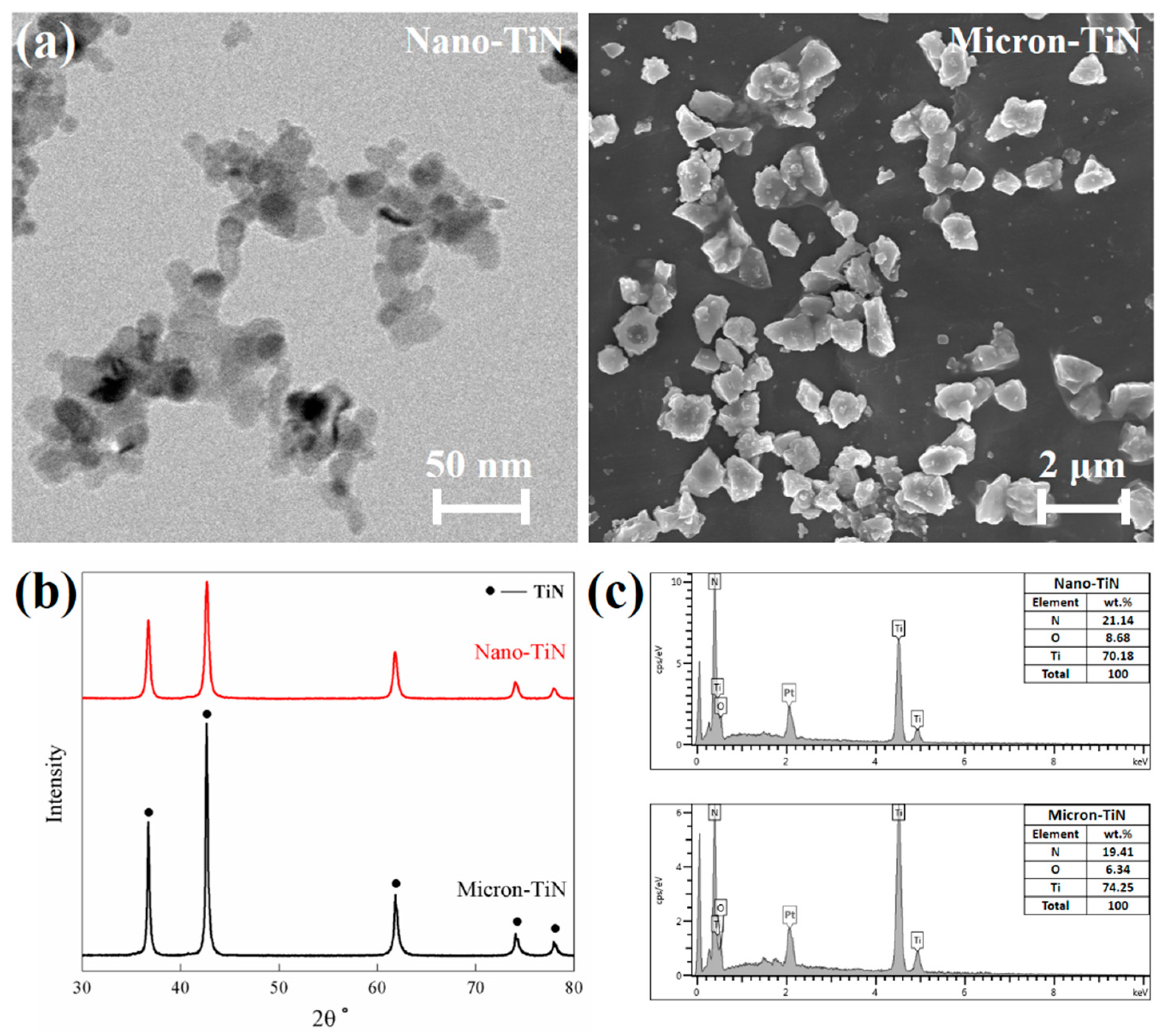
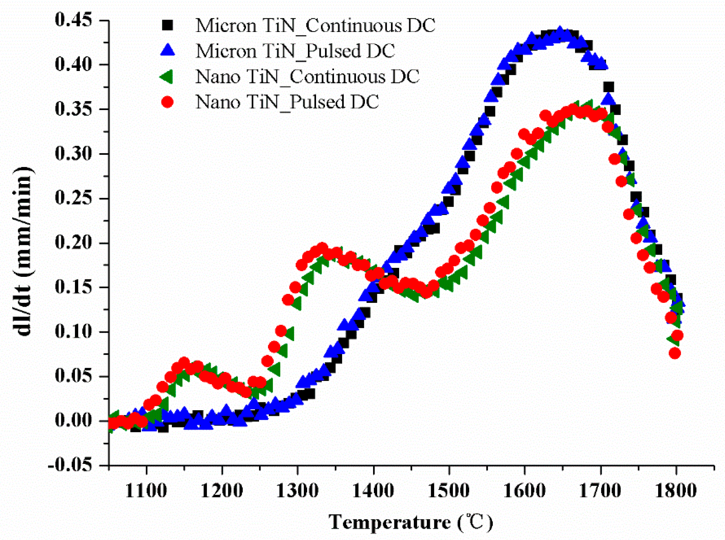
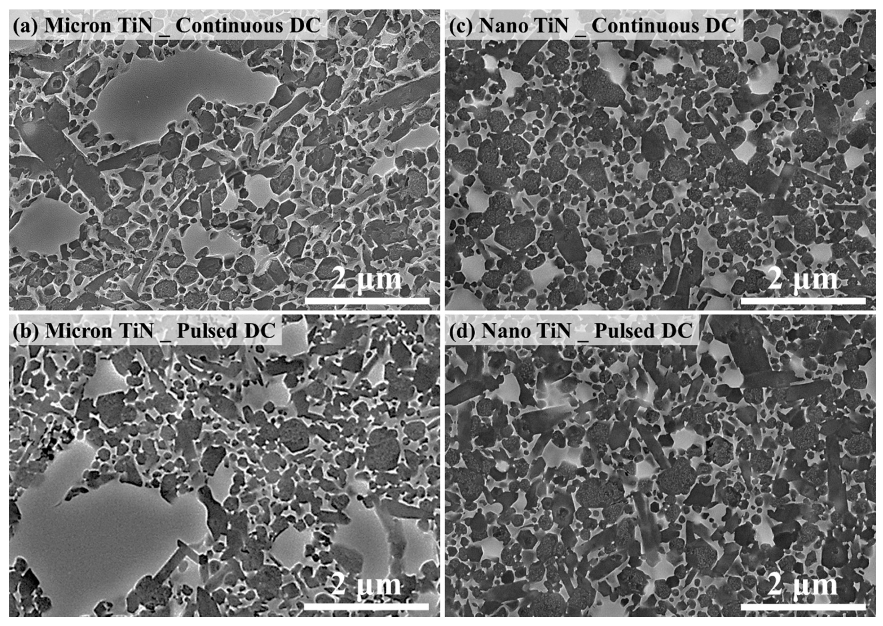
3.1. Scale-Effect of Electric Field-Induced Densification
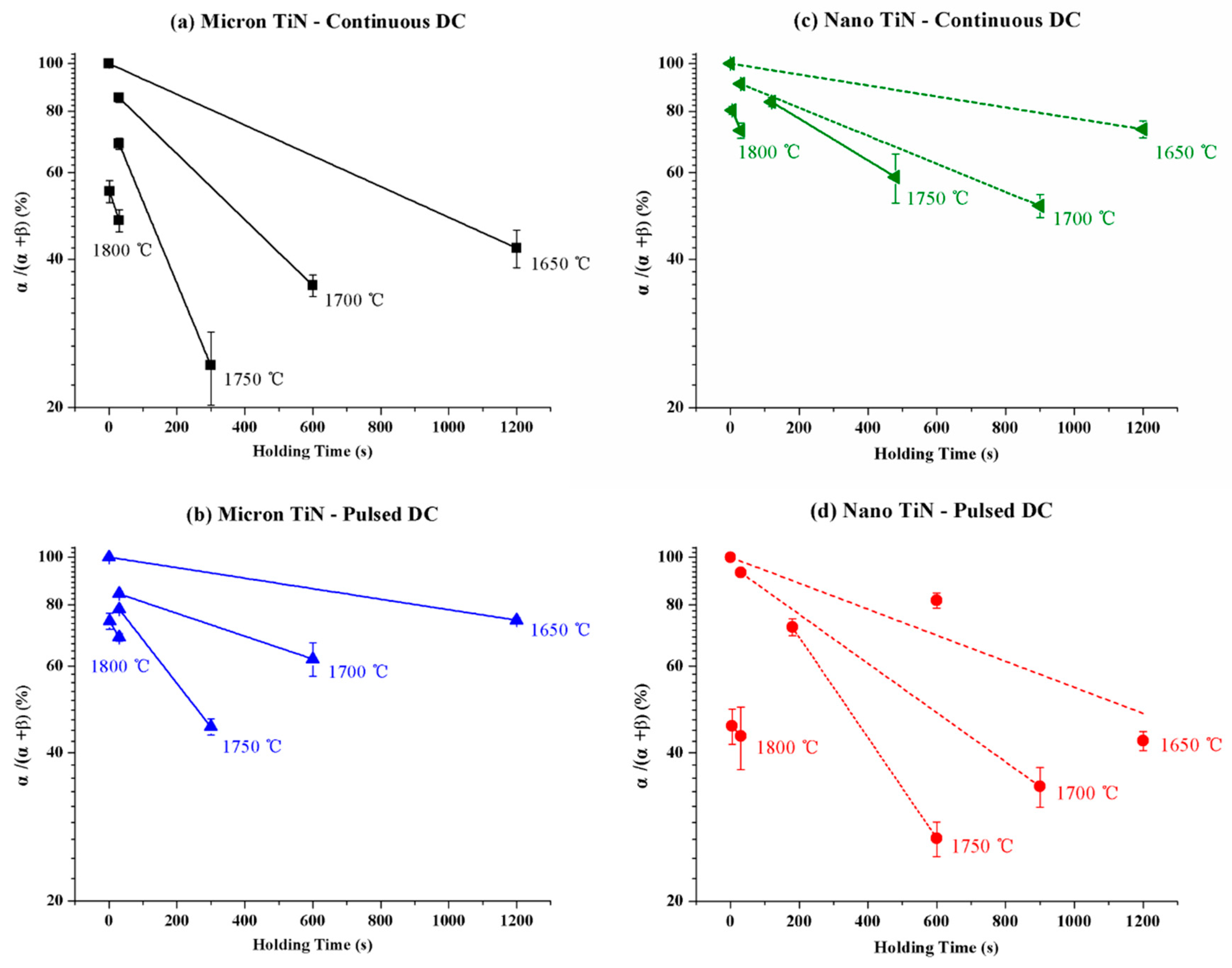
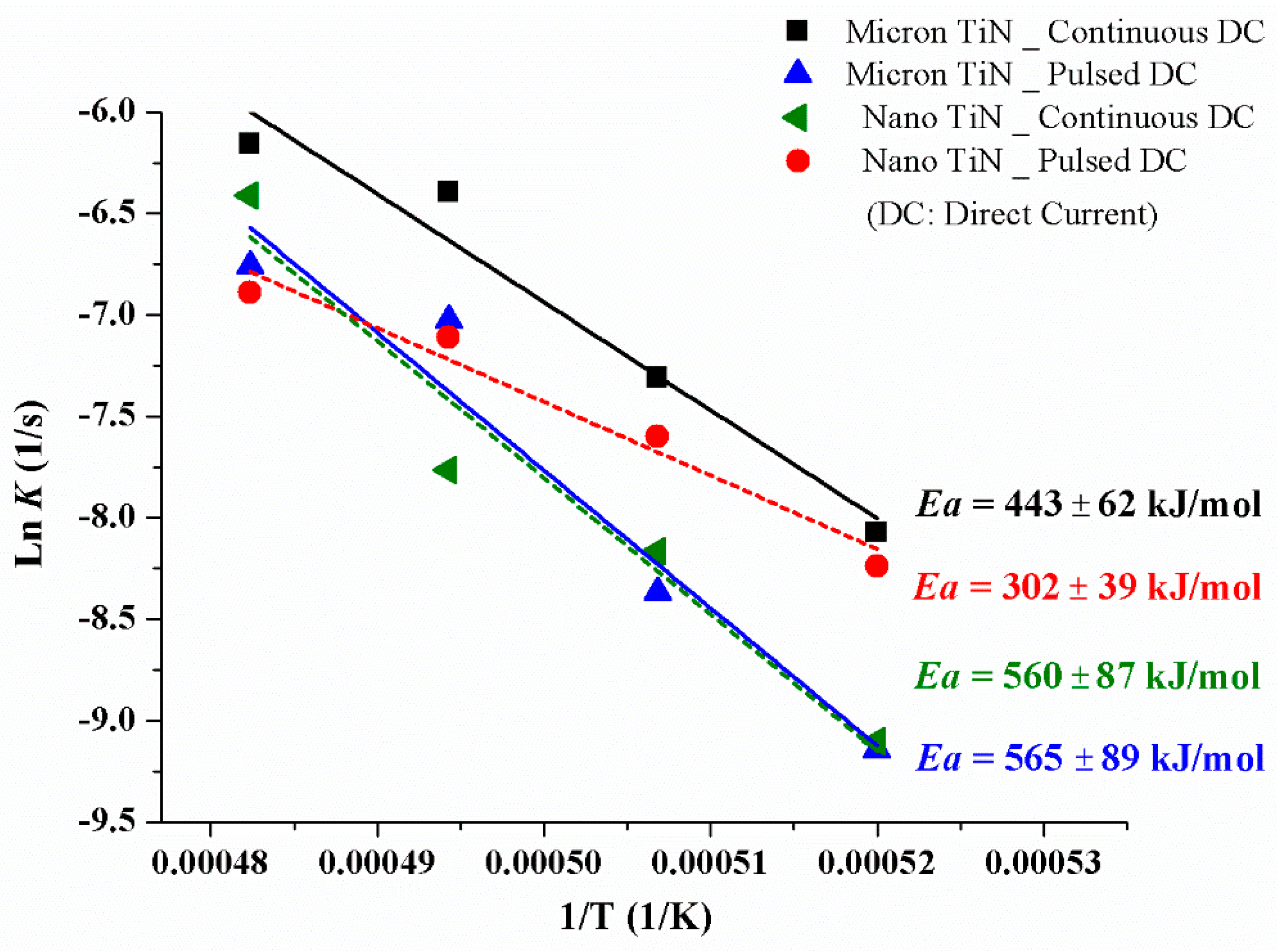
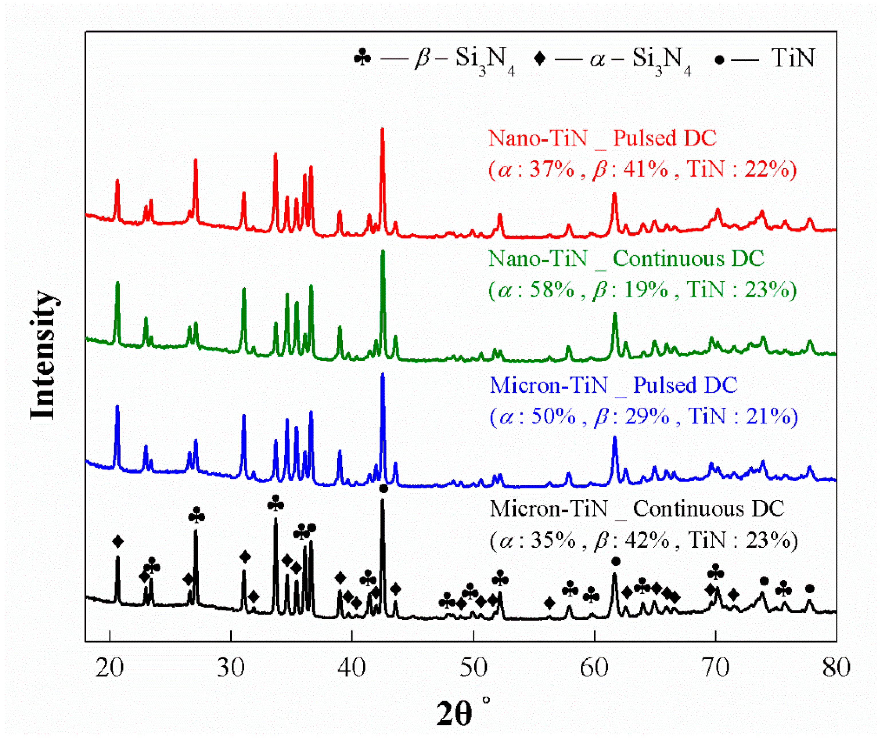
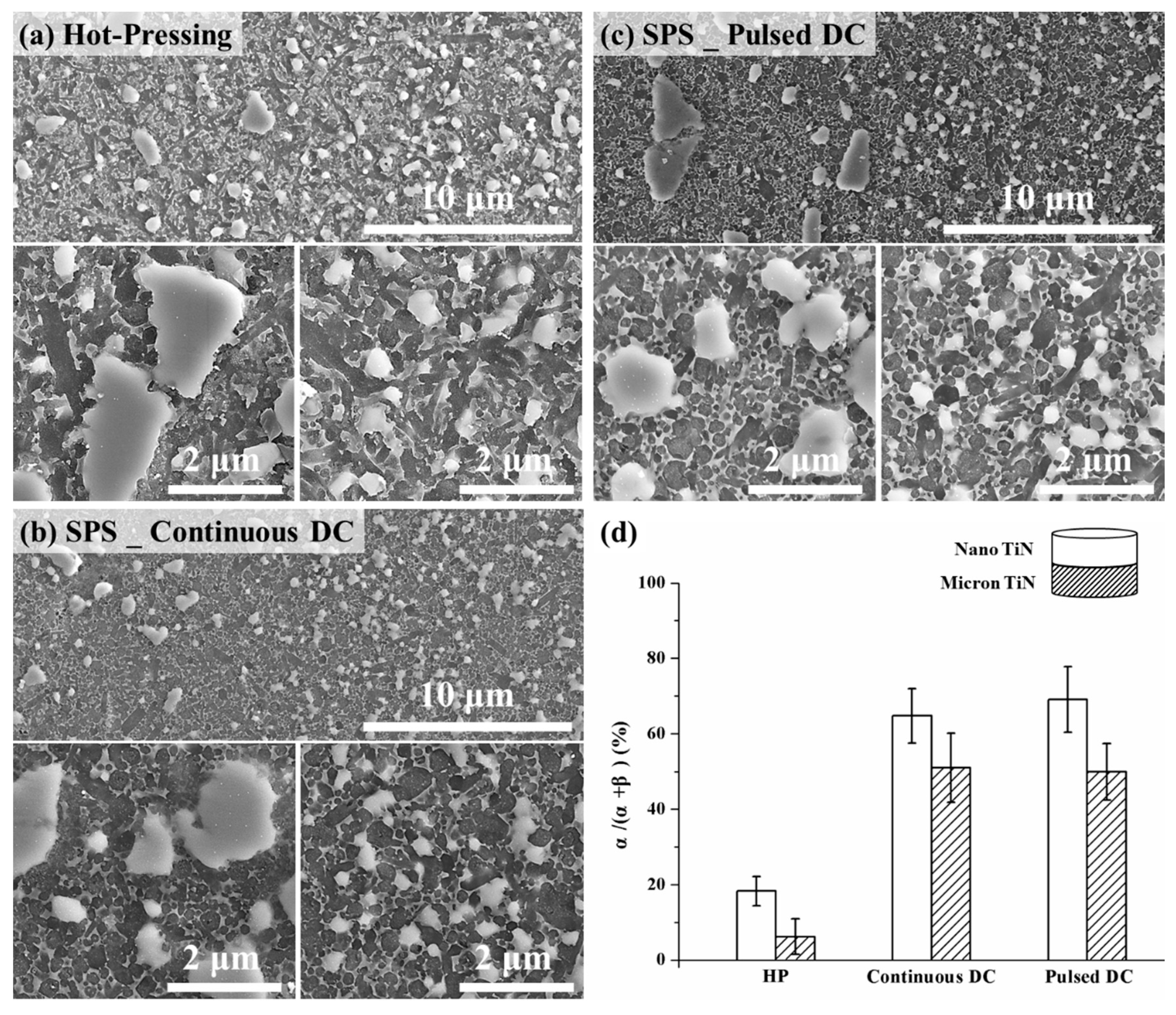
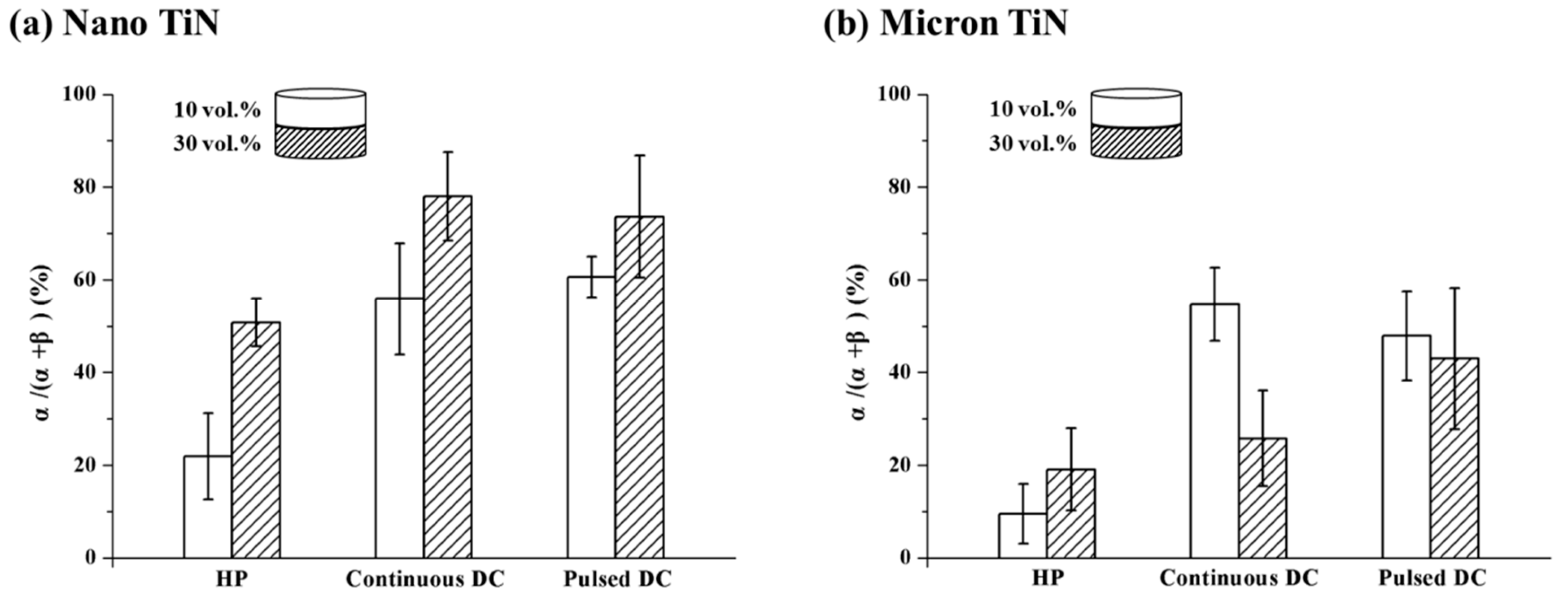
3.2. Scale-Effect of Electric Field-Induced α–β Conversion
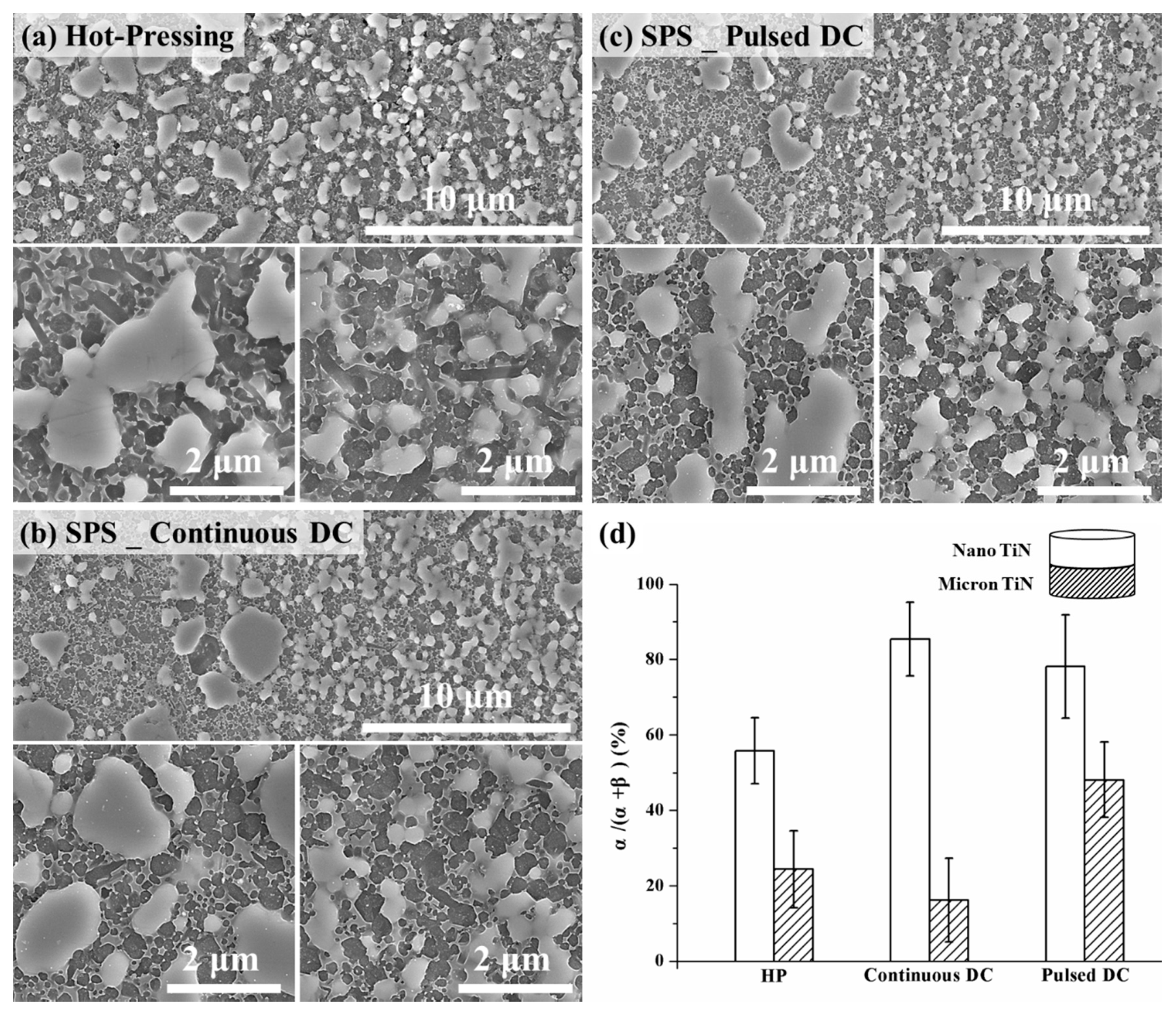
3.3. Design and Fabrication of Multi-Layered Graded Si3N4–TiN Ceramics
4. Conclusions
Author Contributions
Funding
Conflicts of Interest
References
- Lukianova, O.A.; Ivanov, O.N. The effect of Al2O3-MgO additives on the microstructure of spark plasma sintered silicon nitride. Ceram. Int. 2018, 44, 390–393. [Google Scholar] [CrossRef]
- Han, W.; Li, Y.; Chen, G.; Yang, Q. Effect of sintering additive composition on microstructure and mechanical properties of silicon nitride. Mater. Sci. Eng. A 2017, 700, 19–24. [Google Scholar] [CrossRef]
- Zhao, P.; Li, Q.; Yi, R.; Wang, Z.; Lu, L.; Cheng, X.; Dong, S. Fabrication and microstructure of liquid sintered porous SiC ceramics through spark plasma sintering. J. Alloys Compd. 2018, 748, 36–43. [Google Scholar] [CrossRef]
- Kawano, S.; Takahashi, J.; Shimada, S. The preparation and spark plasma sintering of silicon nitride-based materials coated with nano-sized TiN. J. Eur. Ceram. Soc. 2004, 24, 309–312. [Google Scholar] [CrossRef]
- Belmonte, M.; González-Julián, J.; Miranzo, P.; Osendi, M.I. Continuous in situ functionally graded silicon nitride materials. Acta Mater. 2009, 57, 2607–2612. [Google Scholar] [CrossRef]
- Reveron, H.; Blanchard, L.; Vitupier, Y.; Rivière, E.; Bonnefont, G.; Fantozzi, G. Spark Plasma Sintering of fine alpha-silicon nitride ceramics with LAS for spatial applications. J. Eur. Ceram. Soc. 2011, 31, 645–652. [Google Scholar] [CrossRef]
- Bordia, R.K.; Kang, S.J.L.; Olevsky, E.A. Current understanding and future research directions at the onset of the next century of sintering science and technology. J. Am. Ceram. Soc. 2017, 100, 2314–2352. [Google Scholar] [CrossRef]
- Olevsky, E.A.; Kandukuri, S.; Froyen, L. Consolidation enhancement in spark-plasma sintering: Impact of high heating rates. J. Appl. Phys. 2007, 102, 114913. [Google Scholar] [CrossRef]
- Demuynck, M.; Erauw, J.P.O.; Biest, V.D.; Delannay, F.; Cambier, F. Influence of conductive secondary phase on thermal gradients development during Spark Plasma Sintering (SPS) of ceramic composites. Ceram. Int. 2016, 42, 17990–17996. [Google Scholar] [CrossRef]
- Peillon, N.; Zuo, F.; Meunier, C.; Saunier, S.; Marinel, S.; Goeuriot, D. In-situ studies on preparation of ZnAl2O4 spinel using microwave reactive sintering technique. Mater. Lett. 2016, 167, 77–80. [Google Scholar] [CrossRef]
- Zuo, F.; Meng, F.; Lin, D.T.; Lv, J.; Yu, J.J.; Chen, Q.; Wang, H.J.; He, F.P.; Senger, M.; Lin, H.T. Effect of current pattern and conductive phase on sintering behavior of Si3N4-based ceramic composite. Ceram. Int. 2018, 44, 9561–9567. [Google Scholar] [CrossRef]
- Belmonte, M.; González-Julián, J.; Miranzo, P.; Osendi, M.I. Spark plasma sintering: A powerful tool to develop new silicon nitride-based materials. J. Eur. Ceram. Soc. 2010, 30, 2937–2946. [Google Scholar] [CrossRef]
- Yu, J.J.; Guo, W.M.; Wei, W.X.; Lin, H.T.; Wang, C.Y. Fabrication and wear behaviors of graded Si3N4 ceramics by the combination of two-step sintering and β-Si3N4 seeds. J. Eur. Ceram. Soc. 2018, 38, 3457–3462. [Google Scholar] [CrossRef]
- Yu, J.J.; Sun, S.K.; Wei, W.X.; Guo, W.M.; Plucknett, K.; Lin, H.T. Continuous and symmetric graded Si3N4 ceramics designed by spark plasma sintering at 15 MPa. Ceram. Int. 2019, 45, 16703–16706. [Google Scholar] [CrossRef]
- Kitagawa, M.Y.; Wada, S.; Murayama, N. Pulsed electric current sintering of silicon nitride. J. Am. Ceram. Soc. 2003, 86, 387–394. [Google Scholar] [CrossRef]
- Wada, S.; Suganuma, M.; Kitagawa, Y.; Murayama, N. Comparison between pulse electric current sintering and hot pressing of silicon nitride ceramics. J. Ceram. Soc. Jpn. 1999, 107, 887–890. [Google Scholar] [CrossRef]
- Rietveld, H.M. A profile refinement method for nuclear and magnetic structures. J. Appl. Cryst. 1969, 2, 65–71. [Google Scholar] [CrossRef]
- Miranzo, P.; González-Julián, J.; Osendi, M.I.; Belmonte, M. Enhanced particle rearrangement during liquid phase spark plasma sintering of silicon nitride-based ceramics. Ceram. Int. 2011, 37, 159–166. [Google Scholar] [CrossRef]
- Shen, Z.J.; Zhao, Z.; Peng, H.; Nygren, M. Formation of tough interlocking microstructures in silicon nitride ceramics by dynamic ripening. Nature 2002, 417, 266–269. [Google Scholar] [CrossRef]
- Mugele, F.; Baret, J.C. Electrowetting: From basics to applications. J. Phys. Condes. Matter. 2005, 17, R705–R774. [Google Scholar] [CrossRef]
- Bowen, L.J.; Weston, R.J.; Carruthers, T.G.; Brook, R.J. Hot-pressing and the α-β phase transformation in silicon nitride. J. Mater. Sci. 1978, 13, 341–350. [Google Scholar] [CrossRef]
- Bowen, L.J.; Carruthers, T.G.; Brook, R.J. Hot-pressing of Si3N4 with Y2O3 and Li2O as Additives. J. Am. Ceram. Soc. 1978, 61, 335–359. [Google Scholar] [CrossRef]
- Becher, P.F.; Painter, G.S.; Shibata, N.; Waters, S.B.; Lin, H.T. Effects of rare-earth (RE) intergranular adsorption on the phase transformation, microstructure evolution, and mechanical properties in silicon nitride with RE2O3 + MgO additives: RE = La, Gd, and Lu. Am. Ceram. Soc. 2008, 91, 2328–2336. [Google Scholar] [CrossRef]
- Becher, P.F.; Ferber, M.K.; Riester, L.; Waters, M.J.; Hoffmann, S.B.; Satet, R. The Influence of Mg substitution for Al on the properties of SiREMe oxynitride Glasses. J. Non-Cryst. Solids 2004, 333, 124–128. [Google Scholar] [CrossRef]
- Becher, P.F.; Ferber, M.K. The temperature dependent viscosity of SiREAl-based glasses as a function of N:O and RE:Al ratios where RE = La, Gd, Y and Lu. J. Am. Ceram. Soc. 2004, 87, 1274–1279. [Google Scholar] [CrossRef]
- Zuo, F.; Badev, A.; Saunier, S.; Goeuriot, D.; Heuguet, R.; Marinel, S. Microwave versus conventional sintering: Estimate of the apparent activation energy for densification of α-alumina and zinc oxide. J. Eur. Ceram. Soc. 2014, 34, 3103–3110. [Google Scholar] [CrossRef]
- Maniere, C.; Pavia, A.; Durand, L.; Chevallier, G.; Bley, V.; Afanga, K.; Peigney, A.; Estournès, C. Pulse analysis and electric contact measurements in spark plasma sintering. Electr. Power Syst. Res. 2015, 127, 307–313. [Google Scholar] [CrossRef]
- Grasso, S.; Sakka, Y. Electric field in SPS: Geometry and pulsed current effects. J. Ceram. Soc. Jpn. 2013, 121, 524–526. [Google Scholar] [CrossRef]
- Hadad, M.; Blugan, G.; Küble, J.; Rosse, E.; Rohr, L.; Michler, J. Tribological behaviour of Si3N4 and Si3N4–%TiN based composites and multi-layer laminates. Wear 2006, 260, 634–641. [Google Scholar] [CrossRef]
- Gong, F.; Zhao, J.; Li, Z.L.; Sun, J.L.; Ni, X.Y.; Hou, G.M. Design, fabrication and mechanical properties of multidimensional graded ceramic tool materials. Ceram. Int. 2018, 44, 2941–2951. [Google Scholar] [CrossRef]
© 2019 by the authors. Licensee MDPI, Basel, Switzerland. This article is an open access article distributed under the terms and conditions of the Creative Commons Attribution (CC BY) license (http://creativecommons.org/licenses/by/4.0/).
Share and Cite
Lin, D.-T.; Yuan, L.-J.; Zhang, P.-J.; Zuo, F.; Plucknett, K.; Grasso, S.; Wang, H.-J.; Lin, H.-T. Densification and Phase Transformation in Multi-Layered Graded Si3N4–TiN Components Produced by Field-Assisted Sintering. Materials 2019, 12, 2900. https://doi.org/10.3390/ma12182900
Lin D-T, Yuan L-J, Zhang P-J, Zuo F, Plucknett K, Grasso S, Wang H-J, Lin H-T. Densification and Phase Transformation in Multi-Layered Graded Si3N4–TiN Components Produced by Field-Assisted Sintering. Materials. 2019; 12(18):2900. https://doi.org/10.3390/ma12182900
Chicago/Turabian StyleLin, Dong-Tao, Li-Juan Yuan, Peng-Jie Zhang, Fei Zuo, Kevin Plucknett, Salvatore Grasso, Hong-Jian Wang, and Hua-Tay Lin. 2019. "Densification and Phase Transformation in Multi-Layered Graded Si3N4–TiN Components Produced by Field-Assisted Sintering" Materials 12, no. 18: 2900. https://doi.org/10.3390/ma12182900
APA StyleLin, D.-T., Yuan, L.-J., Zhang, P.-J., Zuo, F., Plucknett, K., Grasso, S., Wang, H.-J., & Lin, H.-T. (2019). Densification and Phase Transformation in Multi-Layered Graded Si3N4–TiN Components Produced by Field-Assisted Sintering. Materials, 12(18), 2900. https://doi.org/10.3390/ma12182900


