Article

Modulating Band Gap of Boron Doping in Amorphous Carbon Nano-Film

State Key Laboratory of Superhard Materials, College of Physics, Jilin University, 2699 Qianjin Street, Changchun 130012, China
*
Authors to whom correspondence should be addressed.
Materials 2019, 12(11), 1780; https://doi.org/10.3390/ma12111780
Submission received: 11 May 2019 / Revised: 27 May 2019 / Accepted: 30 May 2019 / Published: 31 May 2019
(This article belongs to the Special Issue Nanocarbon Based Composites)

Abstract

:
Amorphous carbon (a-C) films are attracting considerable attention to due their large optical band gap (Eopt) range of 1–4 eV. But the hopping conducting mechanism of boron doping a-C (a-C:B) is still mysterious. To exploring the intrinsic reasons behind the semiconductor properties of a-C:B, in this work, the boron doping a-C (a-C:B) nano-film was prepared, and the growth rate and Eopt changing were analyzed by controlling the different experimental conditions of magnetron sputtering. A rapid deposition rate of 10.55 nm/min was obtained. The Eopt is reduced from 3.19 eV to 2.78 eV by improving the substrate temperature and sputtering power. The proportion of sp2/sp3 increasing was uncovered with narrowing the Eopt. The shrinking Eopt can be attributed to the fact that boron atoms act as a fluxing agent to promote carbon atoms to form sp2 hybridization at low energy. Furthermore, boron atoms can impede the formation of σ bonds in carbon atom sp3 hybridization by forming B–C bonds with high energy, and induce the sp3 hybridization transfer to sp2 hybridization. This work is significant to further study of amorphous semiconductor films.

Graphical Abstract

1. Introduction

Semiconductor films are the most common form of amorphous carbon (a-C) films, owing to the superior mechanical, optical, and opto-electronic properties [1,2,3,4,5]. Even though the carbon atoms are disordered in a-C, the optical band gap (Eopt) is still controllable, and the Eopt can be changed over a quite large range from 1 eV to 4 eV [6,7]. Thus, the superior properties of a-C arise from adjustable Eopt, which can extend to visible light [8,9]. This is an effective way to adjust the Eopt with doping boron, nitrogen and phosphorus [10], which can form n-type or p-type semiconductors [11,12]. For example, nitrogen/phosphorus incorporate a-C is n-type semiconductor, and Eopt decreases from 2.5 eV to 1.6 eV with increasing nitrogen content [11]. The reason for the change in Eopt is attributed to modifications in the proportion of sp2 and sp3 hybridization [13,14]. A high content of sp3 hybridization can induce diamond-like properties, such as tetrahedral a-C (ta-C) [15], and the sp2 hybridization of a-C can generate graphite-like properties. Carey et al. described a-C as a conductive sp2 phase embedded in electrically insulating sp3 matrix [16]. Furthermore, a-C demonstrates hopping conductivity; hence, a high proportion of sp2 hybridization is preferred to narrow the Eopt [17]. However, the reasons why doping elements interconvert between sp2 and sp3 hybridization are still unclear, and further study to uncover the basis of the semiconductor properties of a-C is required.
Boron has one fewer electrons than carbon, which allows it to generate p-type doping in a-C [7,18]. Boron atoms can release stress with a high sp3 content in boron-incorporated ta-C (ta-C:B) [15,19], and boron atoms can passivate the dangling bonds on the surface of carbon atoms, which can enhance the stability of materials to resist oxidization and corrosion [11]. In general, boron doping in a-C negatively affects conductance due to the presence of boron atoms which are void of π electrons, which is detrimental to sp2 hybridization. Schenk et al. among others found that sp3 hybridization becomes dominated with increasing boron concentration in boron doping hydrogenated a-C film [20]. Nastasi et al. also showed that boron doping can increase sp3 hybridization and C–H bonds in hydrogenated a-C [21]. However, in most cases, the sp3 hybridization decreases with increasing boron content. For example, Tan et al. found that sp3 content decreased from 73.8% to 42.5% with boron concentrate increasing from 0.59% to 6.04% in boron-incorporated a-C (a-C:B) [22]. Meanwhile, Rusop et al. reported that the Eopt of a-C:B was almost unchanged with a boron content below 10%, but that Eopt decreased with higher boron content, i.e., more than 10%, and they considered that the decreased Eopt was not caused by an increased sp2 content [16]. Until now, the means by which doping boron influences the hybridization of carbon atoms in a-C remains a mystery. Further study of a-C:B films is important to discover how to modulate the Eopt of a-C, and to understand the inherent reasons behind the interconverted mechanism of sp2 and sp3 hybridization in a-C:B.
In this work, a-C:B nano-films were prepared by magnetron sputtering. The most superior growth rate was determined to obtain a maximum thickness of 5 μm, and the Eopt was analyzed at a fast growth rate. The interconvert between sp2 and sp3 in a-C:B films were analyzed under different experimental conditions of increasing boron target power, carbon target power, substrate temperature, and working pressure. Finally, a reason for the doping boron atoms inducing to form sp2 hybridization is put forward. This work is significant in the development of new functional amorphous semiconductor films.

2. Experimental

Magnetron Sputtering (JGP450, Shenyang Qihui Vacuum Technology Co., Ltd., Shenyang, China) was used to prepare the a-C:B films. The substrate material was glass, and both the boron and carbon targets were pure to 99.999%. The distance between the substrate and target was 55 mm in all cases. The working gas was Ar. Synthesized films were tested by X-ray photoelectron spectroscopy (XPS using a Surface Science Instruments spectrometer, ESCALAB 250, Thermo Electron Corporation, MA, USA) with a focused Al Kα radiation (1486.6 eV), scanning electron microscopy (SEM, MAGELLAN 400, FEI, Hillsboro, OR, USA). High resolution transmission electron microscopy (HRTEM JSM-2100FS, Tokyo, Japan, equipped with selected area electron diffraction (SAED)) was performed to determine the morphology. Raman spectra were studied on a Renishaw (Shanghai, China) in Via micro-Raman spectrometer at room temperature with a 532 nm laser. The thickness of films was analyzed by atomic-Profiler (Veeco Dektak 150, Veeco, Shanghai, China) to determine the deposition rate. Optical transmittance spectra were measured with a UV-3150 double-beam spectrophotometer (Shimadzu, Japan, Japan) in the range from 300 nm to 900 nm. The Eopt for a-C:B films was obtained via the Tauc relationship, (αhν)2 = c(hν−Eopt), where α is the absorption coefficient, c is a constant, and hν is photon energy [23].

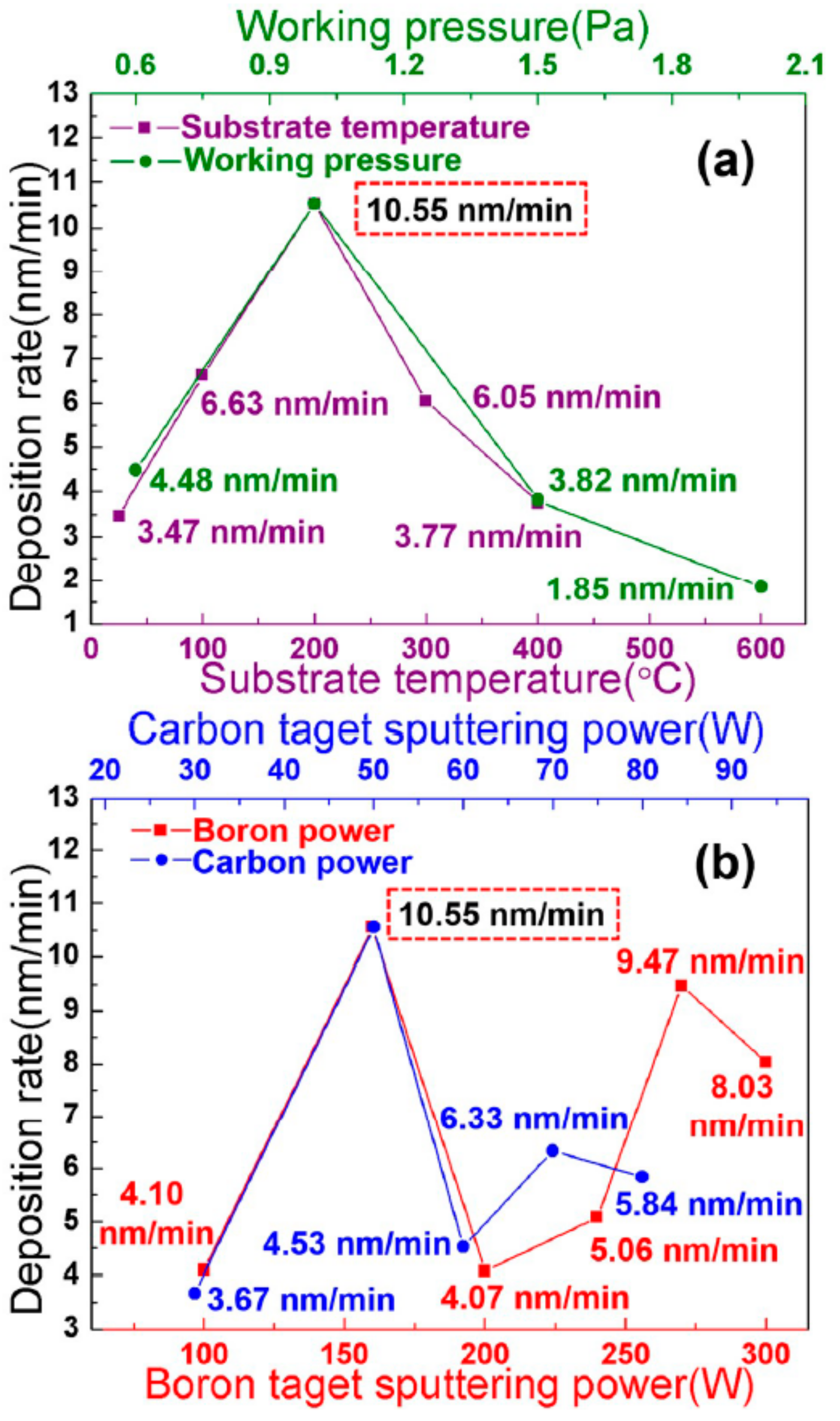
3. Results and Discussion

The deposition rate related to the experimental conditions is shown in Figure 1. The deposition rate of the films increased at first and decreased later with increasing the working pressure or substrate temperature (Figure 1a). The fast deposition rate was 10.55 nm/min at 200 °C and 1.0 Pa. Higher working pressure decreases the mean free path of argon molecules. So, the frequency of the sputtered atoms (boron atoms and carbon atoms) crashing with argon molecules was increased, the emissive power of secondary electrons become stronger, the sputtering capacity also be increased, and thus, the deposition rate was raised. The frequency of sputtered atoms crashing with argon molecules will greatly increase with a working pressure greater than 1.0 Pa, but it is detrimental to the energy of the sputtered atoms due to their dramatic crashes with argon molecules. The quantity of boron and carbon atoms reaching the substrate decreased; thus, the deposition rate decreases with a working pressure higher than 1.0 Pa. In Figure 1a, the reaction rate of boron and carbon atoms is improved with a higher substrate temperature, i.e., of 200 °C, rather than 100 °C. Therefore, the deposition rate increased. Meanwhile, the migration rate of the deposited atoms on the substrate increased when the substrate temperature was higher than 200 °C, which will yield dense films. Hence, the deposition rate decreased with higher substrate temperature, i.e., 200–400 °C; So, a fast deposition rate of 200 °C and 1.0 Pa were chosen in below experiments.
The deposition rate relates to the sputtering power of boron and carbon targets, indicating an undulant curve (Figure 1b). The sputtering rate of boron and carbon atoms will increase with increasing the sputtering power, which may serve to improve the deposition rate. However, by further increasing the sputtering power, the deposition rate decreased to increase the re-sputtering rate of the deposition atoms. Thus, the undulance of the deposition rate at high power may be attributed to the balance of the sputtering rate and the re-sputtering rate of the deposition atoms. The optimum sputtering power for boron is 160 W, and for carbon is 50 W. These settings were chosen in after performing the experiments. The thickness of the film can reach 5 µm with 10 h deposition under optimal conditions.
According to HRTEM results (Figure 2a), the synthesized samples were amorphous. The amorphous nature of the samples was also confirmed by SAED (insert pattern in Figure 2a). The samples are disordered but there was less B2O3 on the surface, which is due to surface oxidation. The morphology of a-C:B films is granulated with a nano size of about 30–80 nm in SEM results (Figure 2b). Thus, the synthesized samples are nano amorphous films.
As synthesized a-C:B was investigated by UV-vis diffuse reflectance spectroscopy, and the Eopt was obtained using the Tauc equation shown in Table 1 and Figure 3. By increasing the working pressure from 1.0 Pa to 2.0 Pa, Eopt reduced from 3.19 eV to 3.08 eV (Table 1, sample 1,5). The reason for this may be the higher pressure, i.e., 2.0 Pa, enhancing the interaction between the boron and carbon atoms. In Table 1, samples 1,6,7, the Eopt reduce just a little (3.19 eV to 3.15 eV) with increasing the temperatures from 200 °C to 400 °C. Thus, temperature may not directly influence the electronic structure, in contrast to changing the content of defect or sp2 cluster size [16]. The Eopt narrowed from 3.19 eV to 2.90 eV (increasing carbon target power, Figure 3a), and from 3.19 eV to 2.78 eV (increasing boron target power, Figure 3b). When the boron target power reached 240 W, sample 3 indicated two Eopt of 2.85 eV and 2.78 eV. In Figure 3b, 3.19 eV, 3.03 eV, and 2.85 eV are compared with 3.19 eV, 3.05 eV, and 2.90 eV in different carbon target powers (Figure 3a). The 2.78 eV may arise from the high boron target power, which indicates that boron atoms have a different state at a power of 240 W. Thus, the target power may be an important factor in modulating the boron and carbon atom combination.
In order to understand the reason behind the Eopt change, the energy states of boron and carbon atoms were analyzed by XPS measurements under the highest deposition rate conditions; only a single condition was changed to study the influence (Table 1, Figure 4). At a lower pressure, i.e., 1.0 Pa, there are no clear B 1s band energy states (Table 1, sample 1); when increasing the pressure to 2.0 Pa, B 1s also does not change (Table 1, sample 5). Because the temperature is low (200 °C) and boron and carbon target powers are just 160 W and 50 W respectively, even with the working pressure increasing to 2.0 Pa, the lower energy can’t induce boron atoms to interact with a-C. But with lower energy (Table 1, sample 1,5), C 1s states can be fitted as four states. The high energy states, 286 eV and 288 eV, are attributable to oxidized carbon (C–O) [11,24], while 284.9 eV arises from C–C σ bonds of sp3 hybridization, which represent the properties of ta-C [14,22]. Meanwhile, the 284.1 eV is due to C=C, which is caused by sp2 hybridization [14,22]. Hence, a-C:B is composed of a sp2 carbon cluster and sp3 carbon matrix. With Raman results, the ID/IG represents a proportion of sp2/sp3 [25], and the ID/IG is not changed with increasing the pressure from 1 to 2 Pa; however, the Eopt is reduced from 3.19 eV to 3.08 eV. The reason for this may be that, although a higher working pressure, i.e., 2.0 Pa, can’t supply enough energy to induce the reaction between boron and carbon atoms, it may shape the size or vary the arrangement of sp2 clusters, which may narrow the hopping distance between two sp2 clusters.
Higher pressure may not directly provide higher energy for a-C:B. Increasing the temperature is effective to improve the reaction energy. As reported, temperature is a crucial factor in modulating the Eopt of a-C by varying defect content and the size of the sp2 cluster [16]. As shown in Table 1, samples 1,6,7, a higher substrate temperature increases the content of sp2, because ID/IG increase from 57% to 61%. This is the reason for the narrowing of the Eopt from 3.19 eV to 3.15 eV. The oxidized boron (191.4 eV) appears at a high temperature, i.e., 300 °C (Table 1, sample 6,7), which is consistent with the HRTEM results of B2O3 on the surface of the samples. Moreover, higher temperatures induce binding energy states at B 1s 189.2 eV and C 1s 283.2 eV, which occurs due to B–C bonds in B4C (Table 1, sample 7) [14]. Thus, higher temperatures facilitate the combination of boron and carbon atoms, and the B–C bonds appear in XPS when the temperature reaches 400 °C. Finally, higher temperatures yield a greater content of sp2 and more B–C bonds.
B–C bonds also appear at a high boron target power, i.e., 240 W (Table 1, sample 3, Figure 4e). High boron target power means high energy with boron atoms, which can promote the reaction between boron and carbon atoms. In XPS, the proportion of C=C and C–C represents the proportion of sp2 and sp3, which relates to the electrical properties [26]. Thus, a higher boron target power can increase the content of sp2 (C=C) (Figure 4b,d,f). And the ID/IG is increased with increasing both boron and carbon target powers (Table 1, sample 1,2,3,4). So, the high target power decreasing the Eopt is due to an increasing in the content of sp2. It is worth mentioning that a higher carbon target power doesn’t generate B–C bonds (Table 1, sample 4). The reason for this may be that high energy carbon atoms only promote the reaction between carbon atoms, and lower boron target power can’t supply enough energy to form B–C bonds. Moreover, this B–C bond may be due to the Eopt of 2.78 eV, as shown in Figure 3b, which indicates that B–C bonds further reduce the Eopt. With these results, the most important factor in the modulation of Eopt in a-C:B is the supplied energy. So, boron atoms can induce the formation of sp2 hybridization in a-C:B with sufficient energy. The narrow Eopt is preferable in a-C films, as reported, and the a-C can be used in solar cells and semiconductors [12]. The narrow Eopt benefits from electron transition, which is related to higher performance. Although the minimum Eopt of this a-C:B is just 2.78 eV, changing the boron and carbon target powers can further modulate the Eopt. Thus, this work is significant for the future development of a-C.
Thus, the narrowing of the Eopt is mainly attributed to the increase in sp2 content. This is consistent with previous reports [22]. However, the content of boron may not the most important factor in the modulation of Eopt, and the supplied energy is the crucial to the generation of sp2 hybridization. We propose the following reasons for this narrowing Eopt: (a) with lower energy, the boron atoms only act on weakly π bonds of sp2 hybridization in carbon atoms; hence, boron atoms can’t react with carbon atoms, and boron atoms act as mixture in a-C:B films. However, the mixture of boron atoms can also serve as a fluxing agent for carbon to form sp2 clusters due to the fact that boron has a lower melting point (about 2075 °C) compared to carbon (3550 °C). Thus, boron atoms can still promote the formation of sp2 clusters with carbon; (b) with higher energy, the boron atoms are able to act on σ bonds in sp3 hybridization to form B–C bonds with terminate edges, and can also induce sp3 hybridization transfer to sp2 hybridization. The intrinsic reason for this is that the π bonds are the weakest, and σ bonds in sp2 hybridization are stronger than σ bonds in sp3 hybridization; thus, boron atoms can influence different carbon bonds with different energies.

4. Conclusions

In this work, variations of Eopt were obtained in a-C:B films. Increasing boron and carbon target powers can increase the sp2 content to narrow the Eopt from 3.19 eV to 2.78 eV. The content of boron may not the most important factor in the modulation of the Eopt, but the supplied energy is crucial in generating sp2 hybridization. So, these results show that boron atoms can act as a fluxing agent to promote the formation of sp2 clusters at lower energy with carbon. Also, boron atoms prefer to act on carbon σ bonds in sp3 hybridization to induce a sp3 hybridization transfer to sp2 hybridization under higher energy. This work is significant to advances the present understanding of a-C and the preparation of new amorphous films.

Author Contributions

Writing—Original Draft Preparation, R.Z., Q.T. and P.Z.; Formal Analysis, R.Z., M.L., X.F., J.L. and M.Y.; Investigation, R.Z., Q.T. and P.Z.; Resources, P.Z.; Data Curation, P.Z.; Writing—Review & Editing, X.W., S.D. and T.C.; Supervision, P.Z.; Project Administration, P.Z.; Funding Acquisition, P.Z.

Funding

This research received funding supports from the China postdoctoral Science Foundation (No. 2016M601374).

Acknowledgments

The authors acknowledge Chaoquan Hu for his technical support in the atomic-Profiler measurements.

Conflicts of Interest

The authors declare no conflict of interest.

References

  1. Myung, H. Synthesis and mechanical properties of amorphous carbon films by closed-field unbalanced magnetron sputtering. Mater. Lett. 2004, 58, 1513–1516. [Google Scholar] [CrossRef]
  2. Rusop, M.; Rusop, M.; Subban, R.Y.; Kamarulzaman, N.; Wui, W.T. Amorphous Carbon Based Solar Cell: Fabrication and Characterization. AIP Conf. Proc. 2010, 1217, 385–390. [Google Scholar] [CrossRef]
  3. Zhai, Z.; Shen, H.; Chen, J. Fast growth of conductive amorphous carbon films by HFCVD with filament temperature control. Mater. Lett. 2018, 228, 293–296. [Google Scholar] [CrossRef]
  4. Sun, Y.; Wu, H.; Li, M.; Meng, Q.; Gao, K.; Lu, X.; Liu, B. The Effect of ZrO2 Nanoparticles on the Microstructure and Properties of Sintered WC-Bronze-Based Diamond Composites. Materials 2016, 9, 343. [Google Scholar] [CrossRef]
  5. Baker, P.A.; Catledge, S.A.; Harris, S.B.; Ham, K.J.; Chen, W.C.; Chen, C.C.; Vohra, Y.K. Computational Predictions and Microwave Plasma Synthesis of Superhard Boron-Carbon Materials. Materials 2018, 11, 1279. [Google Scholar] [CrossRef] [PubMed]
  6. Khan, R.U.A.; Grambole, D.; Silva, S.R.P. Studies of carbon ion self-implantation into hydrogenated amorphous carbon films. Diam. Relat. Mater. 2000, 9, 675–679. [Google Scholar] [CrossRef]
  7. Theye, M.-L.; Paret, V. Spatial organization of the sp2-hybridized carbon atoms and electronic density of states of hydrogenated amorphous carbon films. Carbon 2002, 40, 1153–1166. [Google Scholar] [CrossRef]
  8. Pradhan, D.; Sharon, M. Opto-electrical properties of amorphous carbon thin film deposited from natural precursor camphor. Appl. Surf. Sci. 2007, 253, 7004–7010. [Google Scholar] [CrossRef]
  9. Rusop, M.; Omer, A.M.M.; Adhikari, S.; Adhikary, S.; Uchida, H.; Soga, T.; Jimbo, T.; Umeno, M. The Optical Characteristics Of Nitrogen-Doped Amorphous Carbon Thin-Films Grown On Novel Heat Tolerant Flexible Plastic Substrates By A Newly Developed Microwave Surface Wave Plasma Chemical Vapor Deposition Method. Surf. Rev. Lett. 2004, 11, 585–589. [Google Scholar] [CrossRef]
  10. Baker, P.A.; Goodloe, D.R.; Vohra, Y.K. Morphological Transition in Diamond Thin-Films Induced by Boron in a Microwave Plasma Deposition Process. Materials 2017, 10, 1305. [Google Scholar] [CrossRef] [PubMed]
  11. Yu, Y.H.; Chen, Z.Y.; Luo, E.Z.; Cheung, W.Y.; Zhao, J.P.; Wang, X.; Xu, J.B.; Wong, S.P.; Wilson, I.H. Optical and electrical properties of nitrogen incorporated amorphous carbon films. J. Appl. Phys. 2000, 87, 2874–2879. [Google Scholar] [CrossRef]
  12. Podder, J.; Rusop, M.; Soga, T.; Jimbo, T. Boron doped amorphous carbon thin films grown by r.f. PECVD under different partial pressure. Diam. Relat. Mater. 2005, 14, 1799–1804. [Google Scholar] [CrossRef]
  13. Ronning, C.; Griesmeier, U.; Gross, M.; Hofsgss, H.C.; Downing, R.G.; Lamaze, G.P. Conduction processes in boron- and nitrogen-doped diamond-like carbon films prepared by mass-separated ion beam deposition. Diam. Relat. Mater. 1995, 4, 666–672. [Google Scholar] [CrossRef]
  14. Tan, M.; Zhu, J.; Han, J.; Gao, W.; Niu, L.; Lu, J. Chemical analysis and vibrational properties of boronated tetrahedral amorphous carbon films. Diam. Relat. Mater. 2007, 16, 1739–1745. [Google Scholar] [CrossRef]
  15. Chhowalla, M.; Yin, Y.; Amaratunga, G.A.J.; McKenzie, D.R.; Frauenheim, T. Highly tetrahedral amorphous carbon films with low stress. Appl. Phys. Lett. 1996, 69, 2344–2346. [Google Scholar] [CrossRef]
  16. Carey, J.D.; Silva, S.R.P. Disorder, clustering, and localization effects in amorphous carbon. Phys. Rev. B 2004, 70, 235417. [Google Scholar] [CrossRef] [Green Version]
  17. Vishwakarma, P.N.; Subramanyam, S.V. Hopping conduction in boron doped amorphous carbon films. J. Appl. Phys. 2006, 100, 113702. [Google Scholar] [CrossRef]
  18. Tian, X.M.; Rusop, M.; Hayashi, Y.; Soga, T.; Jimbo, T.; Umeno, M. Photovoltaic characteristics of boron doped amorphous carbon films deposited by pulsed laser deposition using graphite target. Mol. Cryst. Liq. Cryst. 2002, 386, 73–80. [Google Scholar] [CrossRef]
  19. Tan, M.; Zhu, J.; Han, J.; Han, X.; Niu, L.; Chen, W. Stress evolution of tetrahedral amorphous carbon upon boron incorporation. Scr. Mater. 2007, 57, 141–144. [Google Scholar] [CrossRef]
  20. Schenk, A.; Winter, B.; Lutterloh, C.; Biener, J.; Schubert, U.A.; Küppers, J. The influence of boron doping on the structure and thermal decomposition of ultrathin C/B:H films. J. Appl. Phys. 1995, 77, 6006–6014. [Google Scholar] [CrossRef]
  21. He., X.-M.; Walter., K.C.; Nastasi, M. Plasma-immersion ion-processed boron-doped diamond-like carbon films. J. Phys. Condens. Matter 2000, 12, L183–L189. [Google Scholar]
  22. Tan, M.; Zhu, J.; Han, J.; Niu, L.; Lu, J.; Chen, W. Relative fraction of sp3 bonding in boron incorporated amorphous carbon films determined by X-ray photoelectron spectroscopy. Mater. Res. Bull. 2008, 43, 1670–1678. [Google Scholar] [CrossRef]
  23. Morales-Acevedo, A. Effective absorption coefficient for graded band-gap semiconductors and the expected photocurrent density in solar cells. Sol. Energy Mater. Sol. Cells 2009, 93, 41–44. [Google Scholar] [CrossRef]
  24. Merel, P.; Tabbal, M.; Chaker, M.; Moisa, S.; Margot, J. Direct evaluation of the sp3 content in diamond-like-carbon films by XPS. Appl. Surf. Sci. 1998, 136, 105–110. [Google Scholar] [CrossRef]
  25. Cao, H.; Qi, F.; Ouyang, X.; Zhao, N.; Zhou, Y.; Li, B.; Luo, W.; Liao, B.; Luo, J. Effect of Ti Transition Layer Thickness on the Structure, Mechanical and Adhesion Properties of Ti-DLC Coatings on Aluminum Alloys. Materials 2018, 11, 1742. [Google Scholar] [CrossRef] [PubMed]
  26. Popescu, A.; Stan, G.; Duta, L.; Nita, C.; Popescu, C.; Surdu, V.-A.; Husanu, M.-A.; Bita, B.; Ghisleni, R.; Himcinschi, C.; et al. The Role of Ambient Gas and Pressure on the Structuring of Hard Diamond-Like Carbon Films Synthesized by Pulsed Laser Deposition. Materials 2015, 8, 3284–3305. [Google Scholar] [CrossRef]
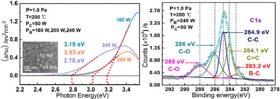
 [Green Version]
Figure 1. The deposition rate patterns; (a) is the deposition rate relates to substrate temperature (purple) and working pressure (green); (b) is the deposition rate relates to boron target power (red) and carbon target power (blue). The rate is 10.55 nm/min with optimal conditions, i.e., 200 °C, 1.0 Pa, boron power 160 W, and carbon power 50 W.
Materials 12 01780 g001
Figure 2. The microstructure and morphology of a-C:B (200 °C, 1.0 Pa, boron target power 200 W, and carbon target power 50 W). (a) is a high resolution transmission electron microscopy (HRTEM) pattern; the inset pattern in (a) is the selected area electron diffraction (SAED) results. (b) is a scanning electron microscopy (SEM) pattern. HRTEM and SAED indicate a-C:B is amorphous; there is B2O3 on the surface of a-C:B. SEM pattern, indicating that a-C:B is granulated with a nano size of about 30–80 nm.
Materials 12 01780 g002
Figure 3. The optical band gap (Eopt) pattern of a-C:B. (a) Eopt relates to different carbon target power; Eopt decreases with increasing carbon target power. (b) Eopt relates to different boron target power; the Eopt decreases with increasing boron target power.
Materials 12 01780 g003
Figure 4. X-ray photoelectron spectroscopy (XPS) patterns relate to different boron target power. All samples are synthesized under the same conditions, i.e., 200 °C, 1.0 Pa, and carbon target power of 50 W. (a,b) are XPS results under boron target power of 160 W. (c,d) are XPS results under boron target power of 200 W. (e,f) are XPS results under boron target power of 240 W. (a,c,e) are the boron 1s state. (b,d,f) are the carbon 1s state. With increasing boron target power to 200 W, B–O bonds appear; with increasing boron target power to 240 W, B–C bonds appear; the C–C peak is decreased and C=C is increased with increasing the boron target power.
Materials 12 01780 g004
Table 1. Synthesis parameters and tested results of samples. All target-substrate distances and deposition times were 55 nm and 30 min respectively; boron target power (PB), the unit is W; carbon target power (PC), the unit is W; substrate temperature (T), the unit is °C; the XPS peak position of binding energy are represent by B–O, C–O, C–C, C=C, B–C, the unit is eV; Eopt is the optical band gap, the unit is eV; ID/IG is the proportion of D and G modes in the Raman results.
SamplePBPCTPaB–OC–O C=CC–C B–CEoptID/IG
1160502001.0-286; 288284.1284.9-3.1957%
2200502001.0191.4286; 287.8284.1284.9-3.0359%
3240502001.0191.3286; 288284.1284.9189.2; 283.22.7861%
4160802001.0191.3286; 288284.1284.9-2.9064%
5160502002.0-286.2; 288.2284.1284.9-3.0857%
6160503001.0191.4286; 288284.1284.9189.2; 283.23.1659%
7160504001.0191.2286; 288284.1284.9189.2; 283.23.1561%

