Enhancing Photovoltaic Performance of Plasmonic Silicon Solar Cells with ITO Nanoparticles Dispersed in SiO2 Anti-Reflective Layer


Abstract
1. Introduction
2. Experimental Methods
2.1. Characterization of Optical Properties and Surface Morphology of the ITO Nanoparticles Dispersed in a SiO2 Layer
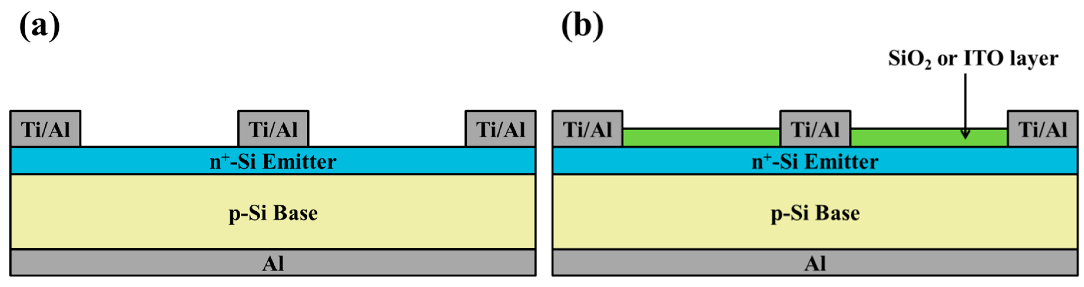
2.2. Fabrication and Characterization of Bare Silicon Solar Cells and Cells Coated with an Anti-Reflective Layer of SiO2 or ITO
2.3. Fabrication And Characterization of Plasmonic Silicon Solar Cells with ITO-NPs Dispersed in SiO2 ARC
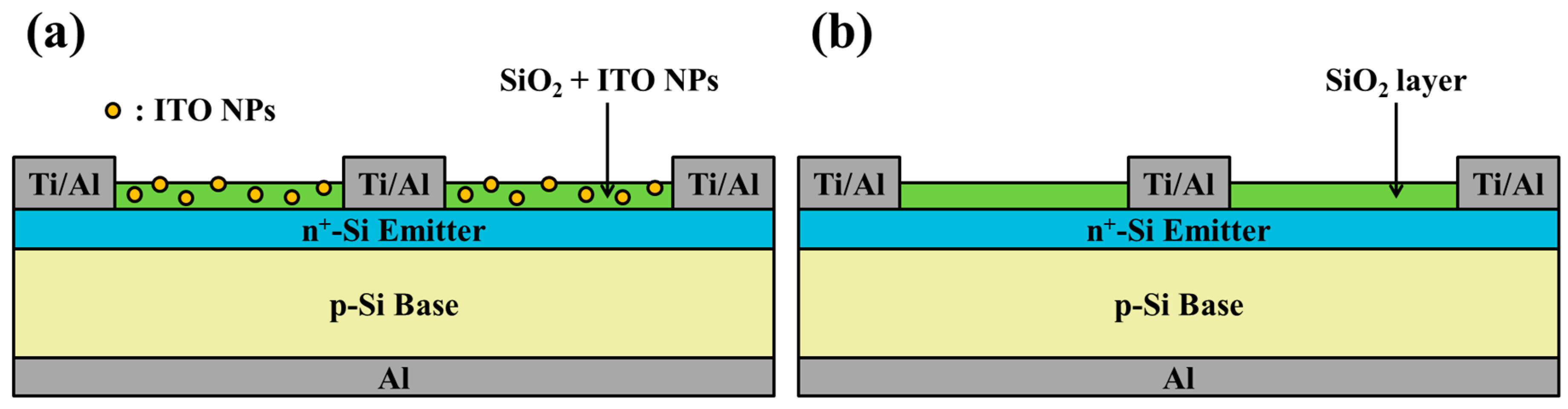
2.3.1. SiO2 ARC with Dispersed ITO Nanoparticles
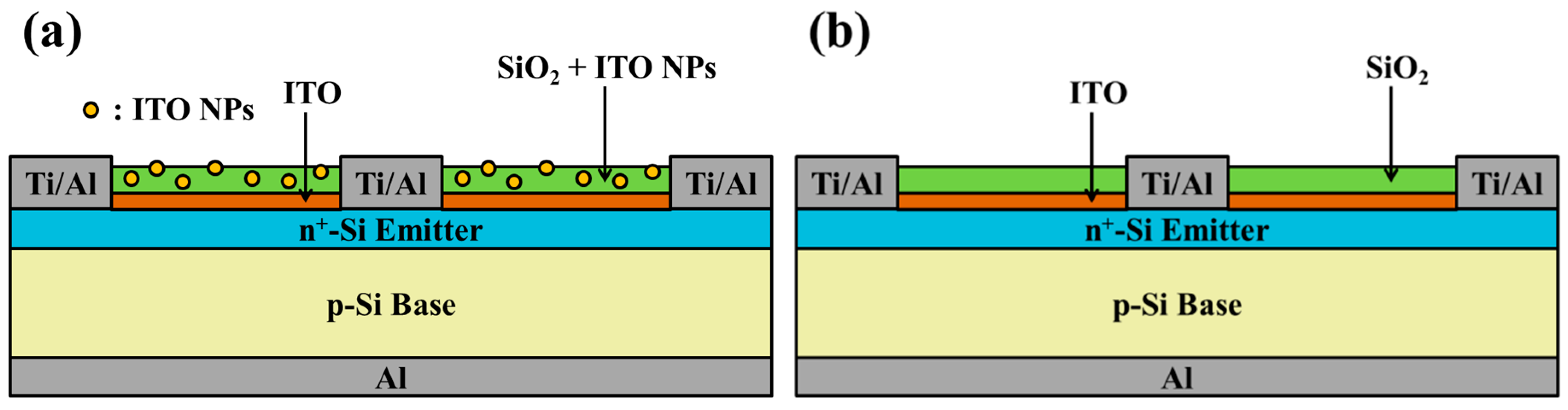
2.3.2. Compound ITO/SiO2 ARC Comprising ITO Nanoparticles Dispersed in SiO2 Layer
3. Results and Discussion
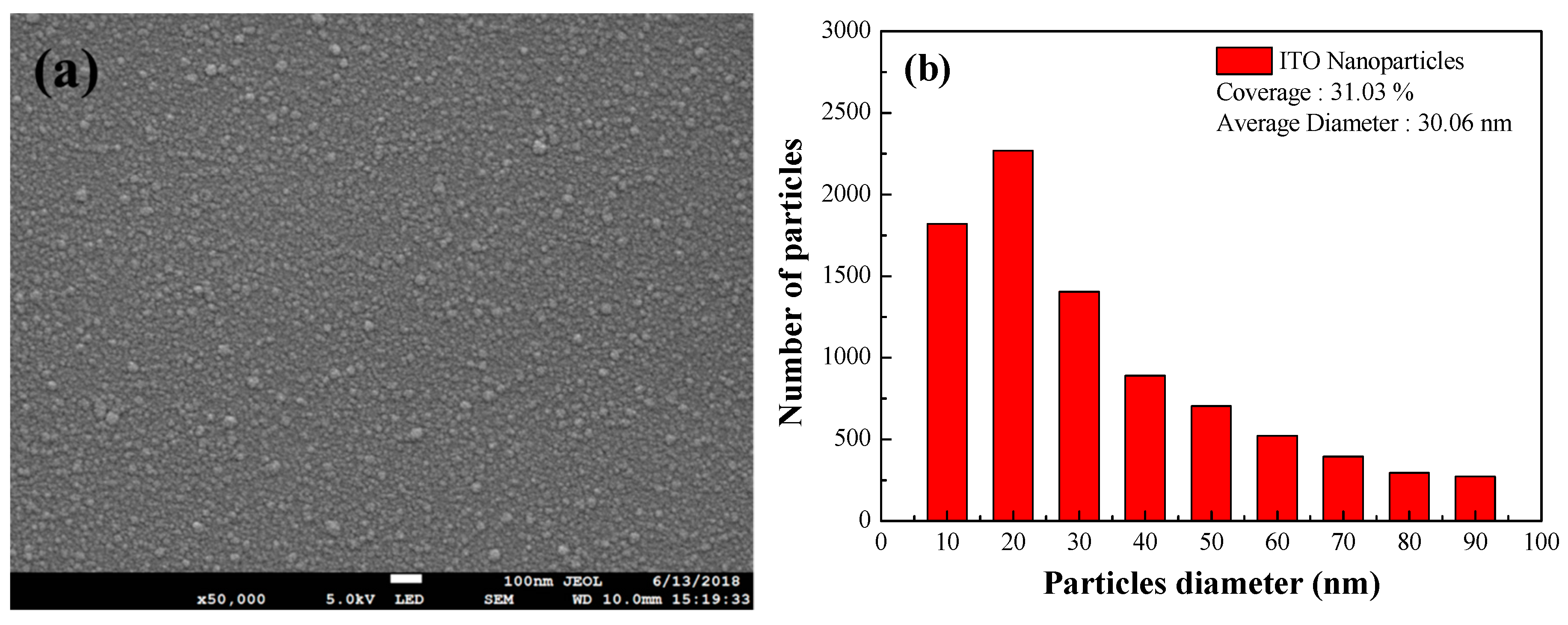
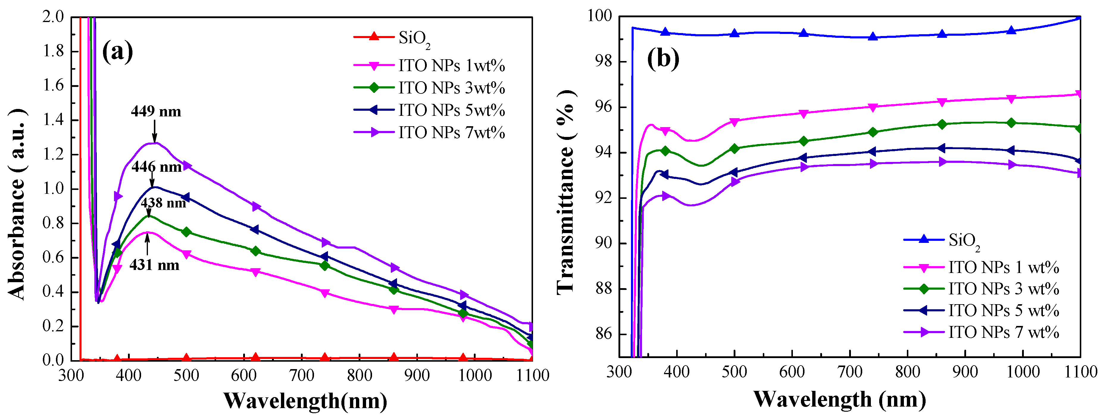
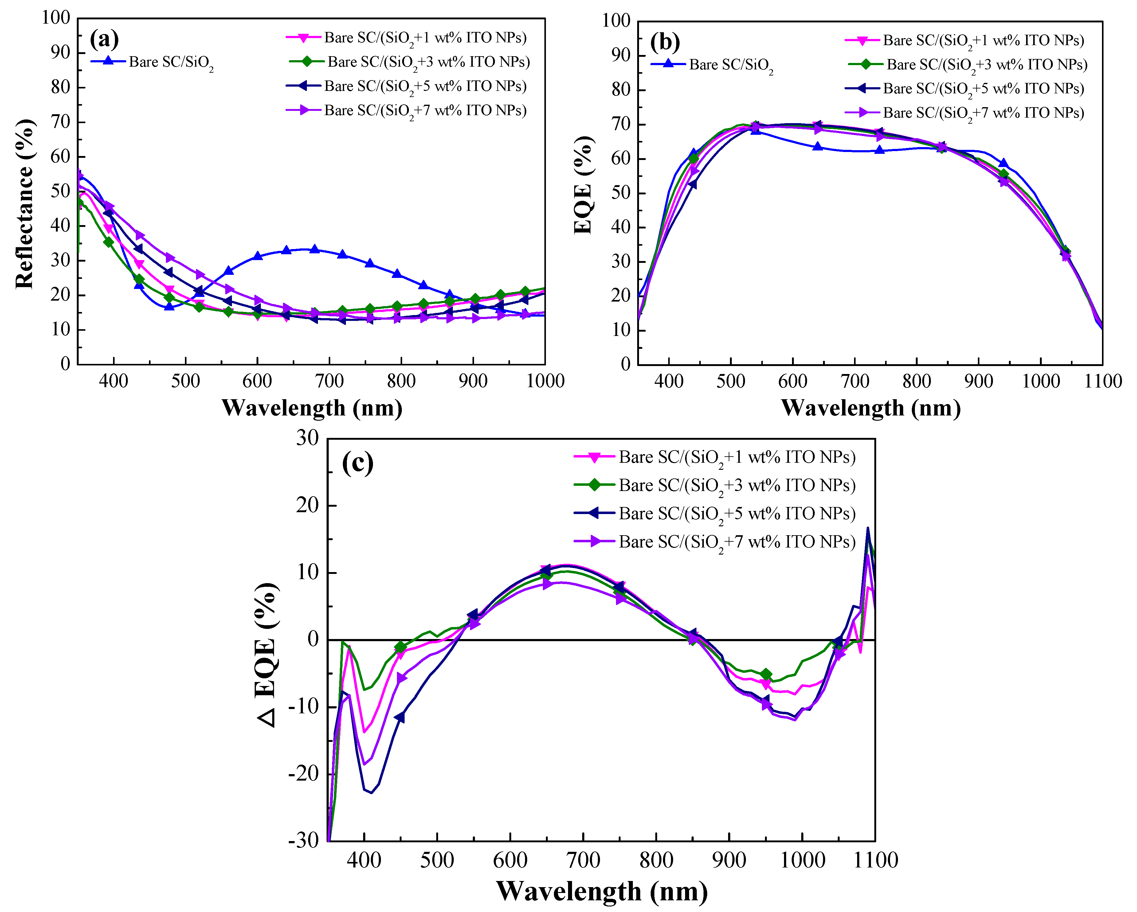
3.1. The Surface Morphology and Optical Properties of the ITO Nanoparticles Dispersed in SiO2 Layer
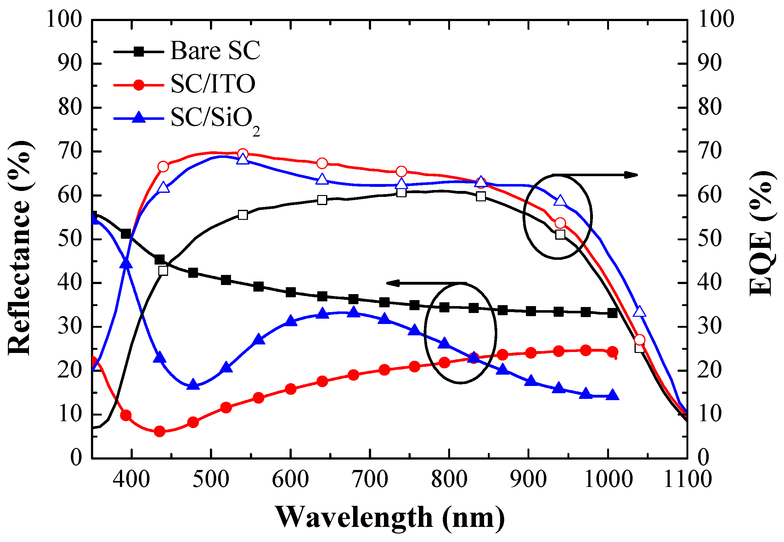
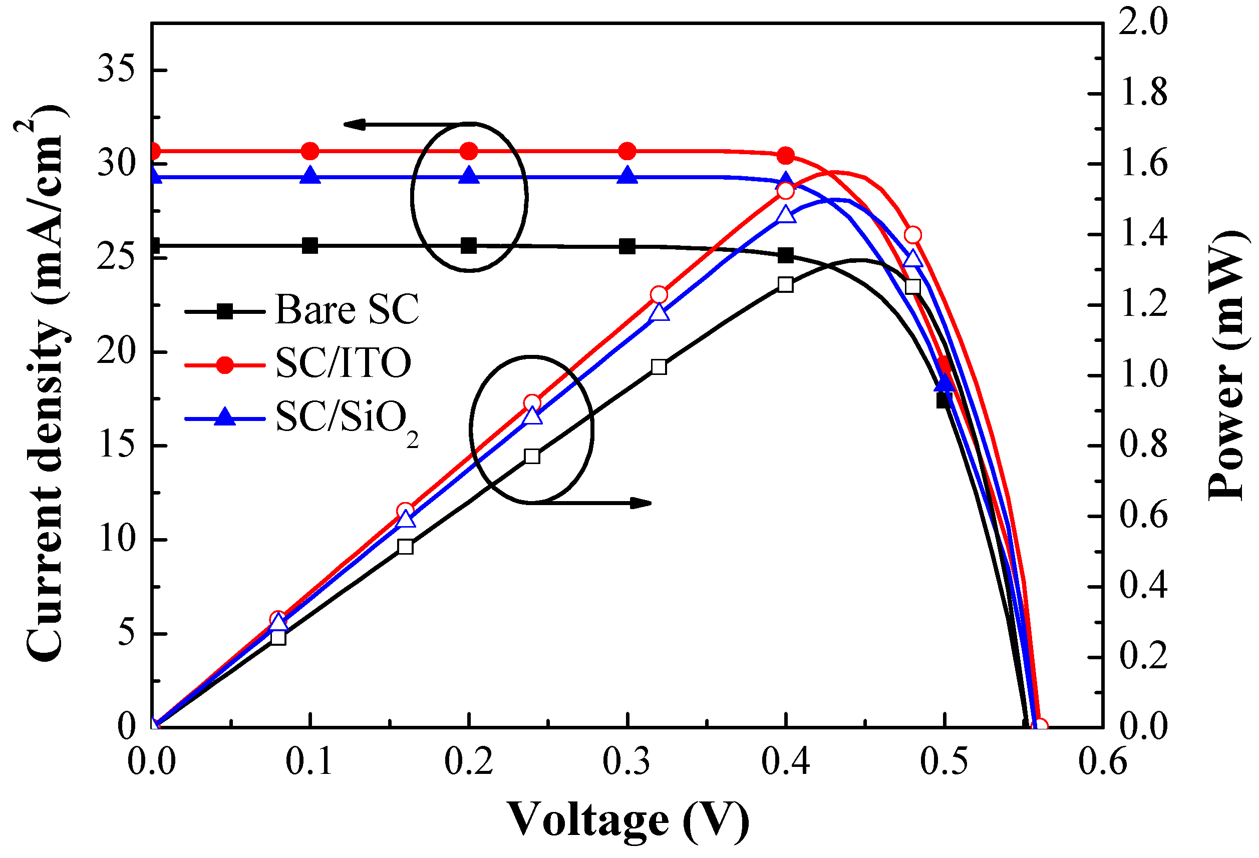
3.2. Characterization of Cells Coated with an Anti-Reflective Layer of SiO2 or ITO
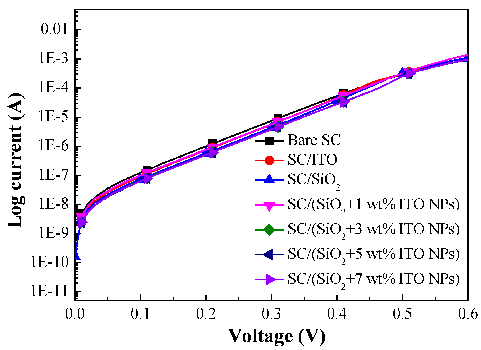
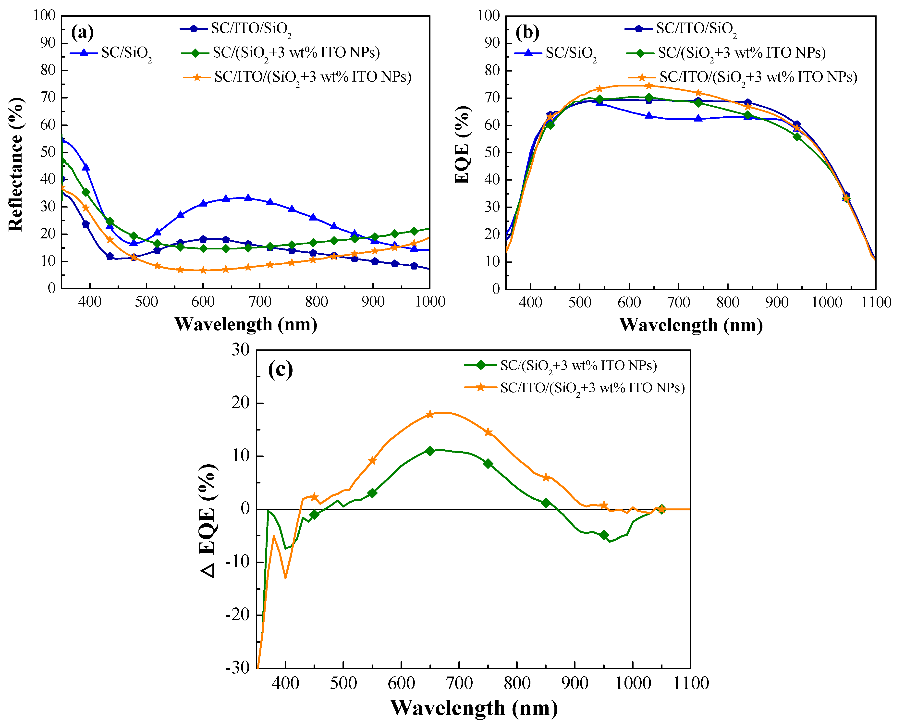
3.3. Characterization of Silicon Solar Cells Coated with Compound ITO/SiO2 ARC Comprising ITO-NPs Dispersed in SiO2 Layer
4. Conclusions
Author Contributions
Funding
Conflicts of Interest
References
- Araújo, A.; Mendes, M.J.; Mateus, T.; Costa, J.; Nunes, D.; Fortunato, E.; Águas, H.; Martins, R. Ultra-fast plasmonic back reflectors production for light trapping in thin Si solar cells. Sol. Energy 2018, 174, 786–792. [Google Scholar] [CrossRef]
- Veenkamp, R.J.; Ye, W.N. Plasmonic metal nanocubes for broadband light absorption enhancement in thin-film a-Si solar cells. J. Appl. Phys. 2014, 115, 124317. [Google Scholar] [CrossRef]
- Beck, F.J.; Mokkapati, S.; Catchpole, K.R. Plasmonic light-trapping for Si solar cells using self-assembled, Ag nanoparticles. Prog. Photovolt: Res. Appl. 2010, 18, 500–504. [Google Scholar] [CrossRef]
- Catchpole, K.R.; Polman, A. Design principles for particle plasmon enhanced solar cells. Appl. Phys. Lett. 2008, 93, 191113. [Google Scholar] [CrossRef]
- Atwater, H.A.; Polman, A. Plasmonics for improved photovoltaic devices. Nat. Mater. 2010, 9, 205–213. [Google Scholar] [CrossRef]
- Garcia, M.A. Surface plasmons in metallic nanoparticles: fundamentals and applications. J. Phys. D Appl. Phys. 2011, 44, 283001. [Google Scholar] [CrossRef]
- Kelly, K.L.; Coronado, E.; Zhao, L.L.; Schatz, G.C. The optical properties of metal nanoparticles: the influence of size, shape, and dielectric environment. J. Phys. Chem. B 2003, 107, 668–677. [Google Scholar] [CrossRef]
- Derkacs, D.; Lim, S.H.; Matheu, P.; Mar, W.; Yu, E.T. Improved performance of amorphous silicon solar cells via scattering from surface plasmon polaritons in nearby metallic nanoparticles. Appl. Phys. Lett. 2006, 89, 093103. [Google Scholar] [CrossRef]
- Pedrueza, E.; Sancho-Parramon, J.; Bosch, S.; Valdés, J.L.; Martinez-Pastor, J.P. Plasmonic layers based on Au-nanoparticle-doped TiO2 for optoelectronics: structural and optical properties. Nanotechnology 2013, 24, 065202. [Google Scholar] [CrossRef] [PubMed]
- Sharma, M.; Pudasaini, P.R.; Ruiz-Zepeda, F.; Vinogradova, E.; Ayon, A.A. Plasmonic effects of Au/Ag bimetallic multispiked nanoparticles for photovoltaic applications. ACS Appl. Mater. Interfaces 2014, 6, 15472–15479. [Google Scholar] [CrossRef]
- Tan, H.; Santbergen, R.; Yang, G.; Smets, A.H.M.; Zeman, M. Combined optical and electrical design of plasmonic back reflector for high-efficiency thin-film silicon solar cells. IEEE J. Photovolt. 2013, 3, 53–58. [Google Scholar] [CrossRef]
- Tong, C.; Yun, J.; Song, H.; Gan, Q.; Anderson, W.A. Plasmonic-enhanced Si schottky barrier solar cells. Sol. Energy Mater. Sol. Cells 2014, 120, 591–595. [Google Scholar] [CrossRef]
- Lesina, A.C.; Paternoster, G.; Mattedi, F.; Ferrario, L.; Berini, P.; Ramunno, L.; Paris, A.; Vaccari, A.; Calliari, L. Modeling and characterization of antireflection coatings with embedded silver nanoparticles for silicon solar cells. Plasmonics 2015, 10, 1525–1536. [Google Scholar] [CrossRef]
- Manai, L.; Rezgui, B.D.; Zaghouani, R.B.; Barakel, D.; Torchio, P.; Palais, O.; Bessais, B. Tuning of light trapping and surface plasmon resonance in silver nanoparticles/c-Si structures for solar cells. Plasmonics 2016, 11, 1273–1277. [Google Scholar] [CrossRef]
- Hylton, N.P.; Li, X.F.; Giannini, V.; Lee, K.-H.; Ekins-Daukes, N.J.; Loo, J.; Vercruysse, D.; Van Dorpe, P.; Sodabanlu, H.; Sugiyama, M.; Maier, S.A. Loss mitigation in plasmonic solar cells: aluminium nanoparticles for broadband photocurrent enhancements in GaAs photodiodes. Sci Rep. 2013, 3, 2874. [Google Scholar] [CrossRef] [PubMed]
- Fantoni, A.; Fernandes, M.; Vygranenko, Y.; Louro, P.; Vieira, M. Visible range plasmonic effect produced by aluminium nanoparticles embedded in amorphous silicon. Phys. Status Solidi C 2015, 12, 1349–1354. [Google Scholar] [CrossRef]
- Parashar, P.K.; Sharma, R.P.; Komarala, V.K. Mediating broad band light trapping in silicon Solar cell by aluminum nanoparticles with native oxide shell. Mater. Today Proc. 2017, 4, 12708–12715. [Google Scholar] [CrossRef]
- Matsui, H.; Furuta, S.; Hasebe, T.; Tabata, H. Plasmonic-field interactions at nanoparticle interfaces for infrared thermal-shielding applications based on transparent oxide semiconductors. ACS Appl. Mater. Interfaces 2016, 8, 11749–11757. [Google Scholar] [CrossRef]
- Noginov, M.A.; Gu, L.; Livenere, J.; Zhu, G.; Pradhan, A.K.; Mundle, R.; Bahoura, M.; Barnakov, Y.A.; Podolskiy, V.A. Transparent conductive oxides: plasmonic materials for telecom wavelengths. Appl. Phys. Lett. 2011, 99, 021101. [Google Scholar] [CrossRef]
- Sachet, E.; Losego, M.D.; Guske, J.; Franzen, S.; Maria, J.-P. Mid-infrared surface plasmon resonance in zinc oxide semiconductor thin films. Appl. Phys. Lett. 2013, 102, 051111. [Google Scholar] [CrossRef]
- Kanehara, M.; Koike, H.; Yoshinaga, T.; Teranishi, T. Indium tin oxide nanoparticles with compositionally tunable surface plasmon resonance frequencies in the near-IR region. J. Am. Chem. Soc. 2009, 131, 17736–17737. [Google Scholar] [CrossRef]
- Mandal, S.; Mitra, S.; Dhar, S.; Ghosh, H.; Banerjee, C.; Datta, S.K.; Saha, H. Potential of ITO nanoparticles formed by hydrogen treatment in PECVD for improved performance of back grid contact crystalline silicon solar cell. Appl. Surf. Sci. 2015, 349, 116–122. [Google Scholar] [CrossRef]
- Dhar, S.; Mandal, S.; Mitra, S.; Ghosh, H.; Mukherjee, S.; Banerjee, C.; Saha, H.; Barua, A.K. Light trapping in a-Si/c-Si heterojunction solar cells by embedded ITO nanoparticles at rear surface. J. Phys. D Appl. Phys. 2017, 50, 495110. [Google Scholar] [CrossRef]
- Das, G.; Mandal, S.; Dhar, S.; Bhargav, P.B.; Banerjee, C.; Mukhopadhyay, S.; Barua, A.K. Synthesis of ITO nanoparticles at room temperature using plasma treatment process and use it as back reflector in a-Si flexible solar cell. Surf. Interfaces 2017, 7, 83–86. [Google Scholar] [CrossRef]


| Solar Cell (SC) Structure | n | J0 (A/cm2) × 10−9 |
|---|---|---|
| Bare SC | 1.77 | 6.75 |
| SC/ITO | 1.74 | 3.18 |
| SC/SiO2 | 1.73 | 3.62 |
| SC/ITO/SiO2 | 1.73 | 3.66 |
| SC/(SiO2 + 1 wt% ITO-NPs) | 1.74 | 3.97 |
| SC/(SiO2 + 3 wt% ITO-NPs) | 1.75 | 4.30 |
| SC/(SiO2 + 5 wt% ITO-NPs) | 1.75 | 4.98 |
| SC/(SiO2 + 7 wt% ITO-NPs) | 1.75 | 5.2 |
| SC/ITO/(SiO2 +1 wt% ITO-NPs) | 1.74 | 3.97 |
| SC/ITO/(SiO2 + 3 wt% ITO-NPs) | 1.74 | 4.27 |
| SC/ITO/(SiO2 + 5 wt% ITO-NPs) | 1.75 | 4.98 |
| SC/ITO/(SiO2 + 7 wt% ITO-NPs) | 1.75 | 5.20 |
| Solar Cell (SC) Structure | RW (%) (350–1000 nm) | EQEW (%) (350–1100 nm) |
|---|---|---|
| Bare SC | 36.75 | 51.58 |
| SC/ITO | 16.48 | 61.60 |
| SC/SiO2 | 25.63 | 60.45 |
| SC/ITO/SiO2 | 14.33 | 63.64 |
| SC/(SiO2 + 1 wt% ITO-NPs) | 18.75 | 60.23 |
| SC/(SiO2 + 3 wt% ITO-NPs) | 18.26 | 60.98 |
| SC/(SiO2 + 5 wt% ITO-NPs) | 19.51 | 60.11 |
| SC/(SiO2 + 7 wt% ITO-NPs) | 21.01 | 58.82 |
| SC/ITO/(SiO2 + 1 wt% ITO-NPs) | 11.86 | 66.02 |
| SC/ITO/(SiO2 + 3 wt% ITO-NPs) | 11.41 | 67.25 |
| SC/ITO/(SiO2 + 5 wt% ITO-NPs) | 12.10 | 65.09 |
| SC/ITO/(SiO2 + 7 wt% ITO-NPs) | 12.67 | 63.08 |
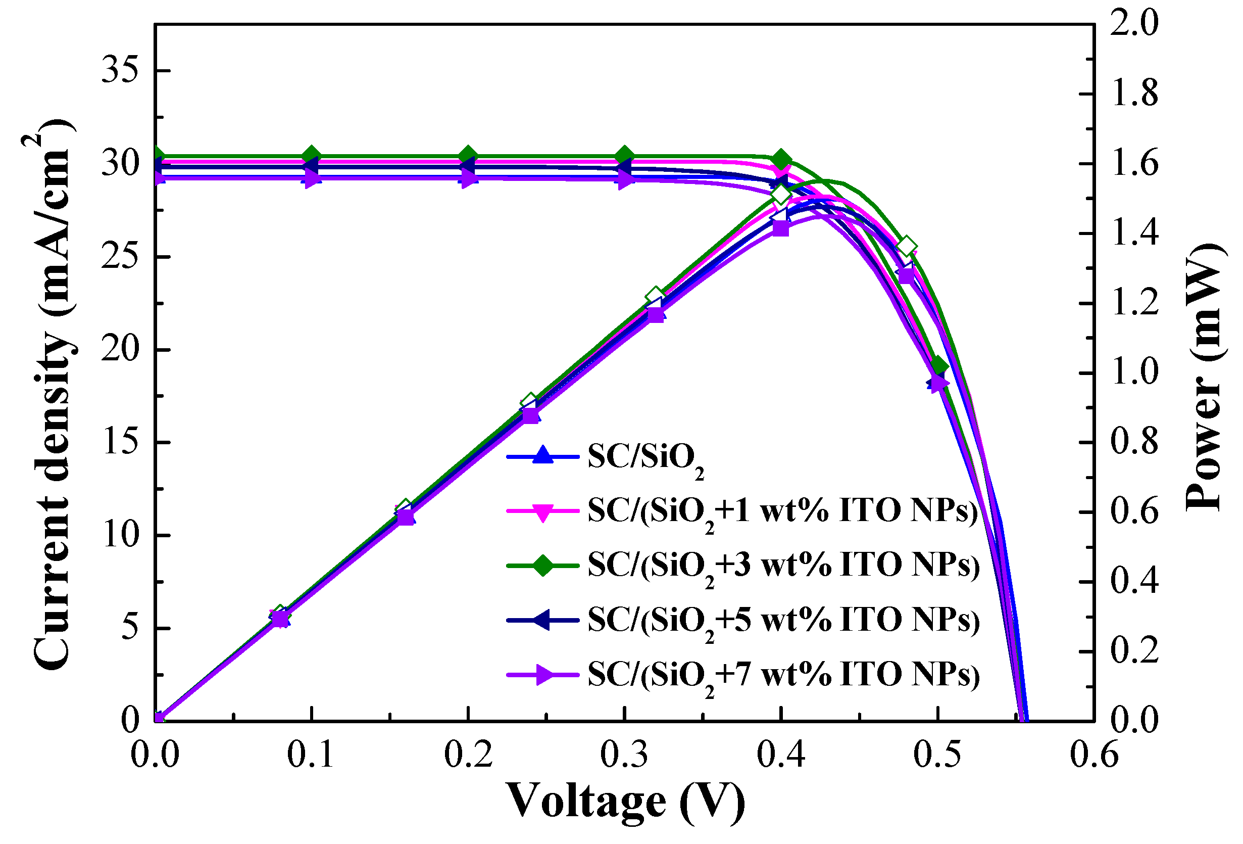
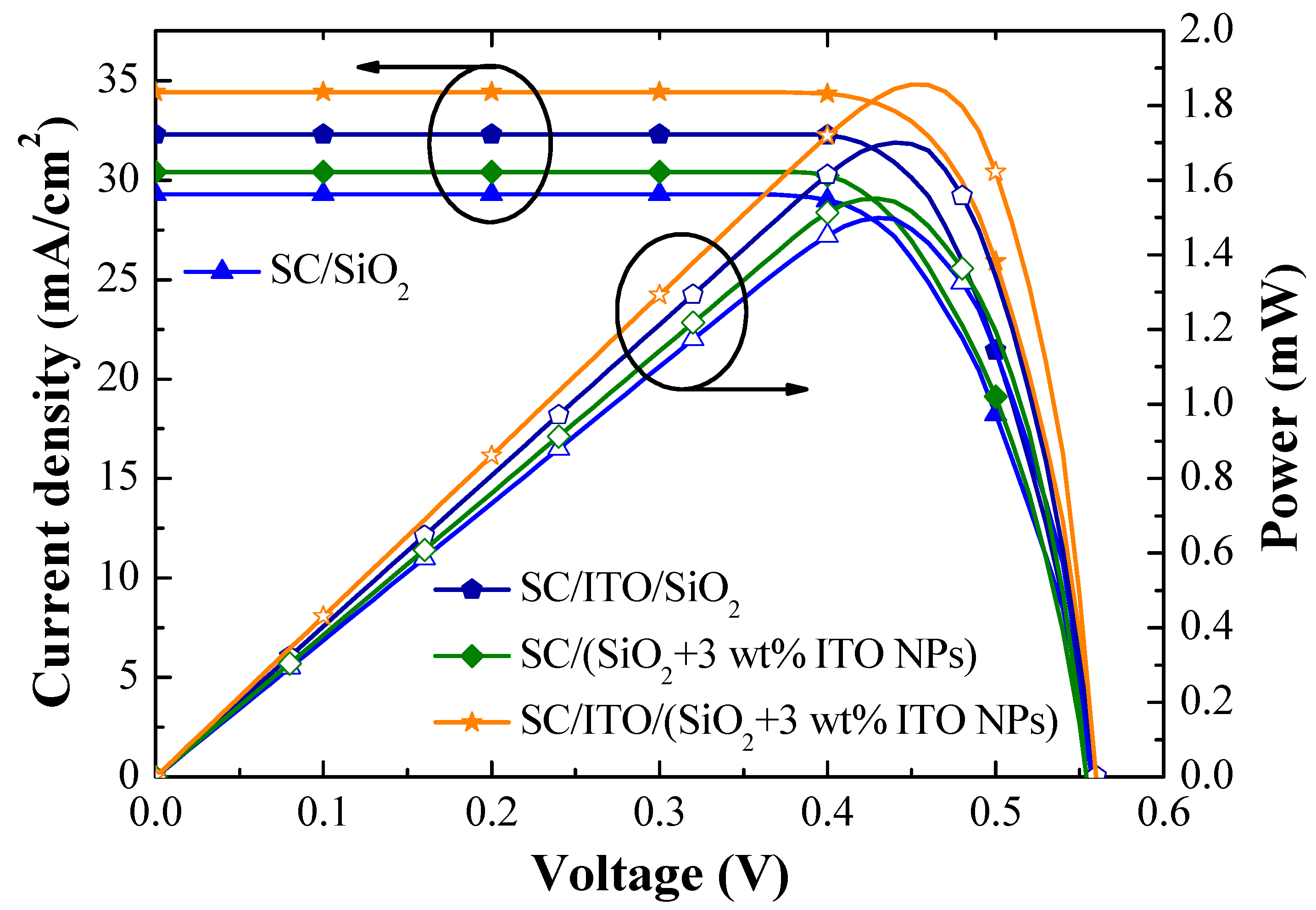
| Solar Cell (SC) Structure | Voc (mV) | Jsc (mA/cm2) | F.F. (%) | η (%) | Pmax (mW) | ΔJsc (%) | Δη (%) |
|---|---|---|---|---|---|---|---|
| Bare SC | 551.01 | 25.65 | 75.51 | 10.67 | 1.33 | - | - |
| SC/ITO | 560.36 | 30.68 | 74.26 | 12.76 | 1.58 | 19.61 | 19.58 |
| SC/SiO2 | 559.01 | 29.30 | 75.08 | 12.30 | 1.49 | 14.23 | 15.27 |
| SC/ITO/SiO2 | 560.40 | 32.30 | 73.98 | 13.47 | 1.70 | 25.92 | 26.24 |
| SC/(SiO2 + 1 wt% ITO-NPs) | 554.10 | 30.01 | 74.77 | 12.43 | 1.51 | 17.00 | 16.49 |
| SC/(SiO2 + 3 wt% ITO-NPs) | 554.01 | 30.41 | 74.71 | 12.58 | 1.55 | 18.55 | 17.90 |
| SC/(SiO2 + 5 wt% ITO-NPs) | 553.91 | 29.71 | 74.33 | 12.23 | 1.46 | 15.82 | 14.62 |
| SC/(SiO2 + 7 wt% ITO-NPs) | 553.80 | 29.06 | 73.98 | 11.90 | 1.45 | 13.29 | 11.52 |
| SC/ITO/(SiO2 +1 wt% ITO-NPs) | 560.59 | 33.49 | 73.81 | 13.86 | 1.80 | 30.56 | 29.89 |
| SC/ITO/(SiO2 +3 wt% ITO-NPs) | 559.91 | 34.43 | 73.76 | 14.22 | 1.86 | 34.23 | 33.27 |
| SC/ITO/(SiO2 +5 wt% ITO-NPs) | 559.13 | 32.84 | 73.51 | 13.50 | 1.73 | 28.03 | 26.52 |
| SC/ITO/(SiO2 +7 wt% ITO-NPs) | 558.86 | 32.38 | 73.22 | 13.25 | 1.69 | 26.23 | 24.17 |
© 2019 by the authors. Licensee MDPI, Basel, Switzerland. This article is an open access article distributed under the terms and conditions of the Creative Commons Attribution (CC BY) license (http://creativecommons.org/licenses/by/4.0/).
Share and Cite
Ho, W.-J.; Chen, G.-Y.; Liu, J.-J. Enhancing Photovoltaic Performance of Plasmonic Silicon Solar Cells with ITO Nanoparticles Dispersed in SiO2 Anti-Reflective Layer. Materials 2019, 12, 1614. https://doi.org/10.3390/ma12101614
Ho W-J, Chen G-Y, Liu J-J. Enhancing Photovoltaic Performance of Plasmonic Silicon Solar Cells with ITO Nanoparticles Dispersed in SiO2 Anti-Reflective Layer. Materials. 2019; 12(10):1614. https://doi.org/10.3390/ma12101614
Chicago/Turabian StyleHo, Wen-Jeng, Guan-Yu Chen, and Jheng-Jie Liu. 2019. "Enhancing Photovoltaic Performance of Plasmonic Silicon Solar Cells with ITO Nanoparticles Dispersed in SiO2 Anti-Reflective Layer" Materials 12, no. 10: 1614. https://doi.org/10.3390/ma12101614
APA StyleHo, W.-J., Chen, G.-Y., & Liu, J.-J. (2019). Enhancing Photovoltaic Performance of Plasmonic Silicon Solar Cells with ITO Nanoparticles Dispersed in SiO2 Anti-Reflective Layer. Materials, 12(10), 1614. https://doi.org/10.3390/ma12101614