Article

Thermochromic and Femtosecond-Laser-Induced Damage Performance of Tungsten-Doped Vanadium Dioxide Films Prepared Using an Alloy Target

1
Key Laboratory of Materials for High Power Laser, Shanghai Institute of Optics and Fine Mechanics, Chinese Academy of Sciences, Shanghai 201800, China
2
University of Chinese Academy of Sciences, Beijing 100049, China
3
Shanghai Institute of Laser Plasma, China Academy of Engineering Physics, Shanghai 201800, China
4
Shenzhen Key Laboratory of Advanced Thin Film and Applications, College of Physics and Energy, Shenzhen University, Shenzhen 518060, China
5
College of Chemistry and Environmental Engineering, Shenzhen University, Shenzhen 518060, China
*
Authors to whom correspondence should be addressed.
Materials 2018, 11(9), 1724; https://doi.org/10.3390/ma11091724
Submission received: 22 August 2018 / Revised: 11 September 2018 / Accepted: 12 September 2018 / Published: 14 September 2018
(This article belongs to the Section Thin Films and Interfaces)

Abstract

:
Thermochromic tungsten-doped VO2 thin films were successfully fabricated using a W-V alloy target. X-ray diffraction analyses showed that the W-doped VO2 film had a preferred orientation of (011), and that the doping did not degrade the film crystallinity compared with that of the pure film. X-ray photoelectron spectroscopy and energy-dispersive spectroscopy showed that the doped 0.81 atom% tungsten replaced vanadium in the lattice of the film. The metal–insulator transition temperature of the W-doped VO2 film was reduced to 35.5 °C, which is close to room temperature. Additionally, the infrared transmittance modulation of the W-doped film at λ = 2500 nm reached 56%, indicating an excellent switching efficiency. The damage behavior of the W-doped VO2 film under a femtosecond-laser irradiation was experimentally investigated. Our results revealed that defect-related damages induced by the femtosecond laser are relevant for W-doped VO2 films. This study provides valuable insights into VO2 films for potential applications in laser protection.

Graphical Abstract

1. Introduction

With the development of the photoelectric detection technology, the effects of high-power lasers on photoelectric detectors have been extensively studied, including high-power-laser-induced damage mechanisms and damage threshold of photoelectric detectors. Protection against high-power lasers using suitable materials has also been studied. Advanced laser protection materials are usually based on conventional linear optics [1]. However, such protection systems not only absorb but also reflect waves of the same wavelength. In other words, the system protects the photoelectric detector from the strong laser; however, it also obstructs the weak waves that carry signals [2]. Therefore, they do not satisfy the requirements for the development of high-power-laser protection systems.
VO2 is a promising material for development of laser protection systems owing to its thermochromic phase-transition characteristics, low threshold laser energy, and fast response [3]. In general, VO2 is a typical thermochromic material which undergoes an extremely abrupt first-order phase transformation from a monoclinic structure to a rutile structure at approximately 68 °C, accompanied by significant changes in its electrical conductivity and infrared (IR) optical transmittance [4,5]. In its low-temperature states (below the transition temperature), VO2 exhibits semiconductor properties, such as a high IR transmission, while in its high-temperature states (above the transition temperature), it exhibits metallic properties, such as a low IR transmission [6]. The light-induced ultrafast phase transition of VO2 occurs in ~10−13 s [7]. These advantages make VO2 promising for various applications including optical switches [8] and solar heat management [9].
When a high-power laser irradiates a photoelectric detector protected by VO2 films, the laser initially interacts with the VO2 films, inducing thermochromic phase transitions. The VO2 films complete the phase transition process before the laser damages the detector; the films then behave as in a metallic state reflecting a large amount of IR energy to reduce the damaging laser energy. This may be an effective approach for high-power-laser protection. The extremely fast response time is crucial for VO2 films used in the field of laser protection. Cavalleri et al. had studied the phase-transition dynamics of VO2 at an extremely small time-scale upon laser excitation using optical pump-probe techniques [10].
The high phase-transition temperature of VO2 of 68 °C limits its applications. Modulation of the transition temperature to room temperature is indispensable for many practical applications, including smart windows. For laser-protection applications, a VO2 film with a high transition temperature could provide a high laser energy input threshold and large response time. The transmitted laser energy may exceed the damage threshold of the detector before the transition of the film; in such a case, the VO2 film has a low protection efficiency. The laser energy that should be absorbed by the VO2 films for phase-transition completion can be obtained by [1]:
E = C   ( T p T a )
where C is the heat capacity of the VO2 thin film, while Tp and Ta are the phase-transition temperature of the VO2 film and environment temperature, respectively. With the decrease in Tp − Ta, the response time of VO2 decreases.
Therefore, the phase-transition temperature of the VO2 film should be reduced to room temperature. In general, doping with high-valence cations, such as Mo6+, Ta5+, Nb5+, and W6+, into the VO2 lattice may be a useful approach to reduce the transition temperature [11,12,13]. Among these cations, W6+ could be the most effective doping cation to regulate the phase-transition temperature of the VO2 film.
Various methods, such as the sol-gel process [14], chemical vapor deposition (CVD) [15], hydrothermal growth [16], and magnetron sputtering [17], have been employed for preparation of tungsten-doped VO2 films with specific thermochromic performances. Among them, the magnetron sputtering technology has advantages for applications in smart windows and laser-protection systems owing to its high packing density [18]. Some studies on tungsten-doped VO2 films prepared by the co-sputtering technique have been reported [5,19]. However, using this method, it could be difficult to precisely control the concentration of the doped tungsten and uniformity of the deposited films. In this study, we used a vanadium–tungsten alloy target (atomic percentage of W: 0.81%) to deposit tungsten-doped VO2 films with a uniform concentration of the doped tungsten. The phase-transition temperature of the W-doped VO2 film can reach a low value of 35.5 °C, which is near room temperature.
The laser-damage behavior of VO2 films, significant for studies of laser-protection systems, has not been extensively investigated. A femtosecond-(fs)-laser-induced breakdown of a film is strongly related with the intrinsic properties of the material. Therefore, in this study, we focused on the fs-laser-induced damage mechanism and laser damage threshold of W-doped VO2 films.

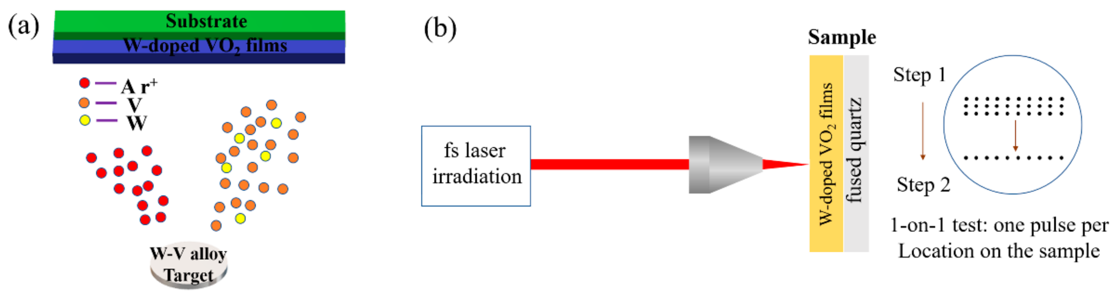
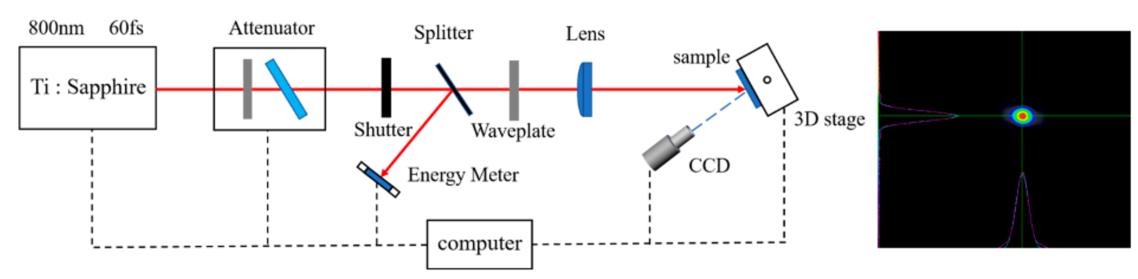
2. Experimental Methods

W-doped VO2 thin films were deposited on fused quartz through DC reactive magnetron sputtering. Regarding the reduction in the phase-transition temperature to room temperature, it has been reported [20,21,22] that the tungsten doping linearly decreases the transition temperature of a VO2 film at an approximate rate of 23 °C/atom%. Based on these studies, a vanadium–tungsten alloy target (atomic percentage of W: 0.81%) was used to prepare the films. The diameter of the target was 60 mm. The distance between the target and glass substrate was approximately 10 cm. Before deposition, the vacuum chamber was pumped to a pressure of approximately 6 × 10⁻⁴ Pa. A pre-sputtering of the vanadium–tungsten alloy target was carried out for approximately 10 min. Ar (99.99%) and O2 (99.99%) were used as the sputtering and reactive gases, respectively. For the deposition of the W-doped films, O2 was mixed with Ar; the flow rates of Ar and O2 were 40 sccm and 1.8 sccm, respectively. The substrate temperature was maintained at 320 °C. The fused quartz substrate was put on the surface of the conductive fixture, which was connected to a DC source with a bias voltage supply of −125 V during the deposition. The sputtering power of the vanadium–tungsten alloy target was 80 W. A schematic of the DC magnetron sputtering process and vanadium–tungsten alloy target is shown in Figure 1a. A schematic of the setup for the fs-laser damage test is shown in Figure 1b. Laser-induced damage threshold (LIDT) tests were performed in the one-on-one mode.
The configuration for the damage tests is illustrated in Figure 2. Laser pulses were generated using a Ti: sapphire regenerative amplifier laser system (Spectra physics), which produced linearly polarized laser pulses with a duration of 60 fs and wavelength of 800 nm at a frequency of 10 Hz. As shown in Figure 2, a λ/2-plate and polarizing beam splitter were used as an attenuator to change the energy of the pulses. A shutter was used to extract a single pulse. Another λ/2-plate in the bottom part was used to change the polarization of the pulses. The samples were mounted on a motorized xz rotation stage and positioned at the focal plane of the lens; the e−2-intensity diameter of the laser spot at the focus was measured to be approximately 320 μm. The pulse energy was measured in the reference path, split using a beam splitter. In-situ imaging of the front surface of the sample combined with ex-situ optical microscopy observations was carried out to monitor the occurrence of damage.
X-ray diffraction (XRD) (Ultima IV, Rigaku, Tokyo, Japan) analyses were carried out to evaluate the crystalline structures of the W-doped films. The chemical composition of the W-doped VO2 film was evaluated using a X-ray photoelectron spectroscope (XPS) (Thermo K-Alpha XPS, Thermo Scientific, Waltham, MA, USA). A four-point probe system was used to characterize the temperature-dependent sheet resistances of the W-doped VO2 films. During the measurement, the film temperature was controlled in the range of room temperature to 70 °C. The normal-incidence spectral transmittances of the W-doped films at temperatures below and above the transition temperatures were measured using a ultraviolet-visible-near-IR (UV-VIS-NIR) spectrophotometer (Lambda 950, PerkinElmer, Waltham, MA, USA). The surface morphologies and roughness values of the W-doped samples were measured using a field-emission scanning electron microscope (FE-SEM) (Supra 55, Zeiss, Oberkochen, Germany) and atomic force microscope (Dimension 3100, Veeco, Bruker, Karlsruhe, Germany), respectively. The surface morphologies of damaged sites were observed in detail using an optical microscope (Leica, Solms, Germany) and FE-SEM (Auriga S40, Zeiss, Munich, Germany).

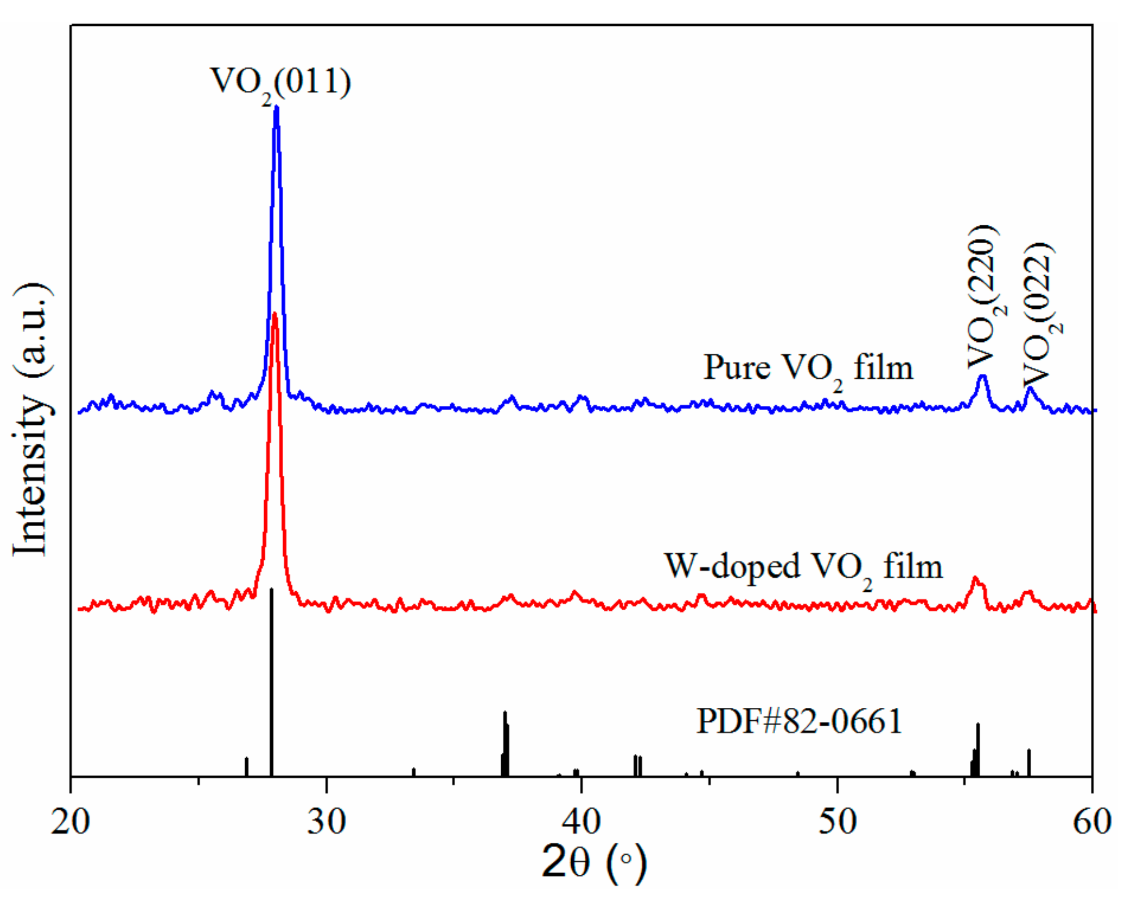
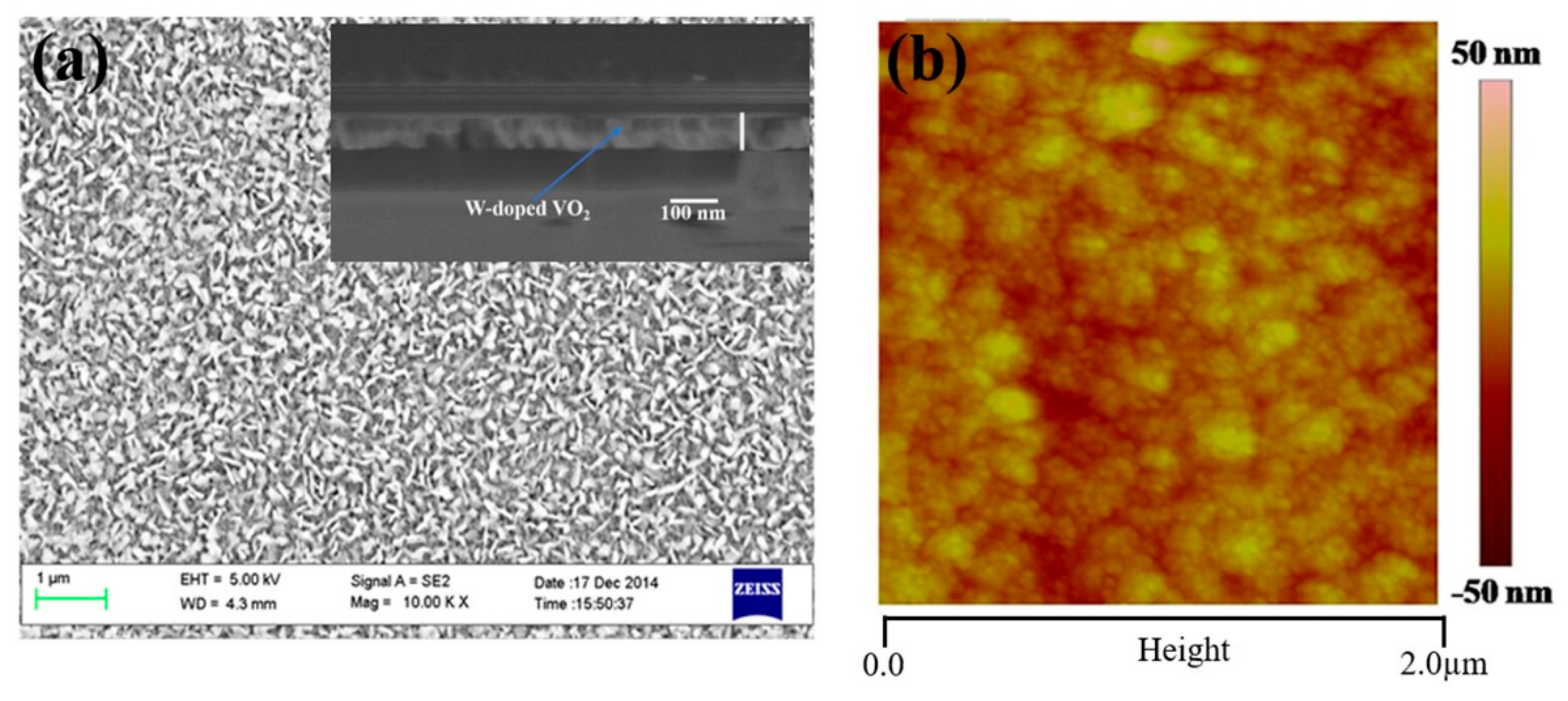
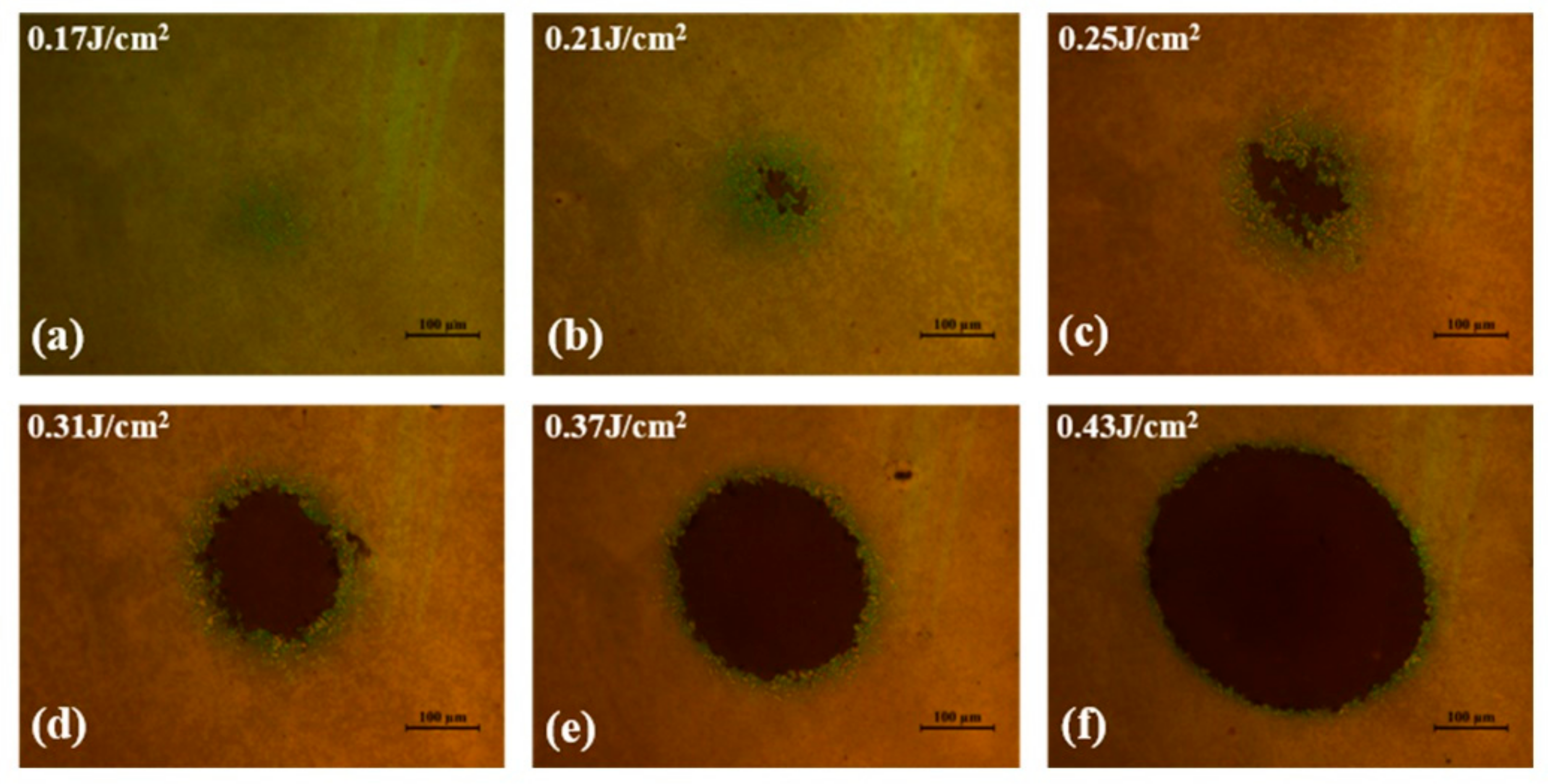
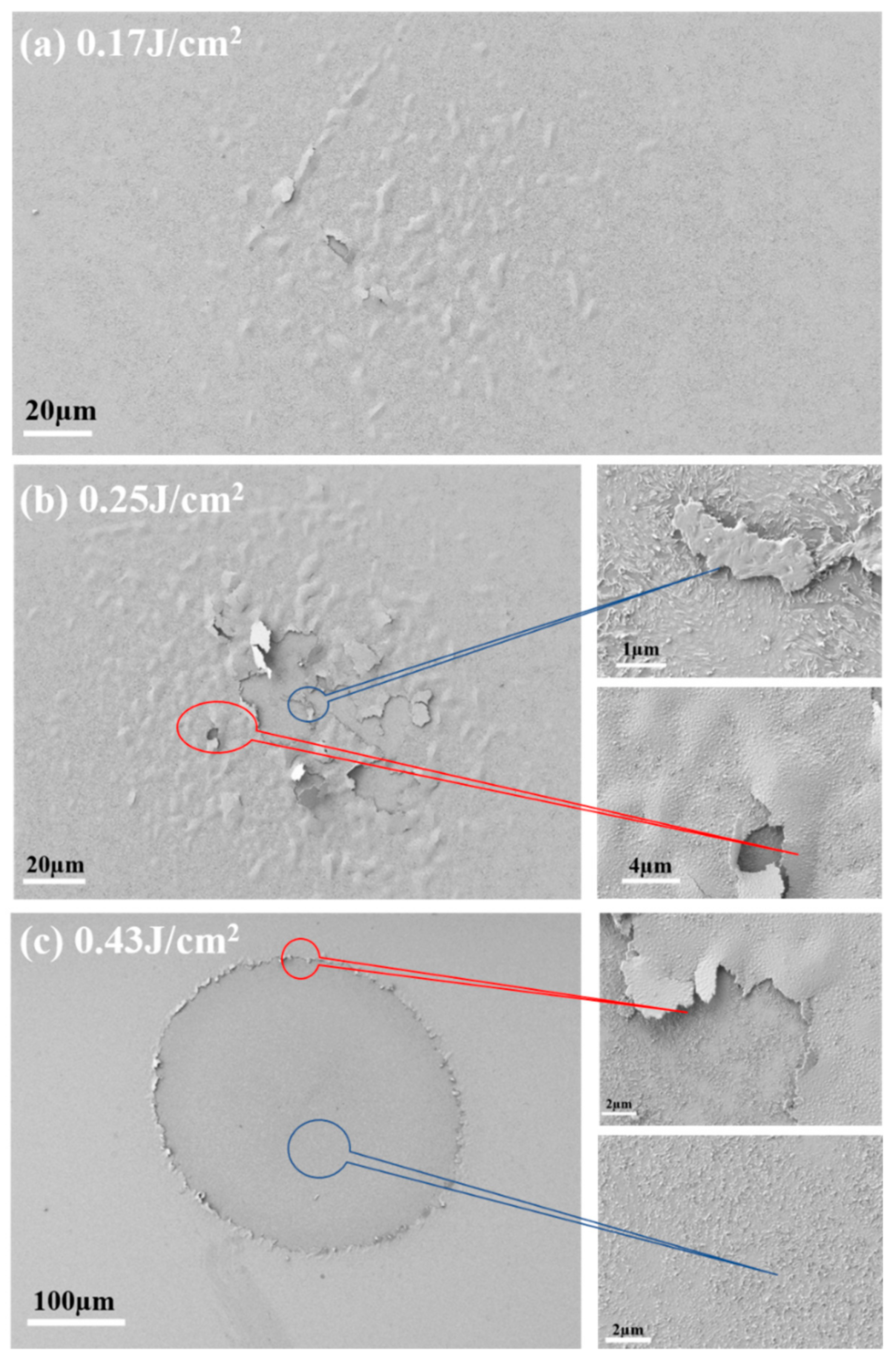
3. Results and Discussion

Figure 3 shows XRD patterns of the W-doped and pure VO2 thin films, and standard pattern of the VO2 phase (PDF#82-0661). The diffraction peaks of the W-doped and pure films are similar and correspond to the characteristic pattern of the VO2 phase. It is worth noting that no other impurity peaks can be observed from the XRD patterns, which indicates the formation of single-phase W-doped VO2 films. Additionally, the W-doped sample exhibited a preferential growth in the (011) lattice orientation, which is consistent with other reports [23,24]. Moreover, the (011) peak of the W-doped VO2 film slightly shifted to a lower 2θ value compared with that of the pure VO2 film, revealing a small distortion of the lattice as the atomic radii of tungsten and vanadium are different (tungsten introduced in the VO2 crystal lattice replaces vanadium).
For a more detailed analysis, the grain size of the film was estimated using Scherrer’s formula, D = 0.9λ/cosθ·Δ, where λ is the X-ray wavelength, D is the crystallite size, Δ2θ is the peak full-width at half-maximum (FWHM) (corrected for instrumental broadening), and θ is the angle [25]. The most intense peak of (011) was used to calculate the grain sizes, yielding values of 16.2 and 15.5 nm for the W-doped and pure VO2 films, respectively. Compared with the pure VO2 film, the W-doped VO2 film had an excellent crystallinity. These results suggest that the tungsten doping through the proposed vanadium-tungsten alloy target method did not reduce the crystallinity of the W-doped VO2 film.
Figure 4a shows the surface morphology of the W-doped VO2 film. Small rice-like grains were uniformly spread over the film surface, which confirms the uniformity and crystallinity of the W-doped VO2 film. The cross-sectional SEM image of the W-doped VO2 film in the inset shows the 90-nm-thick W-doped VO2. We calculated the transmittance of the film using reported optical constants [26] and thickness of 90 nm, which is consistent with the measured transmittance. A topographic AFM image of the W-doped VO2 film is presented in Figure 4b, showing that the surface is continuous and homogeneous. The root-mean-square (RMS) roughness was approximately 6.10 nm, which demonstrates the good surface quality of the W-doped VO2 film.
The chemical state and composition of the tungsten-doped VO2 film were investigated by a typical XPS spectrum analysis, as shown in Figure 5. The C 1s peak (284.6 eV) was used for calibration in the XPS spectrum measurements. The obtained wide-range XPS spectrum, shown in Figure 5a, indicates that several elements (V, O, W, Si, and C) were present in the W-doped sample; the presence of carbon could be attributed to surface contamination. Figure 5b presents high-resolution scanning results for the V 2p3/2 peak, which is the most sensitive peak to the phase changes of VO2 [27]. Vanadium was present in three main components, with peaks at 515.0 eV, 516.0 eV, and 516.7 eV corresponding to V3+, V4+, and V5+, respectively [28,29]. The relative concentrations of V3+, V4+, and V5+ in the W-doped VO2 film were calculated to be 21.71%, 62.36%, and 15.93%, respectively. This reveals that the W-doped VO2 film is good, achieved through the precise control of the oxygen flow rate in the experiment. Additionally, the use of the vanadium–tungsten alloy target to deposit the tungsten-doped VO2 film ensured the uniformity of the film and concentration of the doped tungsten, which are beneficial to the formation of the W-doped VO2 film. A weak peak of W 4f7/2 can be observed in Figure 5c, demonstrating the successful doping of the film with tungsten ions. According to the report of Huang et al. [27], the peak of W 4f7/2 at 35.4 eV corresponds to W6+.
The results of the energy-dispersive spectroscopy (EDS) analysis of the W-doped sample are shown in Figure 6. Peaks attributed to vanadium and tungsten elements can be observed in the EDS pattern, indicating that the VO2 film was successfully doped with tungsten. The concentrations of vanadium and tungsten elements were determined to be 99.19 atom% and 0.81 atom%, respectively, in good agreement with the content ratio of the used vanadium–tungsten alloy target. Therefore, the W-doped VO2 film had a composition of V0.9919W0.0081O2, consistent with the XPS data.
The sheet resistances as a function of the temperature for the W-doped and undoped VO2 films are shown in Figure 7a. Both samples exhibited the expected thermal hysteresis; however, their sheet resistances were different. The sheet resistance of the W-doped VO2 film was lower than that of the pure VO2 film. The XPS results in Figure 5 show that the W-doped VO2 film contains V2O3, V2O5, and VO2. However, the pure VO2 film mainly consists of VO2 and V2O5, reported in our previous study [30]. The existence of V2O3 in the film decreases its resistance. For the W-doped VO2 film, the addition of tungsten may break V4+–V4+ bonds, forming V3+–W6+ and V3+–V4+ pairs for charge compensation [31]. In this case, the W-doping provides extra electrons to the surrounding V atoms and decreases the resistance in the insulating phase of the W-doped VO2 film. Figure 7b shows standard Gaussian-fitted derivative logarithmic plots of the films. The transition temperatures of the W-doped and pure VO2 films were 35.5 °C and 54.5 °C, respectively. These results show that the tungsten doping can effectively reduce the transition temperature of VO2, consistent with the results of Jin et al. [20], Li et al. [21], and Liang et al. [22], where the tungsten doping linearly decreased the transition temperature of the VO2 film at an approximate rate of 23 °C/atom%. The W-doping concentration in this study was approximately 0.81 atom%, determined from the EDS result in Figure 6. Using the above formula, the calculated Tc for the W-doped VO2 film is about 36 °C ((54.5(Tc of pure VO2) − 0.81 × 23) °C ≈ 36 °C), which is close to our experimentally obtained value of 35.5 °C. This demonstrates that the doping concentration of tungsten ions can be precisely controlled using the vanadium–tungsten alloy target.
A W6+ ion introduced into the VO2 lattice breaks one homopolar V4+–V4+ bond. For charge compensation, two d-shell electrons from the tungsten ion transfer into the neighboring vanadium ions to form V3+–W6+ along the a-axis of the monoclinic VO2 cell. With the increase in the fraction of W6+ in the lattice, the loss of homopolar V4+–V4+ bonds progressively increases, leading to destabilization of the semiconductor phase [32,33], which decreases the transition temperature of VO2.
The transmittance of the W-doped VO2 film was measured in the range of 250 nm to 2500 nm at 20 °C and 70 °C, as shown in Figure 8a. The W-doped sample exhibited a significantly higher IR transmittance in the semiconductive state (20 °C) than that in the metallic state (70 °C), indicating that the VO2 film had a high IR-switching performance. The IR transmittance at λ = 2500 nm was 75% before the phase transition, which decreased to 19% after the phase transition. The IR modulation value of the W-doped sample at λ = 2500 nm reached 56%, better than our previous result for a pure VO2 film [34]. In the visible range (390–780 nm), the peak transmittance of the W-doped VO2 sample was approximately 50%, which indicates a good luminous transmittance. Moreover, the IR modulation and luminous transmittance of the W-doped VO2 film are better than those of reported W-doped VO2 films prepared by aerosol-assisted chemical vapor deposition [35] and atmospheric-pressure chemical vapor deposition [36]. Figure 8b shows the optical transmittance of the pure VO2 film with a thickness (90 nm) equal to that of the W-doped VO2 film. The luminous and IR optical transmittances of the W-doped VO2 film are slightly lower than those of the pure VO2 film.
Figure 9 shows the statistical results of the laser damage test of the W-doped VO2 film. The one-on-one LIDT of the W-doped VO2 film was 0.14 ± 0.01 J/cm2, estimated by the damaged-area-extrapolation method, using the relationship between the logarithm of the laser fluence and damaged area [37,38]. The optical morphologies of portions of the W-doped VO2 film damaged by the fs-laser are shown in Figure 10. The damage mechanism depends on the fluence level. At a fluence level just above the damage threshold, the damaged site is characterized by surface coloring, which indicates an enhanced roughness. The size of the colored region increases with the incident fluence; ablation in the center of the damaged site occurs when the fluence reaches 0.25 J/cm2. At higher fluence levels, the ablated region develops significantly faster than the colored region and eventually occupies most of the damaged site.
The high-resolution SEM images in Figure 11 reveal that the colored region contained abundant isolated microbuckling nodules; certain microbuckling nodules were broken owing to higher localized energies. The isolated microbuckling nodules can lead to fluctuations of the coating surface and roughness enhancement. With the increase in the fluence level, more microbuckling nodules were broken. The ablation in the center of the damaged site was invisible until the broken microbuckling nodules joined. Therefore, there are two damage thresholds: buckling and breaking thresholds. The former is related to the surface coloring phenomenon observed in the optical morphology of the film, while the latter is related to the ablation phenomenon. A transitive threshold (~0.21 J/cm2) was defined to determine the fluence required to transition from isolated microbuckling nodules to integral ablation. The joining process of the isolated microbuckling nodules can be observed from the edge of the damaged site in Figure 11c. Similar phenomena have been reported in our previous study for dielectric coatings damaged using an 800-fs laser [39]. Large amounts of defects or impurities may exist at the surface of the W-doped VO2 film due to the metal doping. At a fluence level just above the damage threshold, coating defects can induce local light field enhancements at the nanoscale. Additionally, the absorption coefficient of defects is high [37]. The above two factors may contribute to the increase in density of electrons surrounding defects during the pulse irradiation. When the free-electron density reached a critical plasma density, the laser energy was strongly absorbed by the forming plasma, leading to small damage spots [40]. This phenomenon can be observed in Figure 10a. With the increase in the pulse energy, the outline of the damaged area becomes clearer and large-scale ablation can be observed in Figure 10b–f. In this case, the damage in the fs-regime is intrinsic and the coating spalling becomes more significant than the impact of defects. The role of defects in laser-induced modifications of dielectric materials has also been studied by Laurence et al. [41] and Gallais et al. [42]. According to the results of this study, the defect-related damage induced by fs-lasers is important for semiconductive materials. It is necessary to study the damaging process in detail, which can be a subject of a following study.

4. Conclusions

Thermochromic tungsten-doped VO2 thin films were successfully fabricated using a W–V alloy target. The damage behavior of the W-doped VO2 films under a fs-laser irradiation was investigated experimentally and theoretically. The results showed that 0.81 atom% W6+ replaced vanadium in the lattice of the W-doped sample. The metal-insulator transition temperature of the W-doped VO2 film was approximately 35.5 °C, which is near room temperature. The W-doped VO2 film exhibited an excellent thermochromic performance. Laser-induced damage tests were performed with 800-nm 60-fs pulses; the LIDT for the W-doped VO2 film was approximately 0.14 J/cm2. The defect-related damage induced by fs-lasers is relevant for W-doped VO2 films. This study provided valuable insights regarding VO2 films used for laser protection.

Author Contributions

M.Z., H.Q. and D.Z. designed the experiments; M.Z. and C.S. grew and characterized the W-doped VO2 film samples; C.S., C.L. and H.W. carried out the laser damage testing of W-doped VO2 films; W.L. performed the XPS measurement of W-doped VO2 films and analyzed the related data; M.Z., H.Q. and D.Z. wrote and revised the paper.

Funding

This research received no external funding.

Acknowledgments

We acknowledge the support from the Shenzhen Science and Technology Project (JCYJ20150529164656098, ZDSY20170228105421966); Research and Development Fund of Guangdong/Shenzhen (2016B090930011, JCYJ20160226192609015).

Conflicts of Interest

The authors declare no conflict of interest.

References

  1. Lu, Y.; Feng, Y.S.; Ling, Y.S.; Qiao, Y. The mechanism of laser disturbing infrared detector and its intelligent protection. Proc. SPIE 2013, 8904, 89040T. [Google Scholar]
  2. Huang, Z.L.; Chen, S.H.; Lv, C.H.; Huang, Y.; Lai, J.J. Infrared characteristics of VO2 thin films for smart window and laser protection. Appl. Phys. Lett. 2012, 101, 191905. [Google Scholar] [CrossRef]
  3. Beebe, M.R.; Klopf, J.M.; Wang, Y.; Kittiwatanakul, S.; Lu, J.; Wolf, S.A.; Lukaszew, R.A. Time-resolved lightinduced insulator-metal transition in niobium dioxide and vanadium dioxide thin films. Opt. Mater. Express 2017, 7, 213–223. [Google Scholar] [CrossRef]
  4. Song, S.C.; Ma, X.L.; Pu, M.B.; Li, X.; Guo, Y.H.; Gao, P.; Luo, X.G. Tailoring active color rendering and multiband photodetection in a vanadium-dioxide-based metamaterial absorber. Photonics Res. 2018, 6, 492–497. [Google Scholar] [CrossRef]
  5. Dietrich, M.K.; Kuhl, F.; Polity, A.; Klar, P.J. Optimizing thermochromic VO2 by co-doping with W and Sr for smart window applications. Appl. Phys. Lett. 2017, 110, 141907. [Google Scholar] [CrossRef]
  6. Currie, M.; Mastro, M.A.; Wheeler, V.D. Characterizing the tunable refractive index of vanadium dioxide. Opt. Mater. Express 2017, 7, 1697–1707. [Google Scholar] [CrossRef]
  7. Lysenko, S.; Rúa, A.; Vikhnin, V.; Fernández, F.; Liu, H. Insulator-to-metal phase transition and recovery processes in VO2 thin films after femtosecond laser excitation. Phys. Rev. B 2007, 76, 035104. [Google Scholar] [CrossRef]
  8. Chen, L.; Ye, H.; Liu, Y.M.; Wu, D.; Ma, R.; Yu, Z.Y. Numerical investigations of an optical switch based on a silicon stripe waveguide embedded with vanadium dioxide layers. Photonics Res. 2017, 5, 335–339. [Google Scholar] [CrossRef]
  9. Madida, I.G.; Simo, A.; Sone, B.; Maity, A.; Kana, J.B.; Gibaud, A.; Merad, G.; Thema, F.T.; Maaza, M. Submicronic VO2-PVP composites coatings for smart windows applications and solar heat management. Sol. Energy 2014, 107, 758–769. [Google Scholar] [CrossRef]
  10. Cavalleri, A.; Dekorsy, T.; Chong, H.H.W.; Kieffer, J.C.; Schoenlein, R.W. Evidence for a structurally driven insulator-to-metal transition in VO2: A view from the ultrafast timescale. Phys. Rev. B 2004, 70, 161102. [Google Scholar] [CrossRef]
  11. Chang, S.J.; Park, J.B.; Lee, G.; Kim, H.J.; Lee, J.B.; Bae, T.S.; Han, Y.K.; Park, T.J.; Huh, Y.S.; Hong, W.K. In situ probing of doping-and stress-mediated phase transitions in a single-crystalline VO2 nanobeam by spatially resolved Raman spectroscopy. Nanoscale 2014, 6, 8068–8074. [Google Scholar] [CrossRef] [PubMed]
  12. Zhang, Y.; Li, W.; Fan, M.; Zhang, F.; Zhang, J.; Liu, X.; Zhang, H.; Huang, C.; Li, H. Preparation of Wand Mo doped VO2(M) by ethanol reduction of peroxovanadium complexes and their phase transition and optical switching properties. J. Alloys Compd. 2012, 544, 30–36. [Google Scholar] [CrossRef]
  13. Ji, C.H.; Wu, Z.M.; Feng, H.Q.; Wang, J.; Huang, Z.H.; Zhou, H.X.; Yao, W.; Gou, J.; Jiang, Y.D. Optimization of metal-to-insulator phase transition properties in polycrystalline VO2 films for terahertz modulation applications by doping. J. Mater. Chem. C 2018, 6, 1722–1730. [Google Scholar] [CrossRef]
  14. Ji, H.N.; Liu, D.Q.; Cheng, H.F.; Zhang, C.Y. Inkjet printing of vanadium dioxide nanoparticles for smart windows. J. Mater. Chem. C 2018, 6, 2424–2429. [Google Scholar] [CrossRef]
  15. Shi, R.; Wang, J.W.; Cai, X.B.; Zhang, L.F.; Chen, P.C.; Liu, S.Y.; Zhang, L.; Ouyang, W.K.; Wang, N.; Cheng, C. Axial Modulation of Metal−Insulator Phase Transition of VO2 Nanowires by Graded Doping Engineering for Optically Readable Thermometers. J. Phys. Chem. C 2017, 121, 24877–24885. [Google Scholar] [CrossRef]
  16. Wu, S.W.; Tian, S.Q.; Liu, B.S.; Tao, H.Z.; Zhao, X.J.; Palgrave, R.G.; Sankar, G.; Parkin, I.P. Facile synthesis of mesoporous VO2 nanocrystals by a cotton-template method and their enhanced thermochromic properties. Sol. Energy Mater. Sol. Cells 2018, 176, 427–434. [Google Scholar] [CrossRef]
  17. Vlček, J.; Kolenatý, D.; Houška, J.; Kozák, T.; Čerstvý, R. Controlled reactive HiPIMS-effective technique for low-temperature (300 °C) synthesis of VO2 films with semiconductor-to-metal transition. J. Phys. D Appl. Phys. 2017, 50, 38LT01. [Google Scholar] [CrossRef]
  18. Zhang, D.P.; Zhu, M.D.; Liu, Y.; Yang, K.; Liang, G.X.; Zheng, Z.H.; Cai, X.M.; Fan, P. High performance VO2 thin films growth by DC magnetron sputtering at low temperature for smart energy efficient window application. J. Alloys Compd. 2016, 659, 198–202. [Google Scholar] [CrossRef]
  19. Paone, A.; Sanjines, R.; Jeanneret, P.; Whitlow, H.J.; Guibert, E.; Guibert, G.; Bussy, F.; Scartezzini, J.L.; Schüler, A. Influence of doping in thermochromic V1−xWxO2 and V1−xAlxO2 thin films: Twice improved doping efficiency in V1−xWxO2. J. Alloys Compd. 2015, 621, 206–211. [Google Scholar] [CrossRef]
  20. Jin, P.; Tanemura, S. Relationship between Transition Temperature and x in V1−xWxO2 Films Deposited by Dual-Target Magnetron. Jpn. J. Appl. Phys. 1995, 34, 2459–2460. [Google Scholar] [CrossRef]
  21. Li, W.J.; Ji, S.D.; Li, Y.M.; Huang, A.; Luo, H.J.; Jin, P. Synthesis of VO2 nanoparticles by a hydrothermal-assisted homogeneous precipitation approach for thermochromic applications. RSC Adv. 2014, 4, 13026–13033. [Google Scholar] [CrossRef]
  22. Liang, S.; Shi, Q.W.; Zhu, H.F.; Peng, B.; Huang, W.X. One-Step Hydrothermal Synthesis of W-Doped VO2(M) Nanorods with a Tunable Phase-Transition Temperature for Infrared Smart Windows. ACS Omega 2016, 1, 1139–1148. [Google Scholar] [CrossRef]
  23. Mao, Z.P.; Wang, W.; Liu, Y.; Zhang, L.P.; Xu, H.; Zhong, Y. Infrared stealth property based on semiconductor (M)-to-metallic (R) phase transition characteristics of W-doped VO2 thin films coated on cotton fabrics. Thin Solid Films 2014, 558, 208–214. [Google Scholar] [CrossRef]
  24. Zhu, M.D.; Qi, H.J.; Wang, B.; Wang, H.; Zhang, D.P.; Lv, W.Z. Enhanced visible transmittance and reduced transition temperature for VO2 thin films modulated by index-tunable SiO2 anti-reflection coatings. RSC Adv. 2018, 8, 28953–28959. [Google Scholar] [CrossRef]
  25. Brassard, D.; Fourmanux, S.; Jean-Jacques, M.; Kieffer, J.C.; Khakania, M.A. Grain size effect on the semiconductor-metal phase transition characteristics of magnetron-sputtered thin films. Appl. Phys. Lett. 2005, 87, 051910. [Google Scholar] [CrossRef]
  26. Houska, J.; Kolenaty, D.; Vlcek, J.; Cerstvy, R. Properties of thermochromic VO2 films prepared by HiPIMS onto unbiased amorphous glass substrates at a low temperature of 300 °C. Thin Solid Films 2018, 660, 463–470. [Google Scholar] [CrossRef]
  27. Huang, Z.L.; Chen, C.H.; Lv, C.H.; Chen, S.H. Tungsten-doped vanadium dioxide thin films on borosilicate glass for smart window application. J. Alloys Compd. 2013, 564, 158–161. [Google Scholar] [CrossRef]
  28. Lin, T.G.; Wang, L.P.; Wang, X.F.; Zhang, Y.F.; Yu, Y.H. Influence of bias voltage on microstructure and phase transition properties of VO2 thin film synthesized by HiPIMS. Surf. Coat. Technol. 2016, 305, 110–115. [Google Scholar] [CrossRef]
  29. Silversmit, G.; Depla, D.; Poelman, H.; Marin, G.B.; Gryse, R.D. Determination of the V2p XPS binding energies for different vanadium oxidation states (V5+ to V0+). J. Electron Spectrosc. 2004, 135, 167–175. [Google Scholar] [CrossRef]
  30. Zhu, M.D.; Qi, H.J.; Li, C.; Wang, B.; Wang, H.; Guan, T.R.; Zhang, D.P. VO2 thin films with low phase transition temperature grown on ZnO/glass by applying substrate DC bias at low temperature of 250 °C. Appl. Surf. Sci. 2018, 453, 23–30. [Google Scholar] [CrossRef]
  31. Wu, Y.F.; Fan, L.L.; Huang, W.F.; Chen, S.M.; Chen, S.; Chen, F.H.; Zou, C.W.; Wu, Z.Y. Depressed transition temperature of WxV1-xO2: Mechanistic insights from the X-ray absorption fine structure (XAFS) spectroscopy. Phys. Chem. Chem. Phys. 2014, 16, 17705–17714. [Google Scholar] [CrossRef] [PubMed]
  32. Pan, M.; Zhong, H.M.; Wang, S.W.; Liu, J.; Li, Z.F.; Chen, X.S.; Lu, W. Properties of VO2 thin film prepared with precursor VO (acac) (2). J. Cryst. Growth 2004, 265, 121–126. [Google Scholar] [CrossRef]
  33. Ye, J.W.; Zhou, L.; Liu, F.J.; Qi, J.; Gong, W.T.; Lin, Y.; Ning, G.L. Properties of thermochromic tungsten-doped vanadium dioxide by thermal reduction and annealing. J. Alloys Compd. 2010, 504, 503–507. [Google Scholar] [CrossRef]
  34. Zhu, M.D.; Qi, H.J.; Wang, B.; Wang, H.; Guan, T.R.; Zhang, D.P. Thermochromism of vanadium dioxide films controlled by the thickness of ZnO buffer layer under low substrate temperature. J. Alloys Compd. 2018, 740, 844–851. [Google Scholar] [CrossRef]
  35. Piccirillo, C.; Binions, R.; Parkin, I.P. Synthesis and characterisation of W-doped VO2 by Aerosol Assisted Chemical Vapour Deposition. Thin Solid Films 2008, 516, 1992–1997. [Google Scholar] [CrossRef]
  36. Manning, T.D.; Parkin, I.P.; Pemble, M.E.; Sheel, D.; Dimitra, V. Intelligent Window Coatings: Atmospheric Pressure Chemical Vapor Deposition of Tungsten-Doped Vanadium Dioxide. Chem. Mater. 2004, 16, 744–749. [Google Scholar] [CrossRef]
  37. Natoli, J.Y.; Gallais, L.; Akhouayri, H.; Amra, C. Laser-induced damage of materials in bulk, thin-film, and liquid forms. Appl. Opt. 2002, 41, 3156–3166. [Google Scholar] [CrossRef] [PubMed]
  38. Liu, J.M. Simple technique for measurements of pulsed Gaussian-beam spot sizes. Opt. Lett. 1982, 7, 196–198. [Google Scholar] [CrossRef] [PubMed]
  39. Wang, H.; Qi, H.J.; Zhao, J.L.; Wang, B.; Shao, J.D. Transition from isolated submicrometer pits to integral ablation of HfO2 and SiO2 films under subpicosecond irradiation. Opt. Commun. 2017, 387, 214–222. [Google Scholar] [CrossRef]
  40. Yuan, L. Comparison of femtosecond and nanosecond laser-induced damage in HfO2 single-layer film and HfO2-SiO2 high reflector. J. Opt. Soc. Am. B 2007, 24, 538–543. [Google Scholar] [CrossRef]
  41. Laurence, T.A.; Negres, R.A.; Ly, S.; Shen, N.; Carr, C.W.; Alessi, D.A.; Rigatti, A.; Bude, J.D. Role of defects in laser-induced modifications of silica coatings and fused silica using picosecond pulses at 1053 nm: II. Scaling laws and the density of precursors. Opt. Express 2017, 25, 15381–15401. [Google Scholar] [CrossRef] [PubMed]
  42. Gallais, L.; Capoulade, J.; Natoli, J.Y.; Commandré, M. Investigation of nanodefect properties in optical coatings by coupling measured and simulated laser damage statistics. J. Appl. Phys. 2008, 104, 053120. [Google Scholar] [CrossRef]
Figure 1. (a) Schematic of the DC magnetron sputtering system and vanadium-tungsten alloy target. (b) Schematic of the setup for the fs-laser damage tests.
Materials 11 01724 g001
Figure 2. (Left) Experimental setup for laser damage tests at 60 fs and 800 nm. (Right) Image of the laser beam intensity distribution at the sample location.
Materials 11 01724 g002
Figure 3. XRD patterns of the pure and W-doped VO2 films.
Materials 11 01724 g003
Figure 4. SEM and AFM images of the W-doped VO2 film.
Materials 11 01724 g004
Figure 5. Typical XPS spectra of the W-doped VO2 film: (a) survey spectrum and high-resolution scans of (b) V 2p3/2 and (c) W 4f7/2.
Materials 11 01724 g005
Figure 6. EDS pattern of the W-doped VO2 film.
Materials 11 01724 g006
Figure 7. (a) Resistance–temperature hysteresis loops and (b) phase-transition temperatures of the pure and W-doped VO2 films.
Materials 11 01724 g007
Figure 8. Transmission spectra of the (a) W-doped and (b) pure VO2 films before and after their phase transitions.
Materials 11 01724 g008
Figure 9. Damage area as a function of the fluence for the W-doped VO2 film; the error bars were obtained using the practically measured energy fluence.
Materials 11 01724 g009
Figure 10. Optical morphologies of the W-doped VO2 film under different laser fluence levels.
Materials 11 01724 g010
Figure 11. SEM morphologies of the W-doped VO2 film under different fluence levels of (a) 0.17, (b) 0.25, and (c) 0.43 J/cm2. The right-hand subfigures in (b,c) are partial enlarged images.
Materials 11 01724 g011

