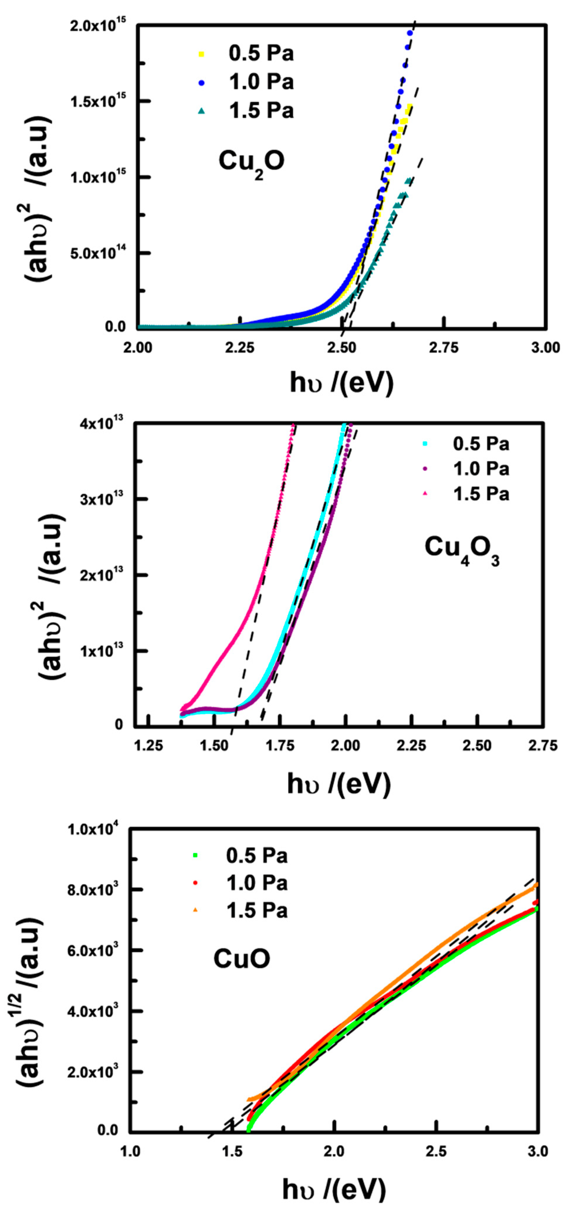
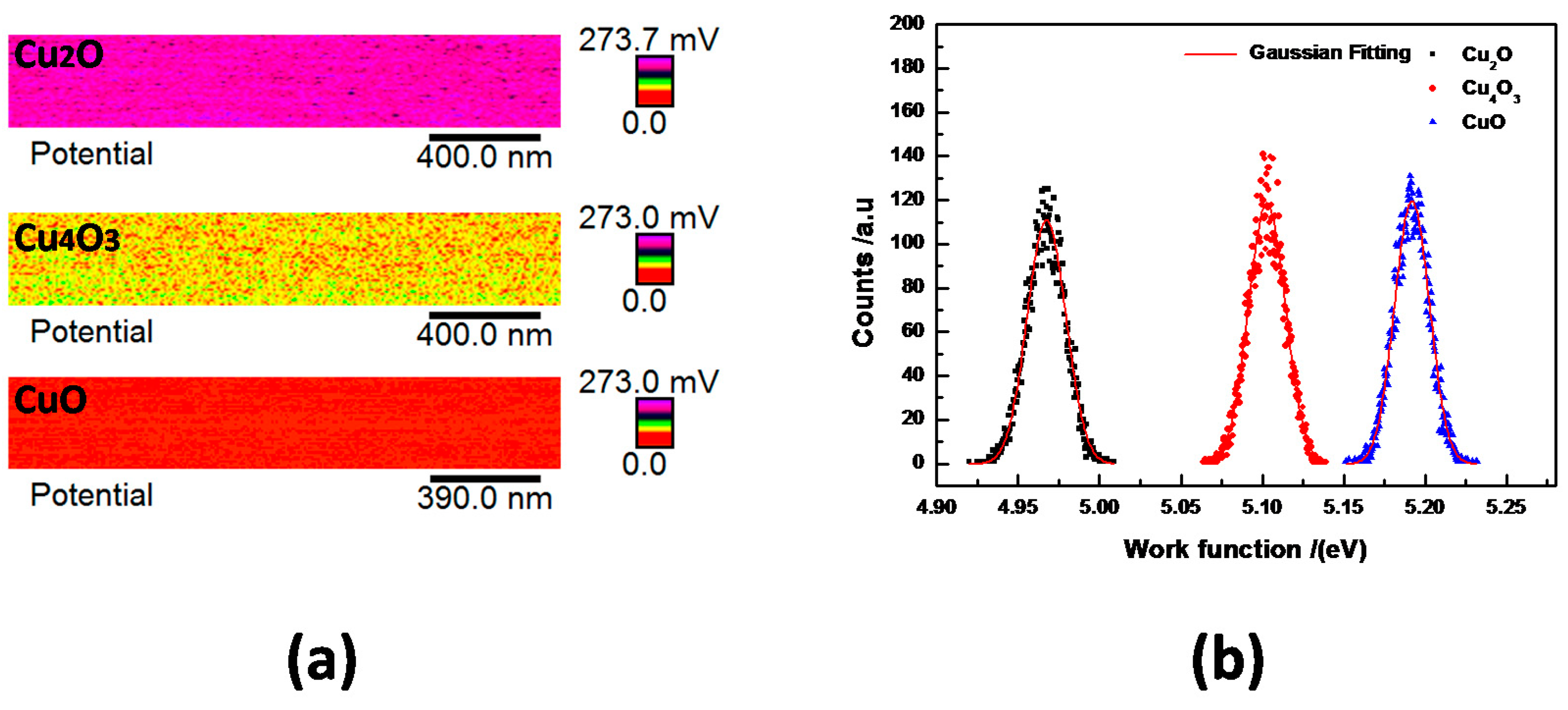
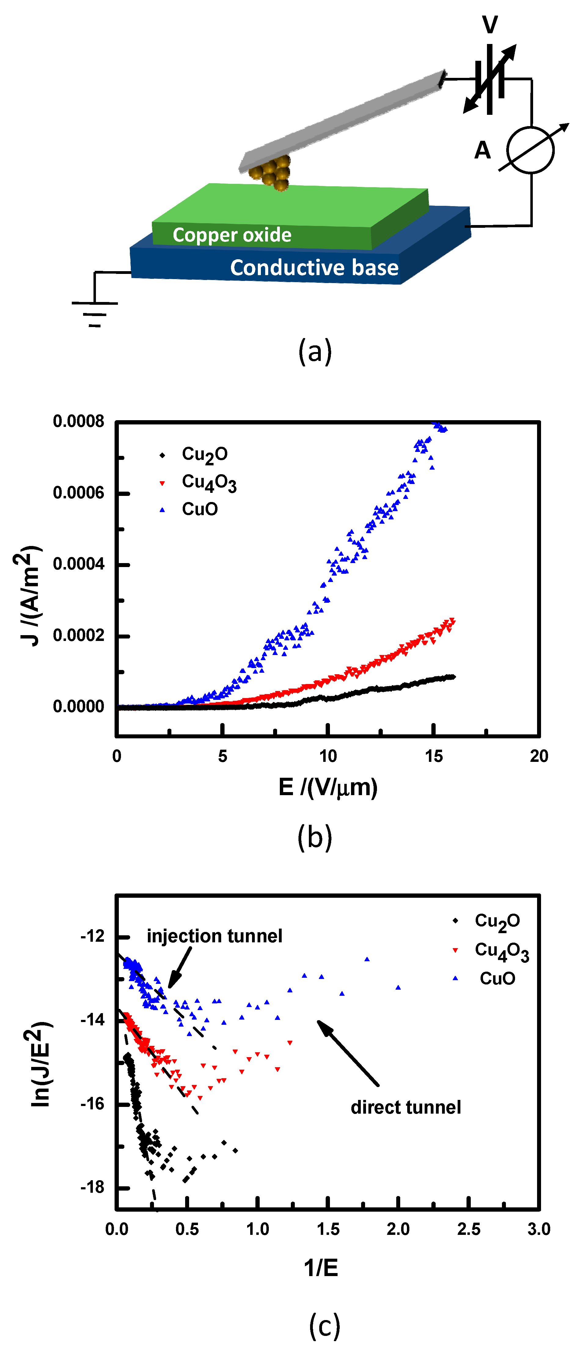
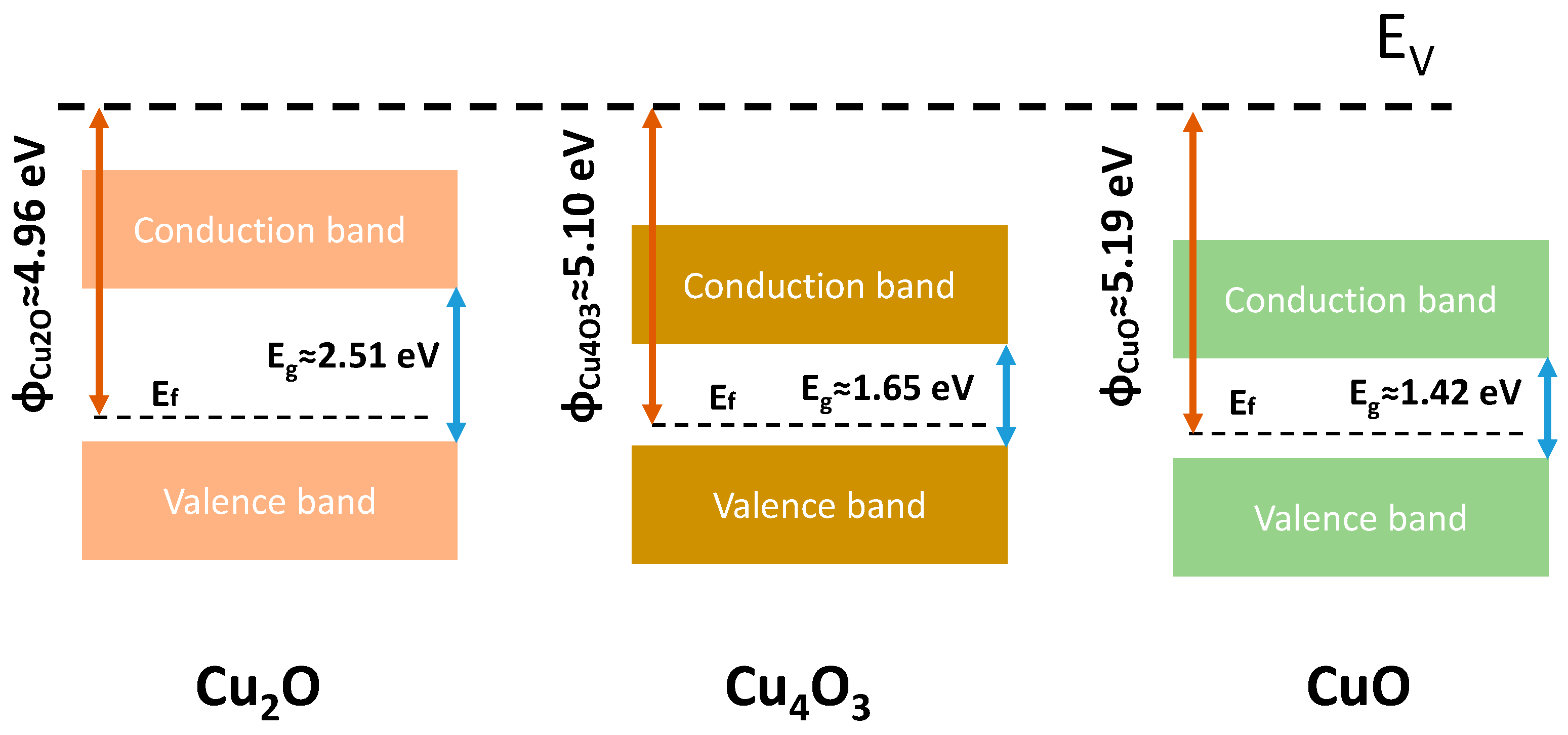
The Phase Evolution and Physical Properties of Binary Copper Oxide Thin Films Prepared by Reactive Magnetron Sputtering

Abstract
Share and Cite
Zheng, W.; Chen, Y.; Peng, X.; Zhong, K.; Lin, Y.; Huang, Z. The Phase Evolution and Physical Properties of Binary Copper Oxide Thin Films Prepared by Reactive Magnetron Sputtering. Materials 2018, 11, 1253. https://doi.org/10.3390/ma11071253
Zheng W, Chen Y, Peng X, Zhong K, Lin Y, Huang Z. The Phase Evolution and Physical Properties of Binary Copper Oxide Thin Films Prepared by Reactive Magnetron Sputtering. Materials. 2018; 11(7):1253. https://doi.org/10.3390/ma11071253
Chicago/Turabian StyleZheng, Weifeng, Yue Chen, Xihong Peng, Kehua Zhong, Yingbin Lin, and Zhigao Huang. 2018. "The Phase Evolution and Physical Properties of Binary Copper Oxide Thin Films Prepared by Reactive Magnetron Sputtering" Materials 11, no. 7: 1253. https://doi.org/10.3390/ma11071253
APA StyleZheng, W., Chen, Y., Peng, X., Zhong, K., Lin, Y., & Huang, Z. (2018). The Phase Evolution and Physical Properties of Binary Copper Oxide Thin Films Prepared by Reactive Magnetron Sputtering. Materials, 11(7), 1253. https://doi.org/10.3390/ma11071253