Morphological Evolution of Vertically Standing Molybdenum Disulfide Nanosheets by Chemical Vapor Deposition

 ,
, 
 ,
,
Abstract
:
1. Introduction
2. Materials and Methods
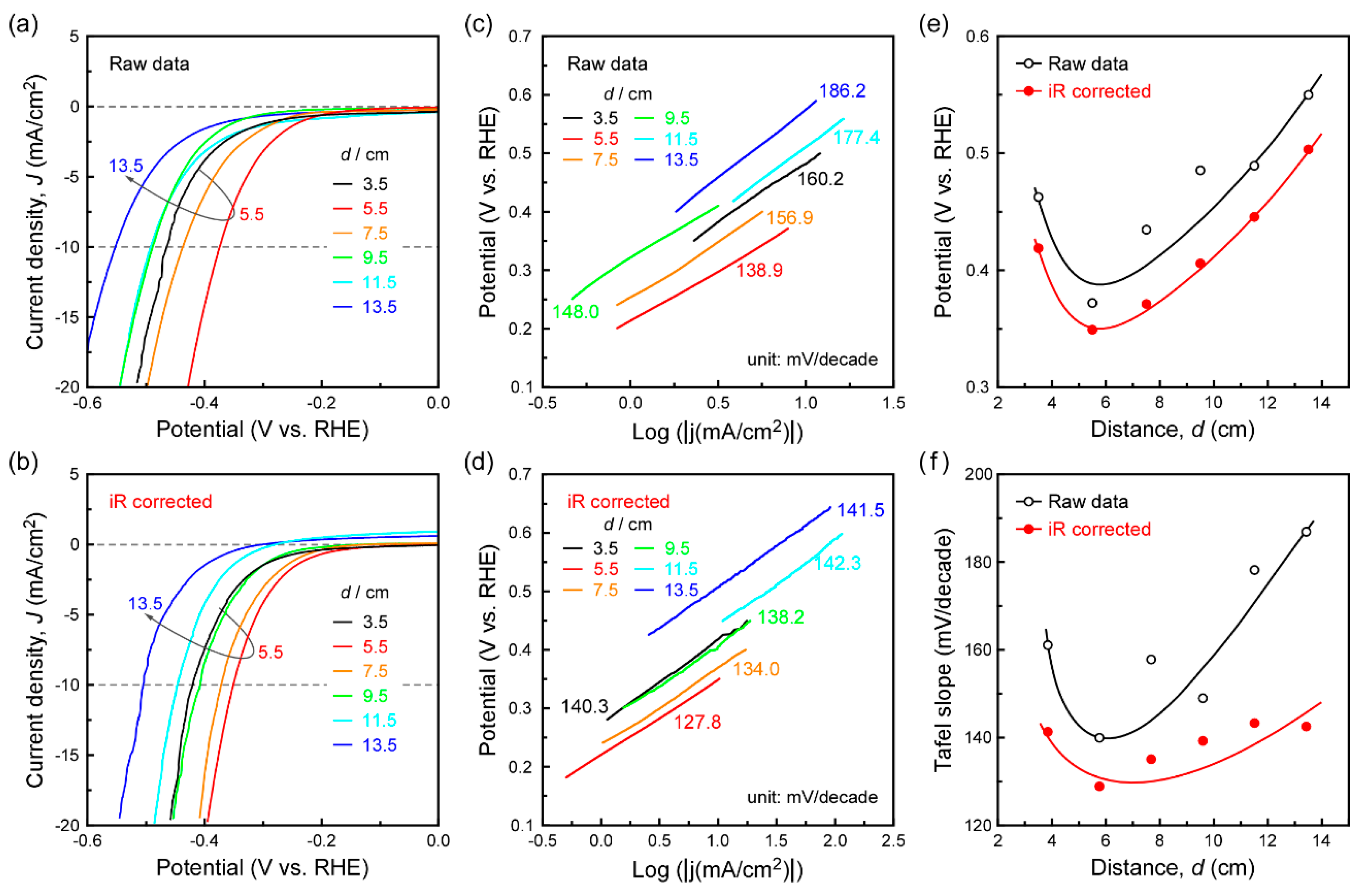
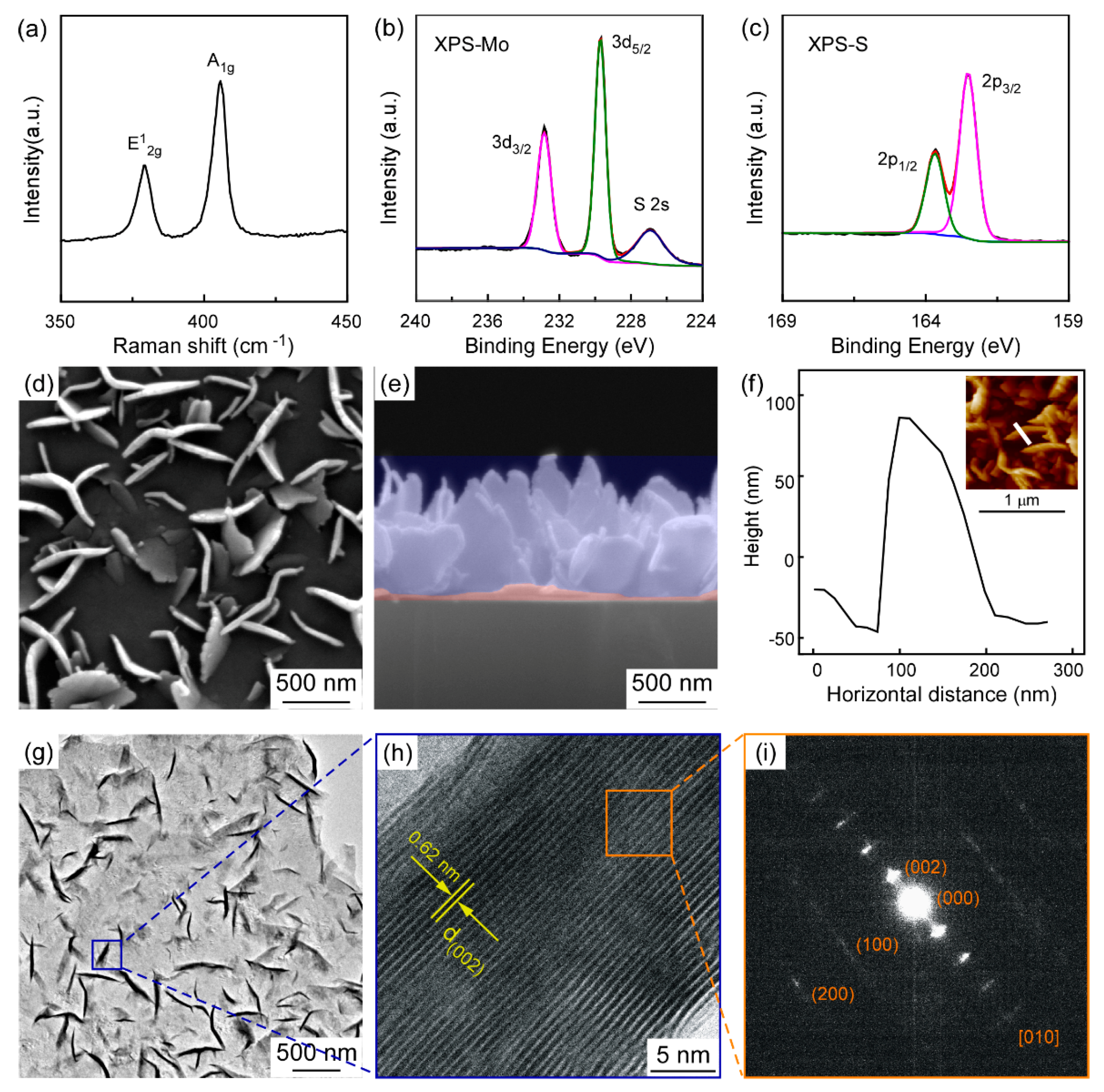
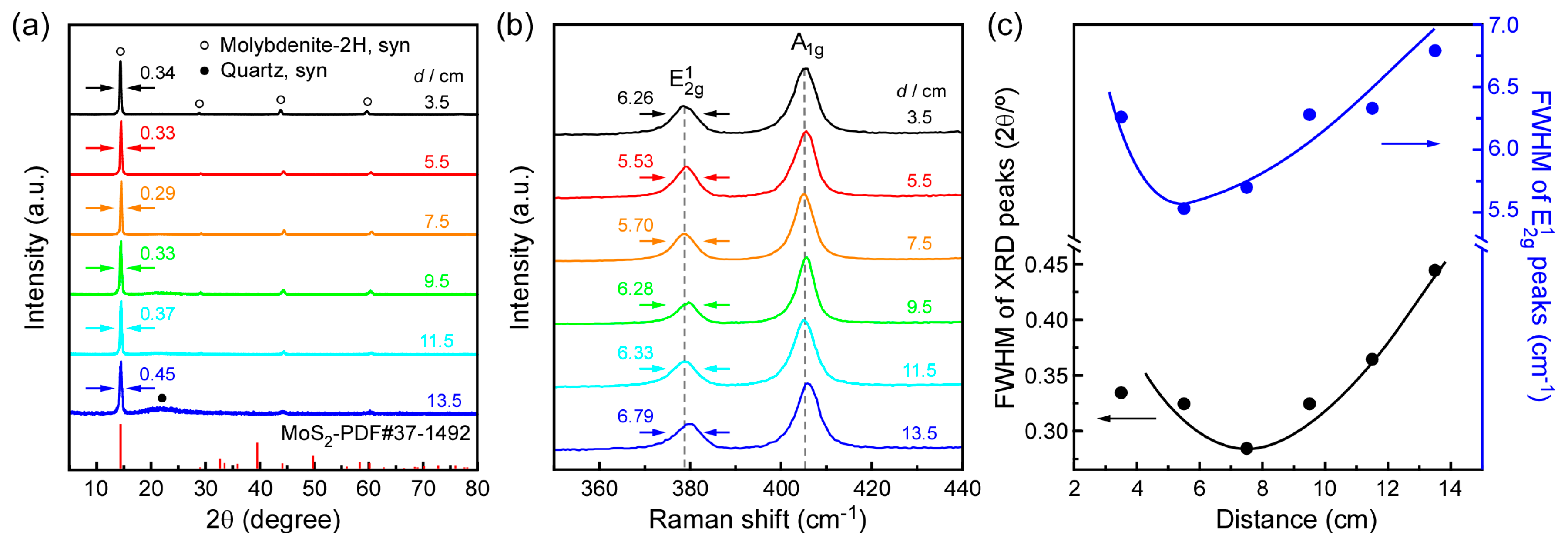
3. Results
4. Conclusions
Acknowledgments
Author Contributions
Conflicts of Interest
References
- Ji, Q.; Zhang, Y.; Zhang, Y.; Liu, Z. Chemical vapour deposition of group-VIB metal dichalcogenide monolayers: Engineered substrates from amorphous to single crystalline. Chem. Soc. Rev. 2015, 44, 2587–2602. [Google Scholar] [CrossRef] [PubMed]
- Remskar, M.; Mrzel, A.; Skraba, Z.; Jesih, A.; Ceh, M.; Demšar, J.; Stadelmann, P.; Lévy, F.; Mihailovic, D. Self-assembly of subnanometer-diameter single-wall MoS2 nanotubes. Science 2001, 292, 479–481. [Google Scholar] [CrossRef] [PubMed]
- Li, Q.; Walter, E.C.; van der Veer, W.E.; Murray, B.J.; Newberg, J.T.; Bohannan, E.W.; Switzer, J.A.; Hemminger, J.C.; Penner, R.M. Molybdenum disulfide nanowires and nanoribbons by electrochemical/chemical synthesis. J. Chem. Phys. B 2005, 109, 3169–3182. [Google Scholar] [CrossRef] [PubMed]
- Lv, R.; Robinson, J.A.; Schaak, R.E.; Sun, D.; Sun, Y.; Mallouk, T.E.; Terrones, M. Transition metal dichalcogenides and beyond: Synthesis, properties, and applications of single-and few-layer nanosheets. Acc. Chem. Res. 2015, 48, 56–64. [Google Scholar] [CrossRef] [PubMed]
- Jiang, S.; Yin, X.; Zhang, J.; Zhu, X.; Li, J.; He, M. Vertical ultrathin MoS2 nanosheets on a flexible substrate as an efficient counter electrode for dye-sensitized solar cells. Nanoscale 2015, 7, 10459–10464. [Google Scholar] [CrossRef] [PubMed]
- Li, H.; Wu, H.; Yuan, S.; Qian, H. Synthesis and characterization of vertically standing MoS2 nanosheets. Sci. Rep. 2016, 6, 21171. [Google Scholar] [CrossRef] [PubMed]
- Ling, L.; Wang, C.; Zhang, K.; Li, T.T.; Tang, L.; Li, C.W.; Wang, L.J.; Xu, Y.C.; Song, Q.J.; Yao, Y.G. Controlled growth of MoS2 nanopetals and their hydrogen evolution performance. RSC Adv. 2016, 6, 18483–18489. [Google Scholar] [CrossRef]
- Deokar, G.; Vignaud, D.; Arenal, R.; Louette, P.; Colomer, J.F. Modification of graphene oxide by laser irradiation: A new route to enhance antibacterial activity. Nanotechnology 2016, 27, 10. [Google Scholar]
- Wang, X.; Zhang, Z.; Chen, Y.; Qu, Y.; Lai, Y.; Li, J. Morphology-controlled synthesis of MoS2 nanostructures with different lithium storage properties. J. Alloys Compd. 2014, 600, 84–90. [Google Scholar] [CrossRef]
- Teng, Y.; Zhao, H.; Zhang, Z.; Li, Z.; Xia, Q.; Zhang, Y.; Zhao, L.; Du, X.; Du, Z.; Lv, P.; et al. MoS2 Nanosheets Vertically Grown on Graphene Sheets for Lithium-Ion Battery Anodes. ACS Nano 2016, 10, 8526–8535. [Google Scholar] [CrossRef] [PubMed]
- Deokar, G.; Rajput, N.S.; Vancso, P.; Ravaux, F.; Jouiad, M.; Vignaud, D.; Cecchet, F.; Colomer, J.F. Large area growth of vertically aligned luminescent MoS2 nanosheets. Nanoscale 2017, 9, 277–287. [Google Scholar] [CrossRef] [PubMed]
- Wu, Z.; Fang, B.; Wang, Z.; Wang, C.; Liu, Z.; Liu, F.; Wang, W.; Alfantazi, A.; Wang, D.; Wilkinson, D.P. MoS2 Nanosheets: A Designed Structure with High Active Site Density for the Hydrogen Evolution Reaction. ACS Catal. 2013, 3, 2101–2107. [Google Scholar] [CrossRef]
- Chhowalla, M.; Shin, H.S.; Eda, G.; Li, L.-J.; Loh, K.P.; Zhang, H. The chemistry of two-dimensional layered transition metal dichalcogenide nanosheets. Nat. Chem. 2013, 5, 263–275. [Google Scholar] [CrossRef] [PubMed]
- Kibsgaard, J.; Chen, Z.; Reinecke, B.N.; Jaramillo, T.F. Engineering the surface structure of MoS2 to preferentially expose active edge sites for electrocatalysis. Nat. Mater. 2012, 11, 963–969. [Google Scholar] [CrossRef] [PubMed]
- Li, S.; Wang, S.; Salamone, M.M.; Robertson, A.W.; Nayak, S.; Kim, H.; Tsang, S.C.E.; Pasta, M.; Warner, J.H. Edge-Enriched 2D MoS2 Thin Films Grown by Chemical Vapor Deposition for Enhanced Catalytic Performance. ACS Catal. 2017, 7, 877–886. [Google Scholar] [CrossRef]
- Zhang, Y.; Ji, Q.; Han, G.; Ju, J.; Shi, J.; Ma, D.; Sun, J. Dendritic, Transferable, Strictly Monolayer MoS2 Flakes Synthesized on SrTiO3 Single Crystals for Efficient Electrocatalytic Applications. ACS Nano 2014, 8, 8617–8624. [Google Scholar] [CrossRef] [PubMed]
- Lukowski, M.A.; Daniel, A.S.; Meng, F.; Forticaux, A.; Li, L.; Jin, S. Enhanced Hydrogen Evolution Catalysis from Chemically Exfoliated Metallic MoS2 Nanosheets. J. Am. Chem. Soc. 2013, 135, 10274–10277. [Google Scholar] [CrossRef] [PubMed]
- Yoo, Y.; Degregorio, Z.P.; Johns, J.E. Seed Crystal Homogeneity Controls Lateral and Vertical Heteroepitaxy of Monolayer MoS2 and WS2. J. Am. Chem. Soc. 2015, 137, 14281–14287. [Google Scholar] [CrossRef] [PubMed]
- Cao, Y.; Luo, X.; Yuan, C.; Han, S.; Yu, T.; Yang, Y.; Li, Q. Morphology engineering of monolayer MoS2 by adjusting chemical environment during growth. Phys. E Low Dimens. Syst. Nanostruct. 2015, 74, 292–296. [Google Scholar] [CrossRef]
- Cao, D.; Shen, T.; Liang, P.; Chen, X.; Shu, H. Role of Chemical Potential in Flake Shape and Edge Properties of Monolayer MoS2. J. Phys. Chem. C 2015, 119, 4294–4301. [Google Scholar] [CrossRef]
- Wang, S.S.; Rong, Y.M.; Fan, Y.; Pacios, M.; Bhaskaran, H.; He, K.; Warner, J.H. Shape Evolution of Monolayer MoS2 Crystals Grown by Chemical Vapor Deposition. Chem. Mater. 2014, 26, 6371–6379. [Google Scholar] [CrossRef]
- Cho, S.Y.; Kim, S.J.; Lee, Y.; Kim, J.S.; Jung, W.B.; Yoo, H.W.; Kim, J.; Jung, H.T. Highly Enhanced Gas Adsorption Properties in Vertically Aligned MoS2 Layers. ACS Nano 2015, 9, 9314–9321. [Google Scholar] [CrossRef] [PubMed]
- Wang, H.; Tsai, C.; Kong, D.; Chan, K.; Abild-pedersen, F.; Nørskov, J.K.; Cui, Y. Transition-metal doped edge sites in vertically aligned MoS2 catalysts for enhanced hydrogen evolution. Nano Res. 2015, 8, 566–575. [Google Scholar] [CrossRef]
- Zhou, Y.; Liu, Y.; Zhao, W.; Xie, F.; Xu, R.; Li, B.; Zhou, X.; Shen, H. Growth of vertically aligned MoS2 nanosheets on a Ti substrate through a self-supported bonding interface for high-performance lithium-ion batteries: A general approach. J. Mater. Chem. A 2016, 4, 5932–5941. [Google Scholar] [CrossRef]
- Bhimanapati, G.R.; Hankins, T.; Vila, R.A.; Yu, L.; Fuller, I.; Terrones, M.; Robinson, J.A. Growth and Tunable Surface Wettability of Vertical MoS2 Layers for Improved Hydrogen Evolution Reactions. ACS Appl. Mater. Interfaces 2016, 8, 22190–22195. [Google Scholar] [CrossRef] [PubMed]
- Shokhen, V.; Miroshnikov, Y.; Gershinsky, G.; Gotlib, N.; Stern, C.; Naveh, D.; Zitoun, D.; Ilan, B.; Bina, A.M.; Gan, R. On the impact of Vertical Alignment of MoS2 for Efficient Lithium Storage. Sci. Rep. 2017, 7, 3280. [Google Scholar] [CrossRef] [PubMed]
- Perkgoz, N.K.; Bay, M. Investigation of Single-Wall MoS2 Monolayer Flakes Grown by Chemical Vapor Deposition. Nano Micro Lett. 2016, 8, 70–79. [Google Scholar] [CrossRef]
- Zhang, Y.; Zhang, Y.; Ji, Q.; Ju, J.; Yuan, H.; Shi, J.; Gao, T.; Ma, D.; Liu, M.; Chen, Y.; et al. Controlled Growth of High-Quality Monolayer WS2 Layers on Sapphire and Imaging Its Grain Boundary. ACS Nano 2013, 7, 8963–8971. [Google Scholar] [CrossRef] [PubMed]
- Lin, Z.; Zhao, Y.; Zhou, C.; Zhong, R.; Wang, X.; Tsang, Y.H.; Chai, Y. Controllable Growth of Large–Size Crystalline MoS2 and Resist-Free Transfer Assisted with a Cu Thin Film. Sci. Rep. 2016, 5, 18596. [Google Scholar] [CrossRef] [PubMed]
- Duphil, D.; Bastide, S.; Lévy-Clément, C. Chemical Synthesis of Molybdenum Disulfide Nanoparticles in an Organic Solution. J. Mater. Chem. 2002, 12, 2430–2432. [Google Scholar] [CrossRef]
- Tao, H.; Yanagisawa, K.; Zhang, C.; Ueda, T.; Onda, A.; Li, N.; Shou, T. Synthesis and Growth Mechanism of Monodispersed MoS2 Sheets/Carbon Microspheres. CrystEngComm 2012, 14, 3027. [Google Scholar] [CrossRef]
- Kumar, V.K.; Dhar, S.; Choudhury, T.H.; Shivashankar, S.A.; Raghavan, S. A predictive approach to CVD of crystalline layers of TMDs: The case of MoS2. Nanoscale 2015, 7, 7802–7810. [Google Scholar] [CrossRef] [PubMed]
- Zhang, X.; Han, W.P.; Wu, J.B.; Milana, S.; Lu, Y.; Li, Q.Q.; Ferrari, A.C.; Tan, P.H. Raman spectroscopy of shear and layer breathing modes in multilayer MoS2. Phys. Rev. B 2013, 87, 115413. [Google Scholar] [CrossRef]
- Conley, H.J.; Wang, B.; Ziegler, J.I.; Haglund, R.F.; Pantelides, S.T.; Bolotin, K.I. Bandgap Engineering of Strained Monolayer and Bilayer MoS2. Nano Lett. 2013, 13, 3626–3630. [Google Scholar] [CrossRef] [PubMed]
- Jeong, S.; Shin, H.-Y.; Shin, R.H.; Jo, W.; Yoon, S.; Rübhausen, M. Raman scattering studies of the lattice dynamics in layered MoS2. J. Korean Phys. Soc. 2015, 66, 1575–1580. [Google Scholar] [CrossRef]
- Yang, Y.; Fei, H.; Ruan, G.; Xiang, C.; Tour, J.M. Edge-oriented MoS2 nanoporous films as flexible electrodes for hydrogen evolution reactions and supercapacitor devices. Adv. Mater. 2014, 26, 8163–8168. [Google Scholar] [CrossRef] [PubMed]
- Tan, S.M.; Ambrosi, A.; Sofer, Z.; Huber, Š.; Sedmidubský, D.; Pumera, M. Pristine Basal- and Edge-Plane-Oriented Molybdenite MoS2 Exhibiting Highly Anisotropic Properties. Chem. A Eur. J. 2015, 21, 7170–7178. [Google Scholar] [CrossRef] [PubMed]
- Fei, L.; Lei, S.; Zhang, W.B.; Lu, W.; Lin, Z.; Lam, C.H.; Chai, Y.; Wang, Y. Direct TEM observations of growth mechanisms of two-dimensional MoS2 flakes. Nat. Commun. 2016, 7, 12206. [Google Scholar] [CrossRef] [PubMed]
- Wang, J.; Chen, L.; Lu, W.; Zeng, M.; Tan, L.; Ren, F.; Jiang, C.; Fu, L. Direct growth of molybdenum disulfide on arbitrary insulating surfaces by chemical vapor deposition. RSC Adv. 2015, 5, 4364–4367. [Google Scholar] [CrossRef]
- Choi, Y.; Lee, J.; Parija, A.; Cho, J.; Verkhoturov, S.V.; Al-hashimi, M.; Fang, L.; Banerjee, S. An in Situ Sulfidation Approach for the Integration of MoS2 Nanosheets on Carbon Fiber Paper and the Modulation of Its Electrocatalytic Activity by Interfacing with nC60. ACS Catal. 2016, 6, 6246–6254. [Google Scholar] [CrossRef]
- Mos, R.L.; Fullerene-like, W.S.I. Atmospheric Pressure Chemical Vapor Deposition: An Alternative Route to Large-Scale MoS2 and WS2 Inorganic Fullerene-like Nanostructures and Nanoflowers. Chem. A Eur. J. 2004, 10, 6163–6171. [Google Scholar]
- Yu, Y.; Li, C.; Liu, Y.; Su, L.; Zhang, Y.; Cao, L. Controlled Scalable Synthesis of Uniform, High-Quality Monolayer and Few-layer MoS2 Films. Sci. Rep. 2013, 3, 1866. [Google Scholar] [CrossRef] [PubMed]
- Benck, J.D.; Hellstern, T.R.; Kibsgaard, J.; Chakthranont, P.; Jaramillo, T.F. Catalyzing the hydrogen evolution reaction (HER) with molybdenum sulfide nanomaterials. ACS Catal. 2014, 4, 3957–3971. [Google Scholar] [CrossRef]
- Conway, B.E.; Tilak, B.V. Interfacial processes involving electrocatalytic evolution and oxidation of H2, and the role of chemisorbed H. Electrochim. Acta 2002, 47, 3571–3594. [Google Scholar] [CrossRef]
- Tao, L.; Duan, X.; Wang, C.; Duan, X.; Wang, S. Plasma-engineered MoS2 thin-film as an efficient electrocatalyst for hydrogen evolution reaction. Chem. Commun. 2015, 51, 7470–7473. [Google Scholar] [CrossRef] [PubMed]
- Ji, Q.; Zhang, Y.; Shi, J.; Sun, J.; Zhang, Y.; Liu, Z. Morphological Engineering of CVD-Grown Transition Metal Dichalcogenides for Efficient Electrochemical Hydrogen Evolution. Adv. Mater. 2016, 28, 6207–6212. [Google Scholar] [CrossRef] [PubMed]
- Wang, H.; Zhang, Q.; Yao, H.; Liang, Z.; Lee, H.W.; Hsu, P.C.; Zheng, G.; Cui, Y. High Electrochemical Selectivity of Edge versus Terrace Sites in Two-Dimensional Layered MoS2 Materials. Nano Lett. 2014, 14, 7138–7144. [Google Scholar] [CrossRef] [PubMed]
- Shin, S.; Jin, Z.; Kwon, D.H.; Bose, R.; Min, Y.S. High Turnover Frequency of Hydrogen Evolution Reaction on Amorphous MoS2 Thin Film Directly Grown by Atomic Layer Deposition. Langmuir 2015, 31, 1196–1202. [Google Scholar] [CrossRef] [PubMed]
- Yan, Y.; Xia, B.; Li, N.; Xu, Z.; Fisher, A.; Wang, X.J. Vertically oriented MoS2 and WS2 nanosheets directly grown on carbon cloth as efficient and stable 3-dimensional hydrogen-evolving cathodes. Mater. Chem. A 2015, 3, 131–135. [Google Scholar] [CrossRef]


© 2018 by the authors. Licensee MDPI, Basel, Switzerland. This article is an open access article distributed under the terms and conditions of the Creative Commons Attribution (CC BY) license (http://creativecommons.org/licenses/by/4.0/).
Share and Cite
Zhang, S.; Liu, J.; Ruiz, K.H.; Tu, R.; Yang, M.; Li, Q.; Shi, J.; Li, H.; Zhang, L.; Goto, T. Morphological Evolution of Vertically Standing Molybdenum Disulfide Nanosheets by Chemical Vapor Deposition. Materials 2018, 11, 631. https://doi.org/10.3390/ma11040631
Zhang S, Liu J, Ruiz KH, Tu R, Yang M, Li Q, Shi J, Li H, Zhang L, Goto T. Morphological Evolution of Vertically Standing Molybdenum Disulfide Nanosheets by Chemical Vapor Deposition. Materials. 2018; 11(4):631. https://doi.org/10.3390/ma11040631
Chicago/Turabian StyleZhang, Song, Jiajia Liu, Karla Hernandez Ruiz, Rong Tu, Meijun Yang, Qizhong Li, Ji Shi, Haiwen Li, Lianmeng Zhang, and Takashi Goto. 2018. "Morphological Evolution of Vertically Standing Molybdenum Disulfide Nanosheets by Chemical Vapor Deposition" Materials 11, no. 4: 631. https://doi.org/10.3390/ma11040631
APA StyleZhang, S., Liu, J., Ruiz, K. H., Tu, R., Yang, M., Li, Q., Shi, J., Li, H., Zhang, L., & Goto, T. (2018). Morphological Evolution of Vertically Standing Molybdenum Disulfide Nanosheets by Chemical Vapor Deposition. Materials, 11(4), 631. https://doi.org/10.3390/ma11040631