Article

Low-Temperature CVD Graphene Nanostructures on Cu and Their Corrosion Properties

1
Department of Chemical and Materials Engineering, Chang Gung University, Taoyuan 33302, Taiwan
2
Department of Neurosurgery, Linkou Chang Gung Memorial Hospital, Taoyuan 33305, Taiwan
*
Author to whom correspondence should be addressed.
Materials 2018, 11(10), 1989; https://doi.org/10.3390/ma11101989
Submission received: 20 August 2018 / Revised: 2 October 2018 / Accepted: 2 October 2018 / Published: 15 October 2018
(This article belongs to the Special Issue Carbon Nanomaterials: Graphene, Nanoribbons and Quantum dots)

Abstract

:
Chemical vapor deposition (CVD) graphene is reported to effectively prevent the penetration of outer factors and insulate the underneath metals, hence achieving an anticorrosion purpose. However, there is little knowledge about their characteristics and corresponding corrosion properties, especially for those prepared under different parameters at low temperatures. Using electron cyclotron resonance chemical vapor deposition (ECR-CVD), we can successfully prepare graphene nanostructures on copper (Cu) at temperatures lower than 600 °C. Scanning electron microscopy (SEM), X-ray diffraction (XRD), Raman spectroscopy, and potentiodynamic polarization measurements were used to characterize these samples. In simulated seawater, i.e., 3.5 wt.% sodium chloride (NaCl) solution, the corrosion current density of one graphene-coated Cu fabricated at 400 °C can be 1.16 × 10⁻⁵ A/cm2, which is one order of magnitude lower than that of pure Cu. Moreover, the existence of tall graphene nanowalls was found not to be beneficial to the protection as a consequence of their layered orientation. These correlations among the morphology, structure, and corrosion properties of graphene nanostructures were investigated in this study. Therefore, the enhanced corrosion resistance in selected cases suggests that the low-temperature CVD graphene under appropriate conditions would be able to protect metal substrates against corrosion.

1. Introduction

Graphene has received numerous attentions since it was first detached from graphite through mechanical exfoliation and then used in a variety of applications [1,2,3,4,5,6,7,8,9,10,11,12,13,14,15]. Among all of the developed processes, chemical vapor deposition (CVD) is always viewed as an effective and powerful method for fabricating large-area and high-quality graphene. T J. Pang et al. discussed the CVD growth of one-dimensional (1D) and two-dimensional (2D) sp2 carbon nanomaterials, i.e., basically carbon nanotube and graphene, in 2015 [16]. Their growth mechanisms and dynamics were compared. Hofmann et al. reported on the chemical vapor deposition (CVD)-enabled graphene manufacture and technology in 2014 [17]. It mentioned the pressure and materials gap, the microstructure of CVD graphene films, and the catalyst−carbon phase diagram. Naghdi et al. reviewed the catalytic, catalyst-free, roll-to-roll, and low-temperature CVD growth of graphene in 2018 [18]. The role of the catalyst, carbon precursors, plasma assistance, catalyst-free, and roll-to-roll production all suggest that the research is still a long way from an economical and feasible approach for reducing the growth temperature. Chen et al. showed the scalable CVD growth of three-dimensional (3D) graphene materials in 2018 [19]. Graphene foams, graphene shells, hierarchical graphene, and their energy-related applications were presented. It is worthwhile to mention that few-layer epitaxial graphene nanowall arrays were able to be produced by microwave plasma-enhanced CVD with the help of thin SiC wall-like scaffolds [20].
On the other hand, graphene as an oxidation and corrosion resistive coating is of great interests recently [21,22,23,24,25,26,27,28,29,30]. For the oxidation resistance, Chen et al. showed this property of graphene-coated copper (Cu) and Cu/nickel (Ni) alloy against annealing at 200 °C in air [23]. Kalita et al. obtained graphene as an effective oxidation resistive barrier through the surface wave plasma CVD for against annealing at 150 °C in air [24]. Singh Raman et al. showed that graphene coating on Cu can increase the resistance to electrochemical degradation in 0.1 M of NaCl solution [25]. Prasai et al. reported on the corrosion-inhibiting graphene coating in Na2SO4 solution [26]. Hsieh et al. achieved the complete corrosion inhibition through graphene defect passivation using atomic layer deposition (ALD) [27]. Miskovic-Stankovic et al. indicated that graphene coating on Cu showed better protective properties than that on Al in 0.1 M of NaCl solution [28]. In contrast, Dong et al. claimed that the graphene film did not effectively protect Cu in the prolonged exposure to 3.5 wt.% NaCl solution [29]. Furthermore, Qi et al. synthesized the polymethylmethacrylate (PMMA)-grafted graphene oxide coating, which can prevent the corrosion of Cu in a 3.5 wt.% NaCl solution [30]. However, there is little information available on low-temperature chemical vapor deposition (LTCVD) graphene nanostructures and their electrochemical anticorrosion properties. Nevertheless, the high process temperatures may induce the phase transformation of various metal substrates and generate unnecessary changes in their mechanical as well as other properties, even only within a short time. On the other hand, to the best of our knowledge, there is no such study, and it is very difficult to achieve good coverage and high-quality graphene through low-temperature CVD with improved anticorrosion properties at the same time. Therefore, in this study, we prepared the CVD graphene-coated Cu substrates at and below 600 °C, and further investigated their electrochemical properties in a 3.5 wt.% NaCl solution. It is hoped that the information from this study would be useful for the development and design of novel anticorrosion coatings based on 2D materials.

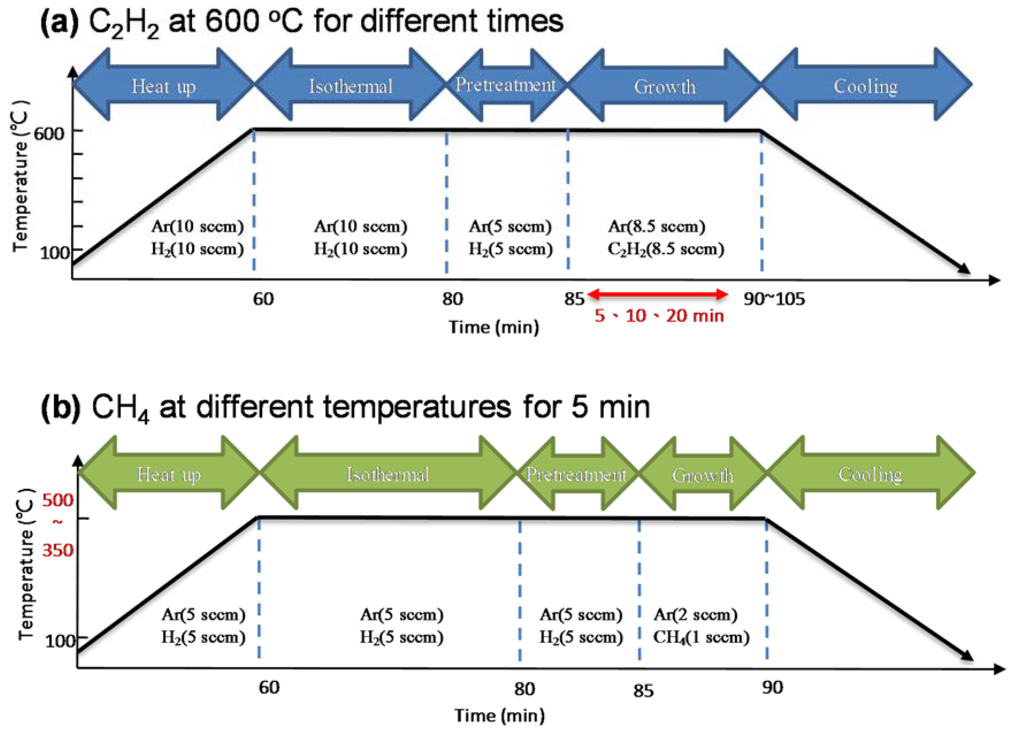
2. Materials and Methods

Cu foils (30 cm × 150 cm × 0.00254 cm) were obtained from Alfa Aesar (Lancashire, UK). Ag paste (OP-915, Double-O Technology Co., Ltd. Taipei, Taiwan) and pipe sealant (Loctite 5331, Henkel AG & Company, KGaA, Dusseldorf, Germany) were purchased for electrochemical measurements. A multi-sources electron cyclotron resonance chemical vapor deposition system (MECR-CVD, Industrial Technology Research Institute (ITRI), Hsinchu, Taiwan) was used for growing graphene films through flowing C2H2 at 600 °C for different times. On the other hand, electron cyclotron resonance chemical vapor deposition system (ECR-CVD, Industrial Technology Research Institute (ITRI), Hsinchu, Taiwan) was used for growing graphene films through flowing CH4 at different temperatures for 5 min. For film growth, the Cu foil (area: 2 cm × 2 cm) was used at the microwave power of 1200 W. The detailed rest process conditions and parameters were listed in Scheme 1. Since the MECR-CVD chamber is bigger than that of the ECR-CVD, we used a higher flow rate of precursor gases. After the pretreatment process, we used a gate valve to control the process pressures.
For material analyses, a field-emission scanning electron microscope (JEOL, JSM-7500F, Tokyo, Japan) and an X-ray diffractometer (Bruker, D2 Phaser, Billerica, MA, United States) were adopted. In addition, the graphene films on the Cu substrate were checked by a micro-Raman spectrometer (RAMaker Protrustech Co., Ltd. Tainan, Taiwan). Potentiodynamic polarization measurements were carried out by using a CHI potentiostat system (CHI 7032D, CH Instruments, Inc., Austin, TX, USA) in a typical three-electrode setup with an Ag/AgCl reference electrode and a Pt wire counter electrode. For preparing the working electrode, the Cu wire was mounted on the backside of Cu substrates through silver paste, while the backside and surrounding sides were protected by pipe sealant. The drying conditions of the silver paste and pipe sealant are 80 °C for 3.5 h and 40 °C for 30 min, respectively. The electrolyte is 3.5 wt.% NaCl solution, and the sweeping potential range is between −0.8 and 0.6 V at the scan rate of 10 mV/s. All of the solutions were prepared with deionized water with a resistivity of more than 18 megohm/cm. We used CorrView software (version 2.6) to do data fitting in the Tafel plot in order to get the corrosion potential.

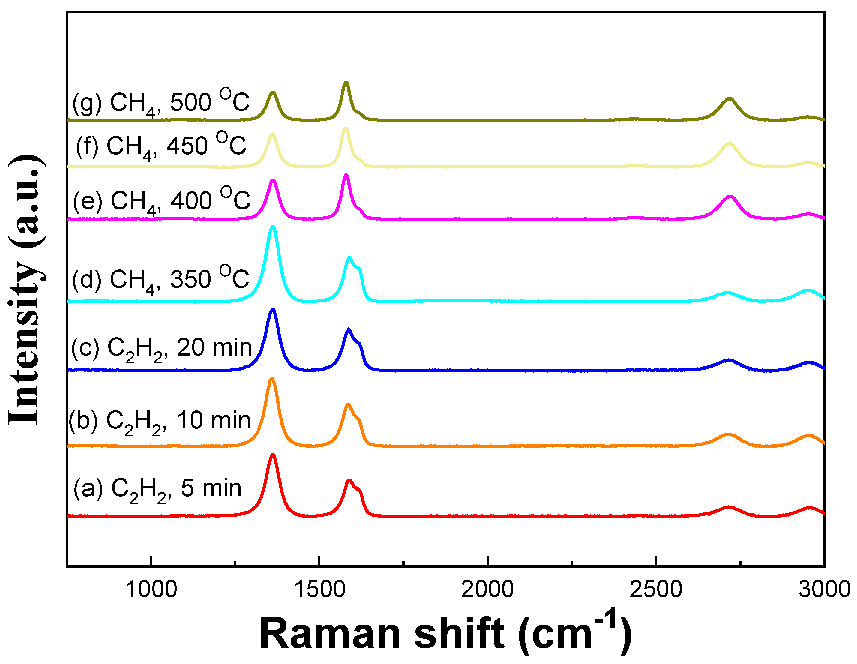
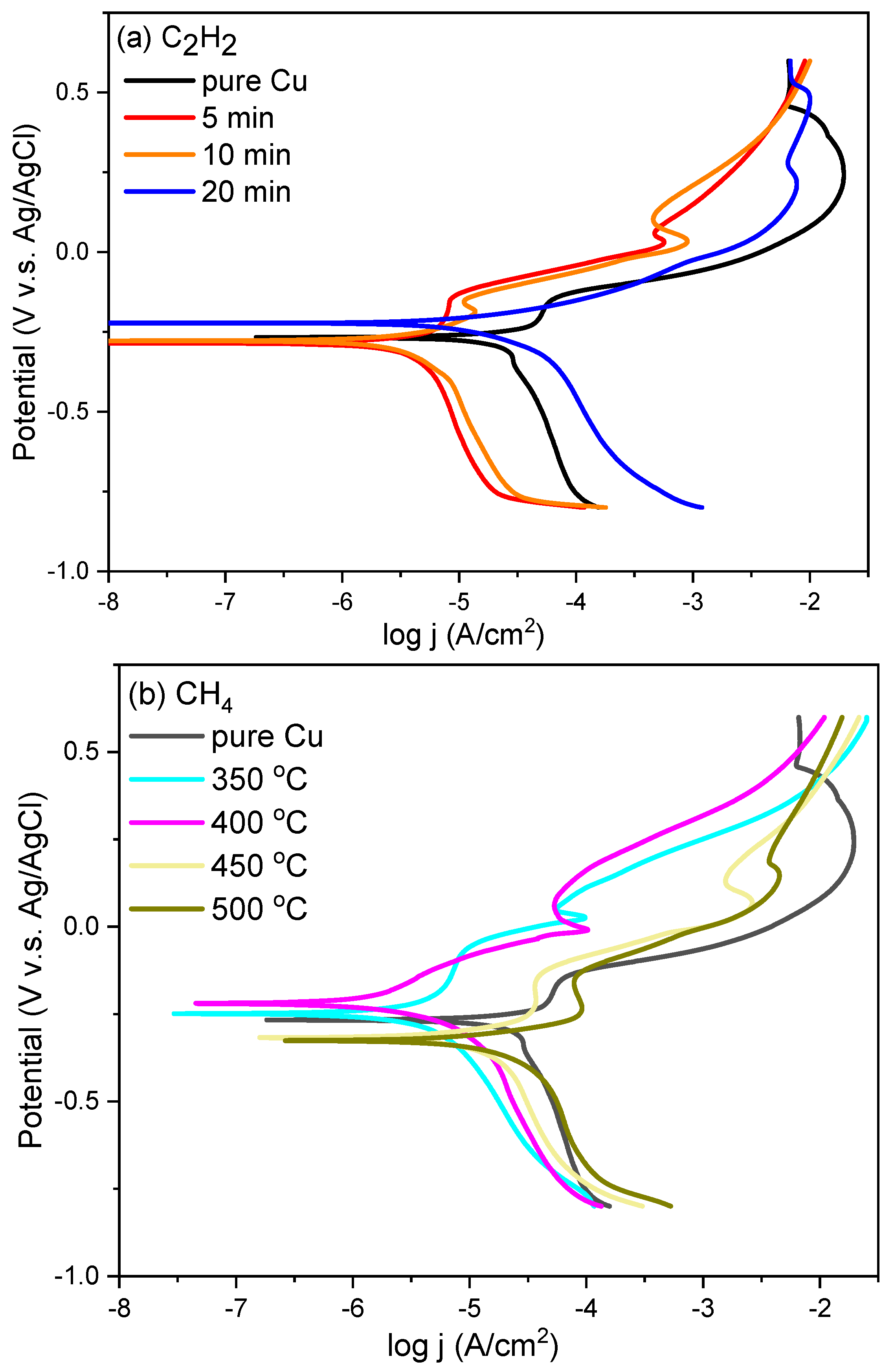
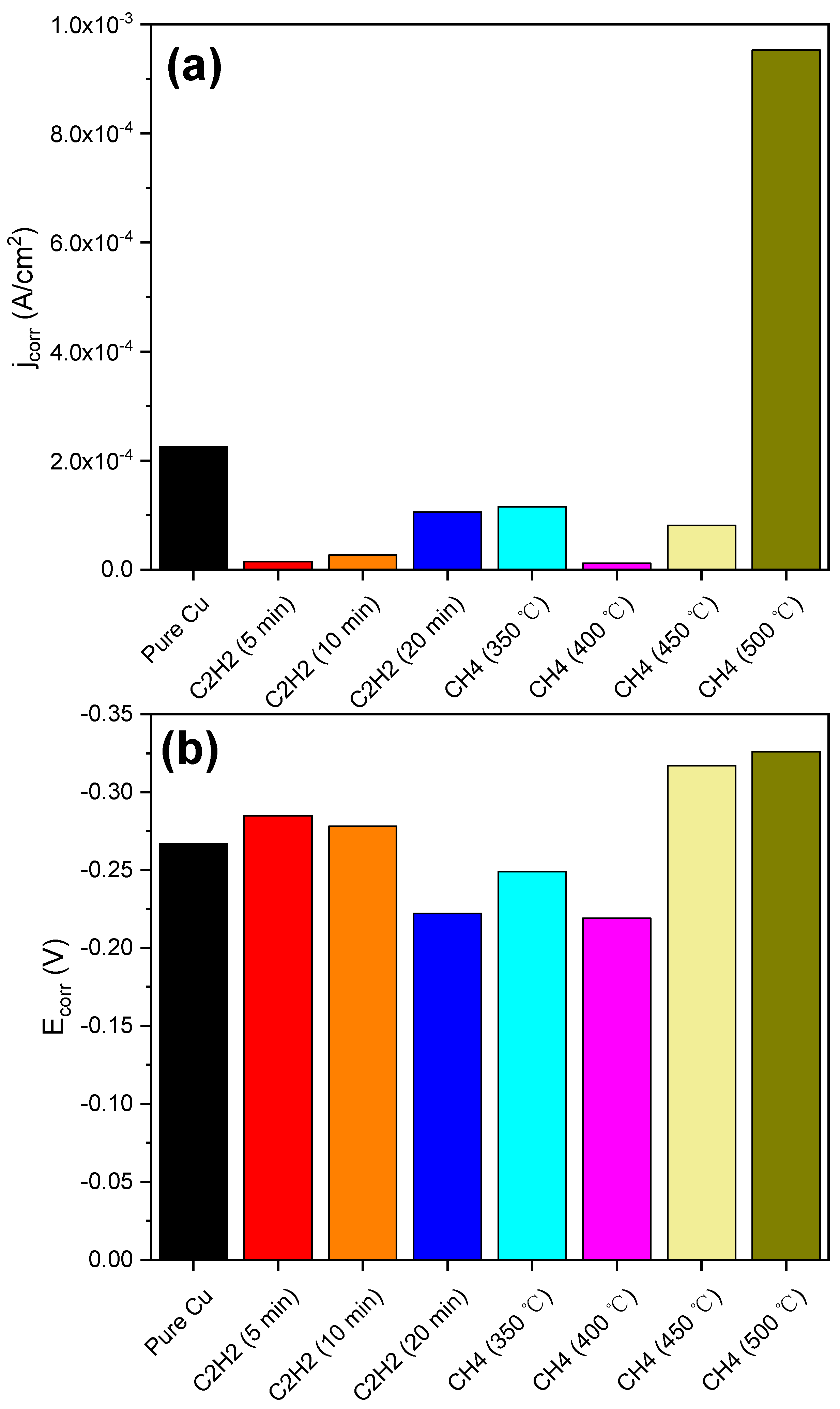
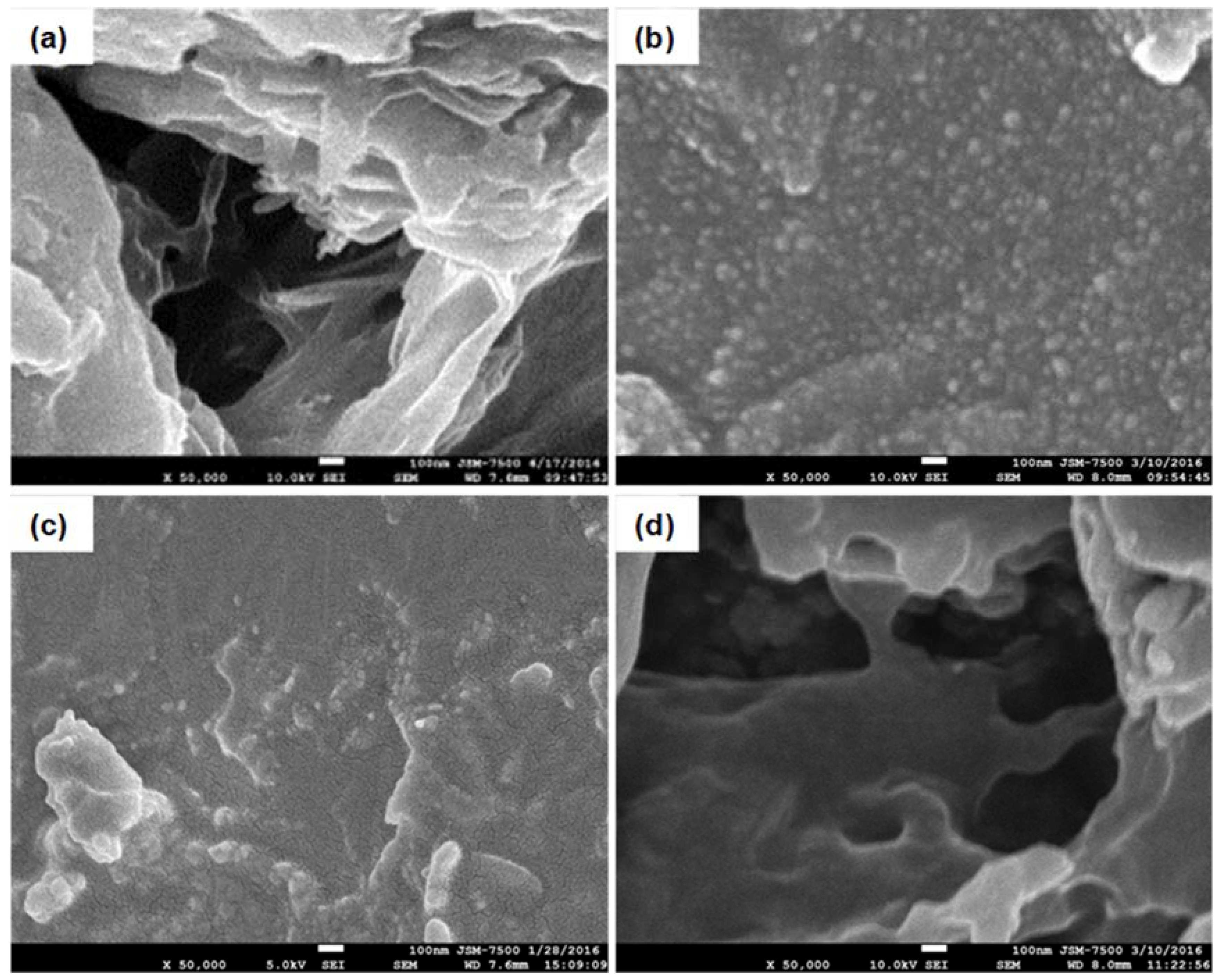
3. Results and Discussion

Figure 1 shows the Scanning electron microscopy (SEM) pictures before the electrochemical corrosion experiments. Before the CVD growth, the Cu foil surface is relatively dark and smooth. After the CVD growth, the foil surface becomes bright and rough, with the existence of either graphene films or nanowalls. Figure 1b–d illustrates the surface morphologies with a variety of growth atmospheres, temperatures, and conditions. In Figure 1b, through the growth at 600 °C for 5 min with C2H2 flow, the surface texture seems not that clear, with few relatively large spots on gray surface. Figure 1c,d is picture through the growth at 350 °C and 500 °C for 5 min with CH4 flow, respectively. In the beginning, some rectangular stereostructures appear randomly at 350 °C, and gradually become larger through increasing temperatures, finally form the graphene nanowalls at 500 °C. In the later stages, even rose-like or flower-like structures start to stack and form big spheres under the influence of growth conditions. In general, graphene films grow for the most part in width, and not in height. While the film is thin, this coating appears flat. With a further increase in the amount of material in the film, it gets pinched and forms a texture. Figure 1e,f is the X-ray diffraction (XRD) patterns for samples with a variety of growth atmospheres, temperatures, and conditions. The two theta angles were from 10 to 70 degrees, and we ignored between 45–52 degrees, so that the strong signals from the Cu foil substrates did not interfere. It was found that there is a small and broad peak ranging from 20 to 30 degrees in both patterns. It could correspond to the graphite (002) peak located at 26.53 degrees (PDF card 00-056-0159). The relatively smaller full width at half maximum (FWHM) of Figure 1e than that of Figure 1f indicates that a larger grain along the c axis and better crystallinity for the growth at 600 °C with C2H2 flow. These large grain and good crystallinity would be attributed to the high growth temperature and better horizontal coverage. On the other hand, because the carbon ratio of C2H2 is higher than CH4, the C2H2 precursor could get more C2 radicals, which might be helpful for film deposition.
Figure 2a–g is the Raman spectra for samples with a variety of growth atmospheres, temperatures, and conditions with the laser excitation wavelength of 473 nm. There are Raman peaks at 1350 cm−1 (D band), 1590 cm−1 (G band), 1620 cm−1 (D′ band), 2690 cm−1 (2D band), and 2950 cm−1 (D + G band). These peaks concur the existence of graphene films and nanowalls on Cu foil substrates that are observed in the above SEM and XRD analyses. First, the small 2D peaks imply multilayer graphene structure for all of the cases instead of a few-layer or even a single-layer structure. For the Figure 2a–c with C2H2 flow, the growth time is the parameter that we controlled at the same temperature of 600 °C. The decreasing ID/IG ratios are 1.70, 1.60, and 1.47 as a result of the better crystallinity for long growth times. For the Figure 2d−g with CH4 flow, the growth temperatures are 350 °C, 400 °C, 450 °C, and 500 °C with the same time of 5 min. In Table 1, the decreasing ID/IG ratios are 1.69, 0.87, 0.84 and 0.72 for the increasing growth temperatures. Here, the high G-band intensity at higher growth temperatures is due to the much superior sp2 crystallization of graphene nanostructures compared with that of 300 °C. Especially, there is a rapid transition from 350 °C to 400 °C, and the finally forming non-flat and porous graphene nanowalls at 500 °C.
Figure 3 indicates the potentiodynamic polarization curves of the first scan for pure, CVD graphene (C2H2, 5 min)-coated, and CVD graphene (CH4, 350 °C)-coated Cu foils. The experiments were carried out ranging from −0.8 V to 0.6 V v.s. Ag/AgCl at the scan rate of 10 mV/s at room temperature. Originally, the corrosion potential for pure Cu foil is around −0.267 V. After adding good CVD graphene coatings, the corrosion potentials are shifted toward −0.2 V with several tens mV with relatively low corrosion activities. It depicts that the suitable CVD graphene coatings are able to improve the anticorrosion property under the appropriate growth conditions. Figure 4a,b is the summary of electrochemical corrosion current densities (jcorr) and corrosion potential (Ecorr) for the first scan. In addition, the scan numbers were raised 30 times in order to investigate the long-term stability. The corrosion current densities (jcorr) and corrosion potentials (Ecorr) for CVD graphene (C2H2)-coated Cu foils at different growth times and pure Cu foil were displayed in the left-hand side of Figure 4a,b, respectively. The jcorr of all of the CVD graphene (C2H2)-coated ones are lower than that of pure Cu foil. It is worthwhile to mention that the Ecorr for graphene (C2H2, 20 min) is closer to the positive side with lower jcorr, although it is relatively higher than those with shorter growth times. The right-hand side of Figure 4a,b illustrated the jcorr and Ecorr for CVD graphene (CH4)-coated Cu foils at different growth temperatures and pure Cu foil, respectively. Despite the curve for 500 °C, all of the remaining jcorr are lower than that of pure Cu foil. However, the Ecorr for graphene (CH4, 450 °C and 500 °C)-coated Cu foils are closed to the more negative potentials. This indicates that the appearance of vertical structures of graphene nanowalls might be fatal to the protection as a consequence of the fast diffusion channel against the horizontal surface. Among all of the growth conditions, the champion film is CVD graphene (CH4, 400 °C, 5 min), and its jcorr and Ecorr are 1.16 × 10⁻⁵ A/cm2 and −0.219 V. Therefore, it is claimed that the protection graphene nanostructure can be successfully achieved at a relatively low temperature of 400 °C for 5 min in our system.
Figure 5a–d show the SEM pictures after the electrochemical corrosion experiments. After washing surfaces using the deionized water, all of the surfaces are not as flat as those before the electrochemical measurements. As shown in Figure 5a,d, some micrometer-size holes start to appear on pure and CVD graphene (CH4, 500 °C)-coated Cu foils. Hence, basically the porous and high graphene nanowalls do not help the protection against corrosion in terms of morphology. In contrast, the surface with a low CVD growth temperature of 350 °C seems better. Figure 5b demonstrates the flattest surface with CVD graphene (C2H2, 5 min) coating. This flatness is correlated with the relatively low jcorr and Ecorr on the more positive potential side. It indicates that the intermediate temperature CVD graphene with C2H2 as the carbon source can form the complete protection layer in a short growth time of five minutes, even suffering from multiple scans. Still, the corrosion will cause the surface oxidation confirmed by comparing the energy-dispersive x-ray spectroscopy (EDS) spectra (Figure S1 in Supplementary Materials). Similar trends can be found for graphene (CH4, 350 °C) and graphene (CH4, 400 °C) coatings. However, after 10 scans, the Ecorr of pure Cu will shift to around −0.16 V, which could be a consequence of forming a passivation layer and thus be higher than those of all of the graphene-coated ones.

4. Conclusions

In conclusion, we have successfully demonstrated LTCVD graphene nanostructures with promising anticorrosion characteristics. The low jcorr and Ecorr closed to the more positive side of graphene-coated Cu can be achieved simultaneously for selected and optimal cases. More importantly, the lowest jcorr of graphene (CH4, 400 °C)-coated Cu is one order of magnitude lower than that of the pure Cu. Meanwhile, its Ecorr of −0.219 V is 52 mV more positive than that of unmodified Cu. In contrast, the cases located outside the appropriate process window may suffer from non-uniform coverage, poor crystallinity, or porous nanowall structures, which also provide vertical diffusion pathway into the substrates. Our study suggests that the appropriate process and associated structures are essential to the development of graphene-based anticorrosion coatings through LTCVD.

Supplementary Materials

The following are available online at https://www.mdpi.com/1996-1944/11/10/1989/s1, Figure S1: EDS spectra of CVD graphene (C2H2, 600 °C, 5 min) coatings before and after electrochemical corrosion experiments. Time-dependent Jcorr and Ecorr in the samples, Figure S2: Time-dependent Jcorr and Ecorr in these samples.

Author Contributions

Conceptualization, C.-L.S.; Methodology, W.-H.H.; Experiment, W.-H.H.; Formal Analysis, W.-H.H. and C.-H.L.; Resources, C.-L.S.; Writing-Original Draft Preparation, W.-H.H. and B.-S.L.; Writing-Review & Editing, C.-H.L. and C.-L.S.; Supervision, C.-L.S.; Funding Acquisition, C.-L.S.

Funding

This research was funded by Ministry of Science and Technology, Chang Gung University and Chang Gung Memorial Hospital under the grant numbers of BMRPA64, CMRPD3E0361, and CMRPD3E0362.

Acknowledgments

The authors would like to thank Ministry of Science and Technology, Chang Gung University and Chang Gung Memorial Hospital for the financial support.

Conflicts of Interest

The authors declare no conflict of interest.

References

  1. Novoselov, K.S.; Geim, A.K.; Morozov, S.V.; Jiang, D.; Zhang, Y.; Dubonos, S.V.; Grigorieva, I.V.; Firsov, A.A. Electric Field Effect in Atomically Thin Carbon Films. Science 2004, 306, 666–669. [Google Scholar] [CrossRef] [PubMed] [Green Version]
  2. Novoselov, K.S.; Geim, A.K.; Morozov, S.V.; Jiang, D.; Katsnelson, M.I.; Grigorieva, I.V.; Dubonos, S.V.; Firsov, A.A. Two-dimensional gas of massless Dirac fermions in graphene. Nature 2005, 438, 197–200. [Google Scholar] [CrossRef] [PubMed] [Green Version]
  3. Su, C.Y.; Lu, A.Y.; Wu, C.Y.; Li, Y.T.; Liu, K.K.; Zhang, W.; Lin, S.Y.; Juang, Z.Y.; Zhong, Y.L.; Chen, F.R.; et al. Direct formation of wafer scale graphene thin layers on insulating substrates by chemical vapor deposition. Nano Lett. 2011, 11, 3612–3616. [Google Scholar] [CrossRef] [PubMed]
  4. Su, C.Y.; Lu, A.Y.; Xu, Y.; Chen, F.R.; Khlobystov, A.N.; Li, L.J. High-quality thin graphene films from fast electrochemical exfoliation. ACS Nano 2011, 5, 2332–2339. [Google Scholar] [CrossRef] [PubMed]
  5. Sun, C.L.; Lee, H.H.; Yang, J.M.; Wu, C.C. The simultaneous electrochemical detection of ascorbic acid, dopamine, and uric acid using graphene/size-selected Pt nanocomposites. Biosens. Bioelectron. 2011, 26, 3450–3455. [Google Scholar] [CrossRef] [PubMed]
  6. Hsu, Y.-W.; Hsu, T.-K.; Sun, C.-L.; Nien, Y.-T.; Pu, N.-W.; Ger, M.-D. Synthesis of CuO/graphene nanocomposites for nonenzymatic electrochemical glucose biosensor applications. Electrochim. Acta 2012, 82, 152–157. [Google Scholar] [CrossRef]
  7. Yeh, M.-H.; Sun, C.-L.; Su, J.-S.; Lin, L.-Y.; Lee, C.-P.; Chen, C.-Y.; Wu, C.-G.; Vittal, R.; Ho, K.-C. A low-cost counter electrode of ITO glass coated with a graphene/Nafion® composite film for use in dye-sensitized solar cells. Carbon 2012, 50, 4192–4202. [Google Scholar] [CrossRef]
  8. Sun, C.-L.; Cheng, W.-L.; Hsu, T.-K.; Chang, C.-W.; Chang, J.-L.; Zen, J.-M. Ultrasensitive and highly stable nonenzymatic glucose sensor by a CuO/graphene-modified screen-printed carbon electrode integrated with flow-injection analysis. Electrochem. Commun. 2013, 30, 91–94. [Google Scholar] [CrossRef]
  9. Wang, L.; Yang, R.T.; Sun, C.-L. Graphene and other carbon sorbents for selective adsorption of thiophene from liquid fuel. AICHE J. 2013, 59, 29–32. [Google Scholar] [CrossRef]
  10. Sun, C.-L.; Su, J.-S.; Tang, J.-H.; Lin, M.-C.; Wu, J.-J.; Pu, N.-W.; Shi, G.-N.; Ger, M.-D. Investigation of the adsorption of size-selected Pt colloidal nanoparticles on high-surface-area graphene powders for methanol oxidation reaction. J. Taiwan Inst. Chem. Eng. 2014, 45, 1025–1030. [Google Scholar] [CrossRef]
  11. Yang, J.-M.; Wang, S.-A.; Sun, C.-L.; Ger, M.-D. Synthesis of size-selected Pt nanoparticles supported on sulfonated graphene with polyvinyl alcohol for methanol oxidation in alkaline solutions. J. Power Source 2014, 254, 298–305. [Google Scholar] [CrossRef]
  12. Sun, C.-L.; Tang, J.-S.; Brazeau, N.; Wu, J.-J.; Ntais, S.; Yin, C.-W.; Chou, H.-L.; Baranova, E.A. Particle size effects of sulfonated graphene supported Pt nanoparticles on ethanol electrooxidation. Electrochim. Acta 2015, 162, 282–289. [Google Scholar] [CrossRef]
  13. Pu, N.-W.; Shi, G.-N.; Liu, Y.-M.; Sun, X.; Chang, J.-K.; Sun, C.-L.; Ger, M.-D.; Chen, C.-Y.; Wang, P.-C.; Peng, Y.-Y.; et al. Graphene grown on stainless steel as a high-performance and ecofriendly anti-corrosion coating for polymer electrolyte membrane fuel cell bipolar plates. J. Power Source 2015, 282, 248–256. [Google Scholar] [CrossRef]
  14. Liu, B.; Liu, Z.; Chiu, I.S.; Di, M.; Wu, Y.; Wang, J.C.; Hou, T.H.; Lai, C.S. Programmable Synaptic Metaplasticity and below Femtojoule Spiking Energy Realized in Graphene-Based Neuromorphic Memristor. ACS Appl. Mater. Interfaces 2018, 10, 20237–20243. [Google Scholar] [CrossRef] [PubMed]
  15. Liu, X.; Ye, C.; Li, X.; Cui, N.; Wu, T.; Du, S.; Wei, Q.; Fu, L.; Yin, J.; Lin, C.T. Highly Sensitive and Selective Potassium Ion Detection Based on Graphene Hall Effect Biosensors. Materials 2018, 11, 399. [Google Scholar] [CrossRef] [PubMed]
  16. Pang, J.; Bachmatiuk, A.; Ibrahim, I.; Fu, L.; Placha, D.; Martynkova, G.S.; Trzebicka, B.; Gemming, T.; Eckert, J.; Rümmeli, M.H. CVD growth of 1D and 2D sp2 carbon nanomaterials. J. Mater. Sci. 2016, 51, 640–667. [Google Scholar] [CrossRef]
  17. Hofmann, S.; Braeuninger-Weimer, P.; Weatherup, R.S. CVD-Enabled Graphene Manufacture and Technology. J. Phys. Chem. Lett. 2015, 6, 2714–2721. [Google Scholar] [CrossRef] [PubMed]
  18. Naghdi, S.; Rhee, K.Y.; Park, S.J. A catalytic, catalyst-free, and roll-to-roll production of graphene via chemical vapor deposition: Low temperature growth. Carbon 2018, 127, 1–12. [Google Scholar] [CrossRef]
  19. Chen, K.; Shi, L.; Zhang, Y.; Liu, Z. Scalable chemical-vapour-deposition growth of three-dimensional graphene materials towards energy-related applications. Chem. Soc. Rev. 2018, 47, 3018–3036. [Google Scholar] [CrossRef] [PubMed]
  20. Hu, M.-S.; Kuo, C.-C.; Wu, C.-T.; Chen, C.-W.; Ang, P.K.; Loh, K.P.; Chen, K.-H.; Chen, L.-C. The production of SiC nanowalls sheathed with a few layers of strained graphene and their use in heterogeneous catalysis and sensing applications. Carbon 2011, 49, 4911–4919. [Google Scholar] [CrossRef]
  21. Parra, C.; Montero-Silva, F.; Gentil, D.; Del Campo, V.; Henrique Rodrigues da Cunha, T.; Henriquez, R.; Haberle, P.; Garin, C.; Ramirez, C.; Fuentes, R.; et al. The Many Faces of Graphene as Protection Barrier. Performance under Microbial Corrosion and Ni Allergy Conditions. Materials 2017, 10, 1406. [Google Scholar] [CrossRef] [PubMed]
  22. Li, S.; Hou, B.; Dai, D.; Shu, S.; Wu, M.; Li, A.; Han, Y.; Zhu, Z.-X.; Chen, B.-A.; Ding, Y.; et al. CVD Synthesis of Monodisperse Graphene/Cu Microparticles with High Corrosion Resistance in Cu Etchant. Materials 2018, 11, 1459. [Google Scholar] [CrossRef] [PubMed]
  23. Chen, S.; Brown, L.; Levendorf, M.; Cai, W.; Ju, S.Y.; Edgeworth, J.; Li, X.; Magnuson, C.W.; Velamakanni, A.; Piner, R.D.; et al. Oxidation Resistance of Graphene-Coated Cu and Cu-Ni Alloy. ACS Nano 2011, 5, 1321–1327. [Google Scholar] [CrossRef] [PubMed]
  24. Kalita, G.; Ayhan, M.E.; Sharma, S.; Shinde, S.M.; Ghimire, D.; Wakita, K.; Umeno, M.; Tanemura, M. Low temperature deposited graphene by surface wave plasma CVD as effective oxidation resistive barrier. Corros. Sci. 2014, 78, 183–187. [Google Scholar] [CrossRef]
  25. Singh Raman, R.K.; Chakraborty Banerjee, P.; Lobo, D.E.; Gullapalli, H.; Sumandasa, M.; Kumar, A.; Choudhary, L.; Tkacz, R.; Ajayan, P.M.; Majumder, M. Protecting copper from electrochemical degradation by graphene coating. Carbon 2012, 50, 4040–4045. [Google Scholar] [CrossRef]
  26. Prasai, D.; Tuberquia, J.C.; Harl, R.R.; Jennings, G.K.; Bolotin, K.I. Graphene: Corrosion-Inhibiting Coating. ACS Nano 2012, 6, 1102–1108. [Google Scholar] [CrossRef] [PubMed]
  27. Hsieh, Y.P.; Hofmann, M.; Chang, K.W.; Jhu, J.G.; Li, Y.Y.; Chen, K.Y.; Yang, C.C.; Chang, W.S.; Chen, L.C. Complete Corrosion Inhibition through Graphene Defect Passivation. ACS Nano 2014, 8, 443–448. [Google Scholar] [CrossRef] [PubMed]
  28. Mišković-Stanković, V.; Jevremović, I.; Jung, I.; Rhee, K. Electrochemical study of corrosion behavior of graphene coatings on copper and aluminum in a chloride solution. Carbon 2014, 75, 335–344. [Google Scholar] [CrossRef]
  29. Dong, Y.; Liu, Q.; Zhou, Q. Corrosion behavior of Cu during graphene growth by CVD. Corros. Sci. 2014, 89, 214–219. [Google Scholar] [CrossRef]
  30. Qi, K.; Sun, Y.; Duan, H.; Guo, X. A corrosion-protective coating based on a solution-processable polymer-grafted graphene oxide nanocomposite. Corros. Sci. 2015, 98, 500–506. [Google Scholar] [CrossRef]
Scheme 1. Multi-sources electron cyclotron resonance chemical vapor deposition system (MECR-CVD) (C2H2) and electron cyclotron resonance chemical vapor deposition system (ECR-CVD) (CH4) for graphene nanostructures under different conditions.
Materials 11 01989 sch001
Figure 1. Scanning electron microscopy (SEM) pictures of (a) copper (Cu); (b) chemical vapor deposition (CVD) graphene (C2H2, 600 °C, 5 min) on Cu; (c) CVD graphene (CH4, 350 °C, 5 min) on Cu; (d) CVD graphene (CH4, 500 °C, 5 min) on Cu before electrochemical corrosion experiments. X-ray diffraction (XRD) patterns of (e) CVD graphene (C2H2, 600 °C, 5 min) on Cu; (f) CVD graphene (CH4, 350 °C, 5 min) on Cu.
Materials 11 01989 g001
Figure 2. Raman spectra of chemical vapor deposition (CVD) graphene using C2H2 as carbon source at 600 °C for (a) 5 min, (b) 10 min, and (c) 20 min on Cu; Raman spectra of CVD graphene using CH4 as carbon source at (d) 350 °C, (e) 400 °C, (f) 450 °C, and (g) 500 °C for 5 min on Cu.
Materials 11 01989 g002
Figure 3. Potentiodynamic polarization curves of Cu and LTCVD graphene nanostructures grown on Cu using (a) C2H2 at 600 °C for different times and using (b) CH4 at different temperatures for 5 min for the first scan (electrolyte: 3.5 wt.% NaCl solution, scan rate: 10 mV/s).
Materials 11 01989 g003
Figure 4. Summary of (a) jcorr and (b) Ecorr of Cu and LTCVD graphene nanostructures grown on using different growth conditions (electrolyte: 3.5 wt.% NaCl solution, scan rate: 10 mV/s).
Materials 11 01989 g004
Figure 5. SEM pictures of (a) Cu; (b) CVD graphene (C2H2, 600 °C, 5 min) on Cu; (c) CVD graphene (CH4, 350 °C, 5 min) on Cu; (d) CVD graphene (CH4, 500 °C, 5 min) on Cu after the electrochemical corrosion experiments with a total of 30 scans.
Materials 11 01989 g005
Table 1. Characteristics of Raman spectra for low-temperature chemical vapor deposition (LTCVD) graphene films using different conditions.
SampleID/IGI2D/IG
C2H2, 5 min (600 °C)1.700.24
C2H2, 10 min (600 °C)1.600.28
C2H2, 20 min (600 °C)1.470.25
CH4, 350 °C (5 min)1.690.19
CH4, 400 °C (5 min)0.870.51
CH4, 450 °C (5 min)0.840.61
CH4, 500 °C (5 min)0.720.51

