
Development of a Novel Bidirectional DC/DC Converter Topology with High Voltage Conversion Ratio for Electric Vehicles and DC-Microgrids


Abstract
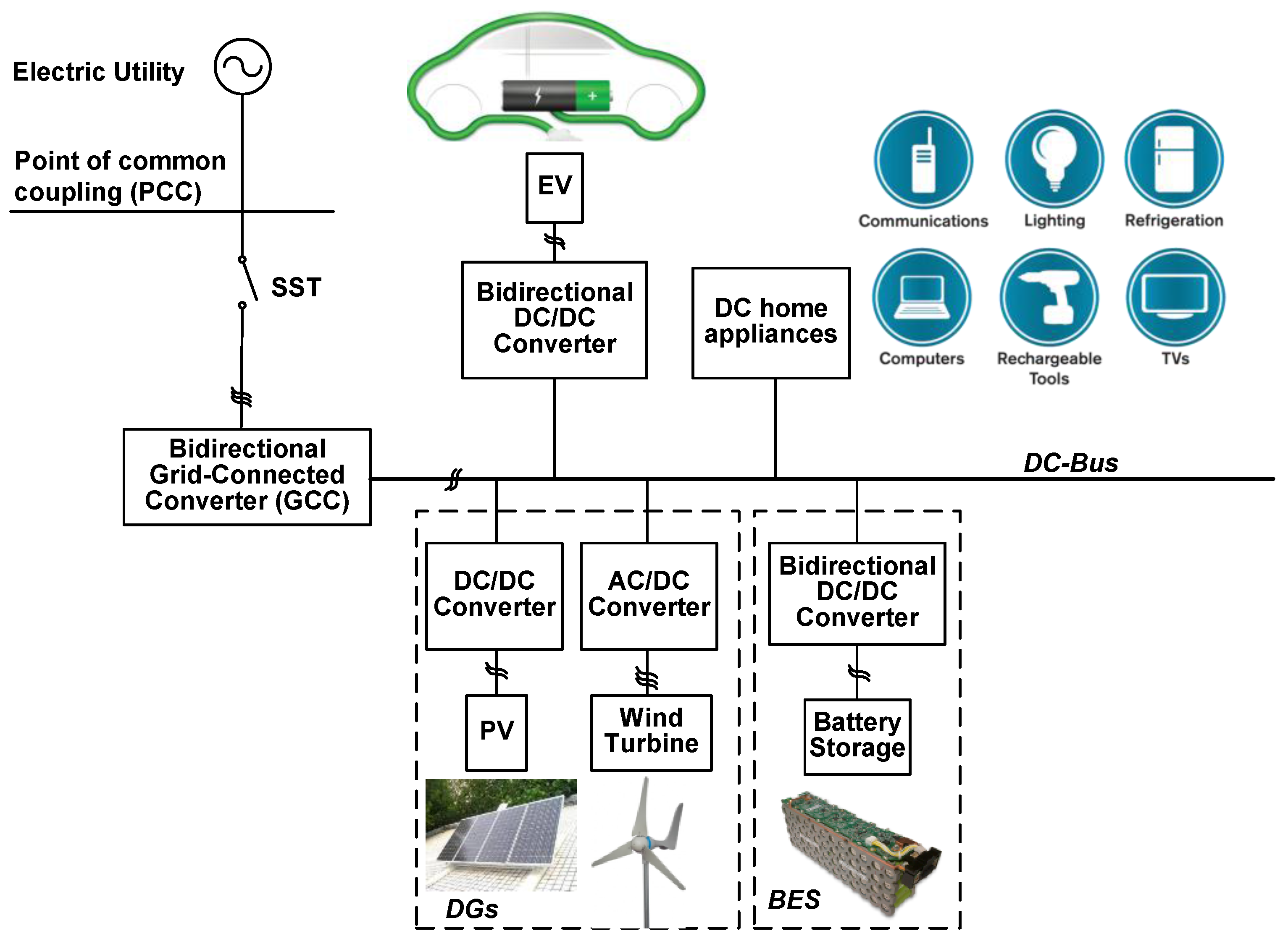
:1. Introduction
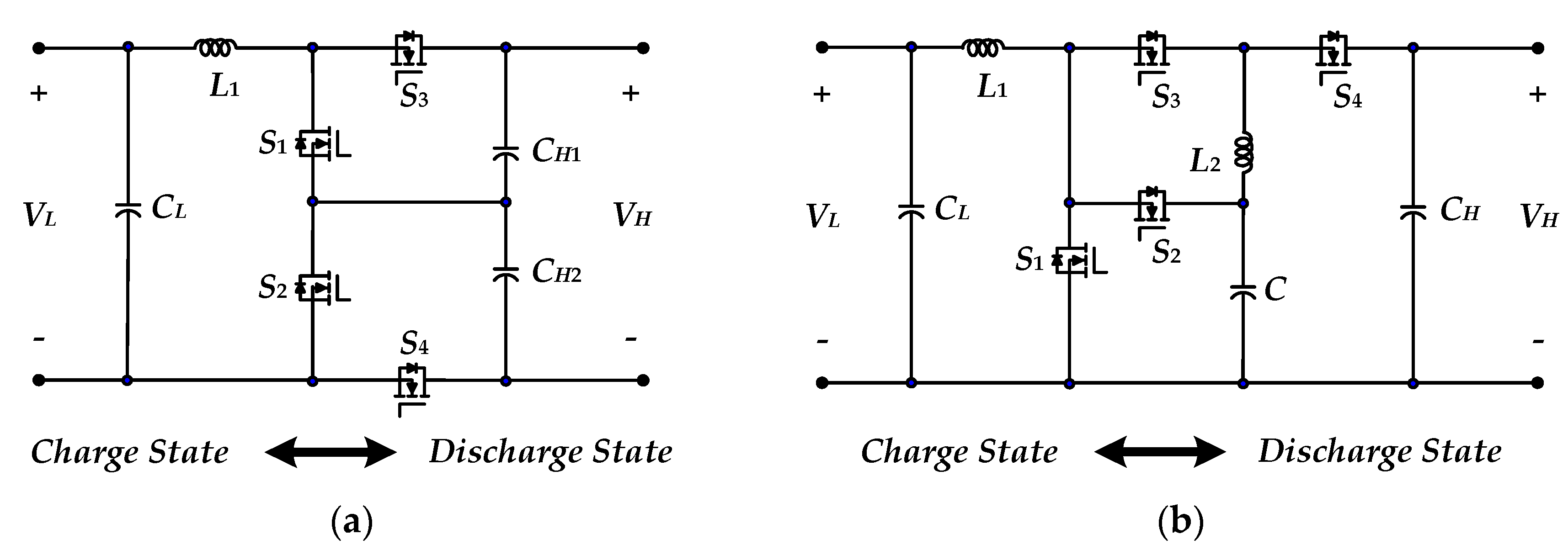
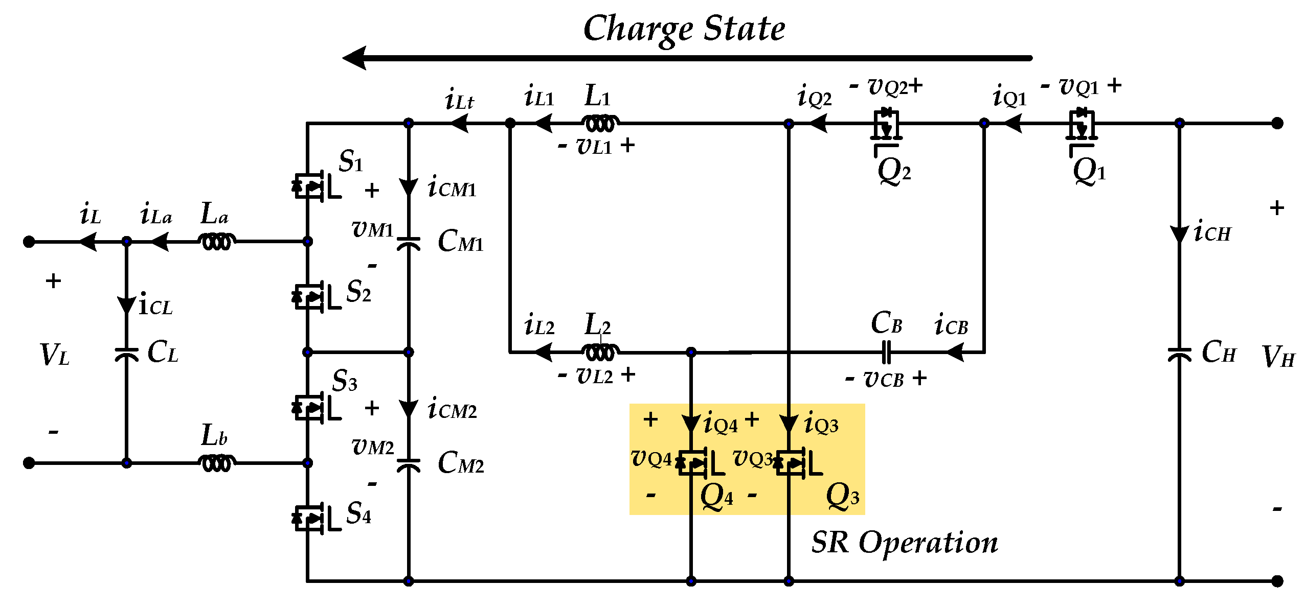
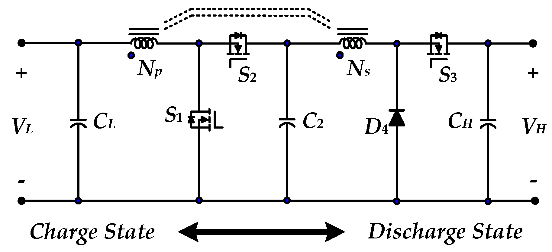
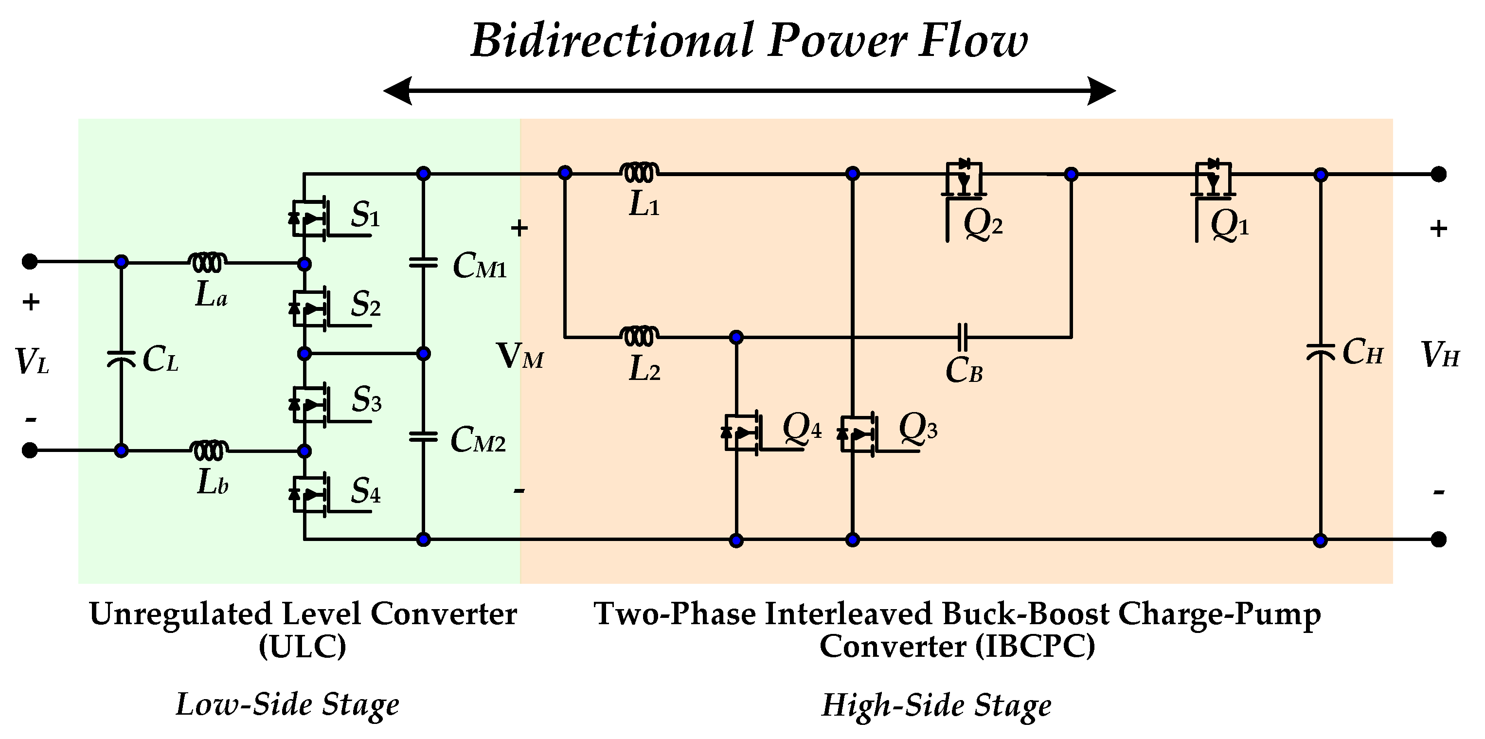
2. Proposed BDC Topology and Operation Principles
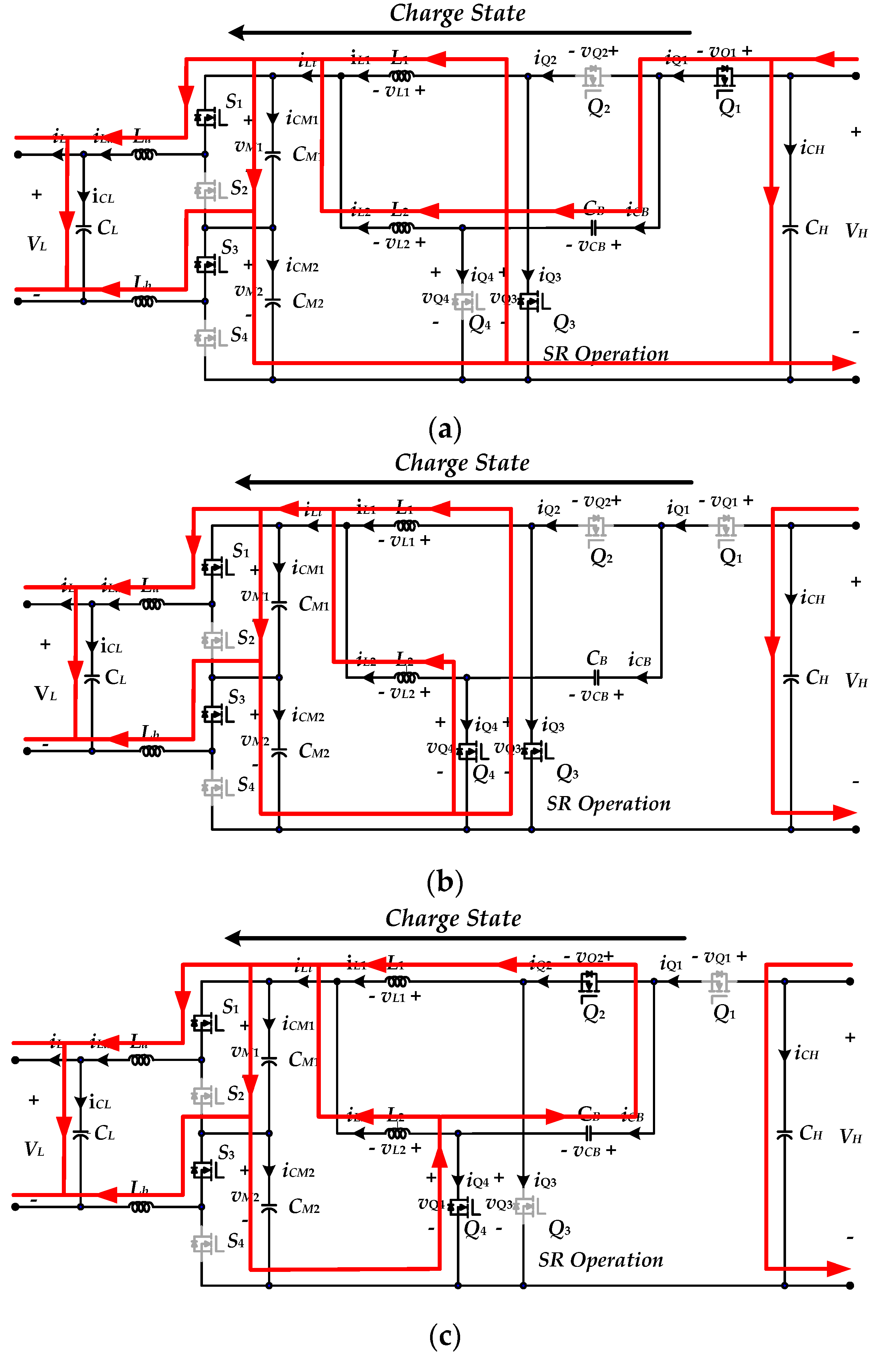
2.1. Charge State Operation
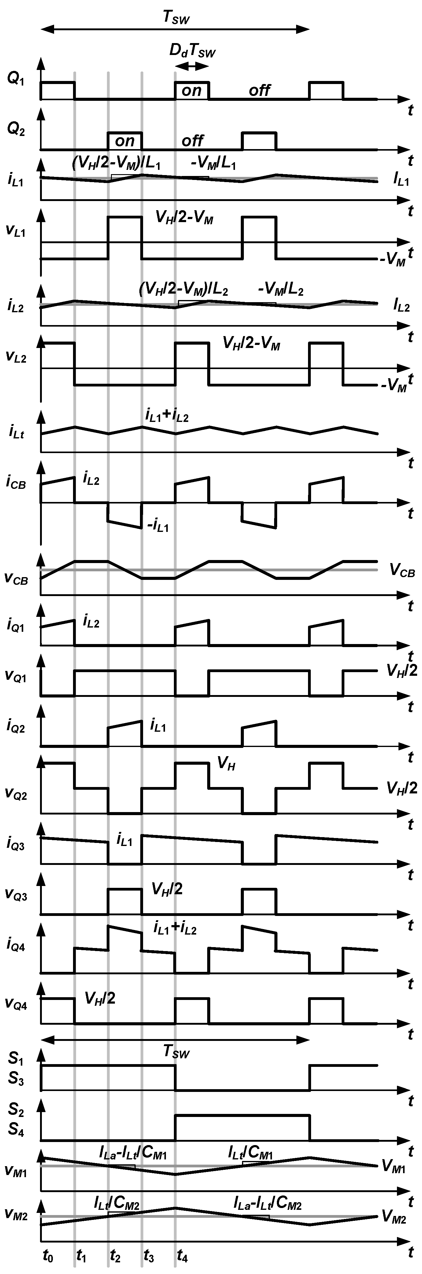
2.1.1. Mode 1 [t0 < t ≤ t1]
2.1.2. Mode 2 [t1 < t ≤ t2]
2.1.3. Mode 3 [t2 < t ≤ t3]
2.1.4. Mode 4 [t3 < t ≤ t4]
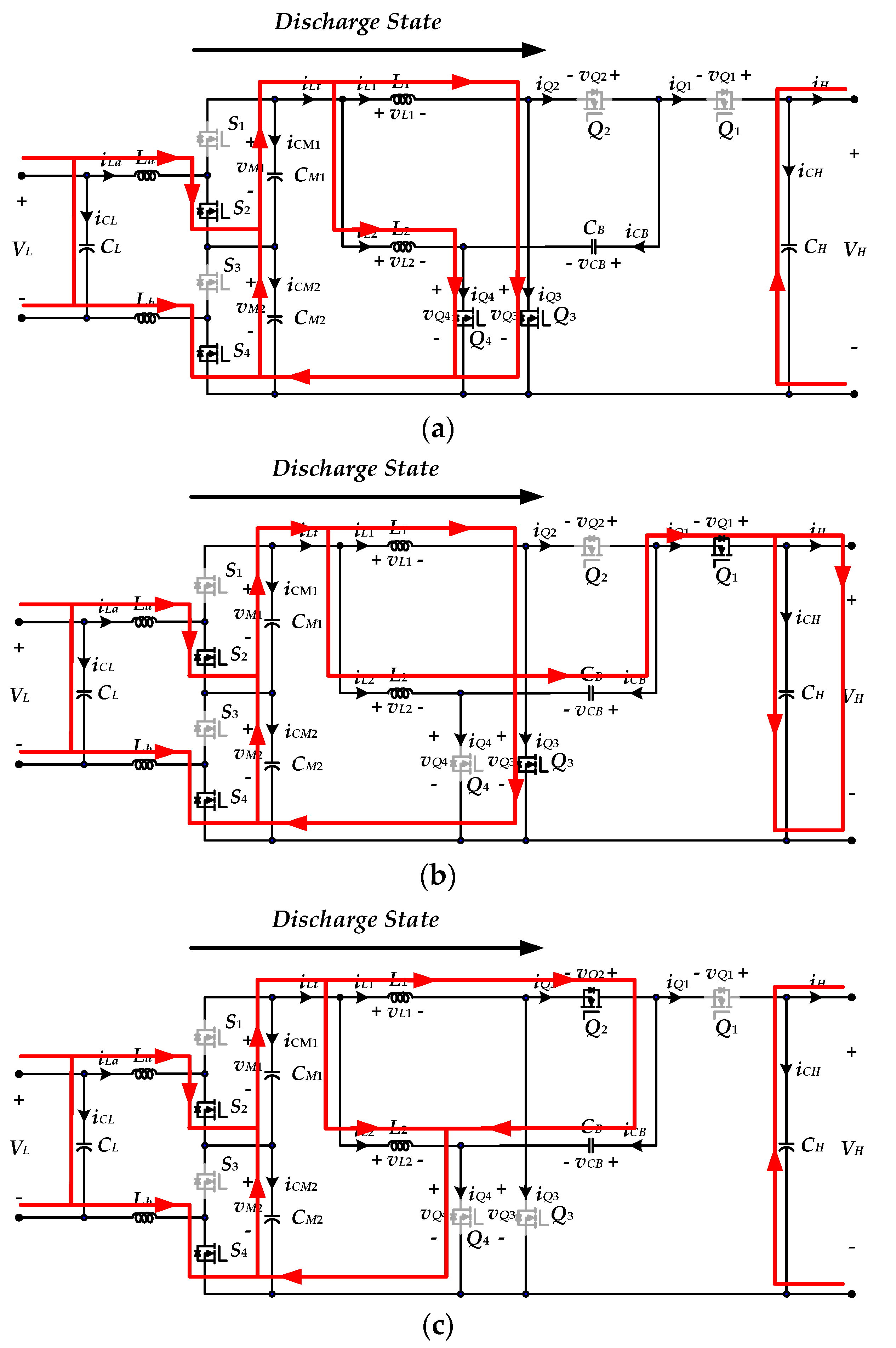
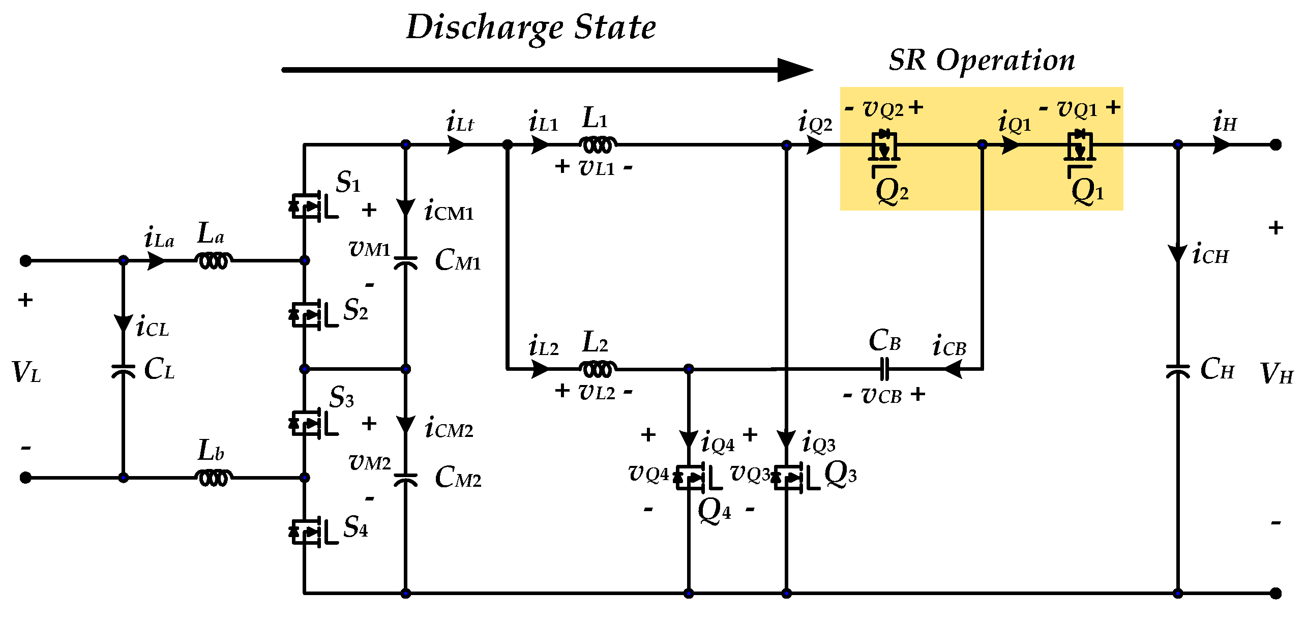
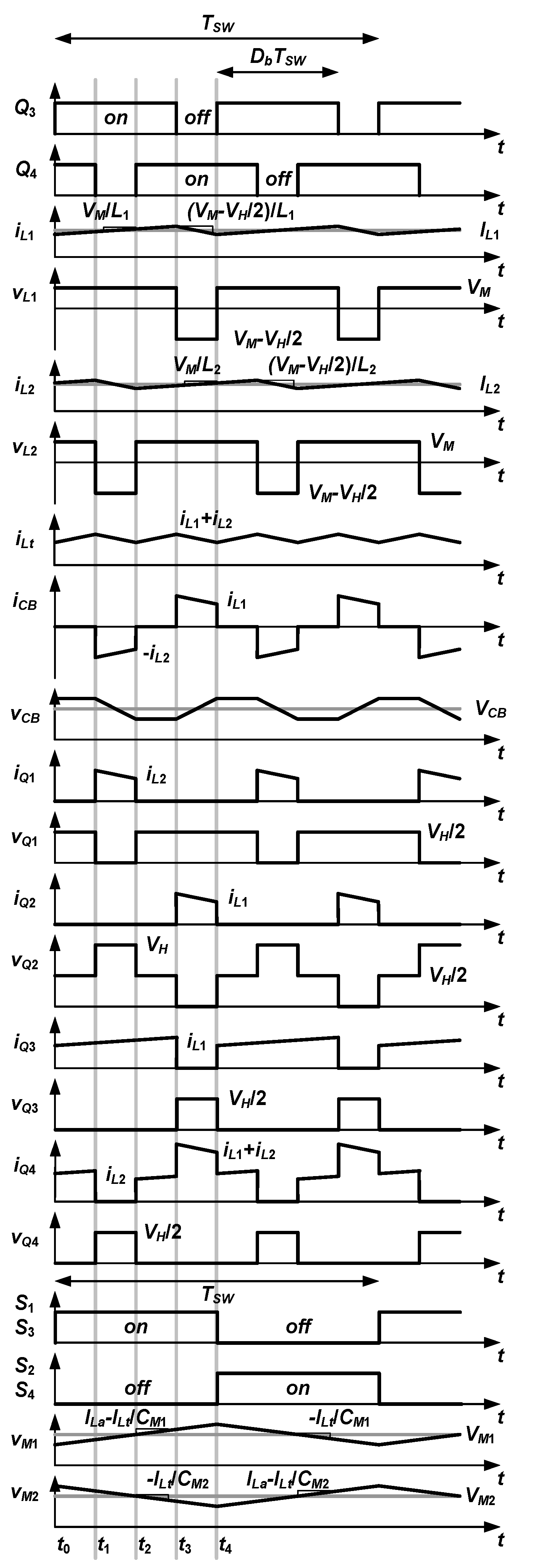
2.2. Discharge State Operation
2.2.1. Mode 1 [t0 < t ≤ t1]
2.2.2. Mode 2 [t1 < t ≤ t2]
2.2.3. Mode 3 [t2 < t ≤ t3]
2.2.4. Mode 4 [t3 < t ≤ t4]
3. Steady-State Analysis
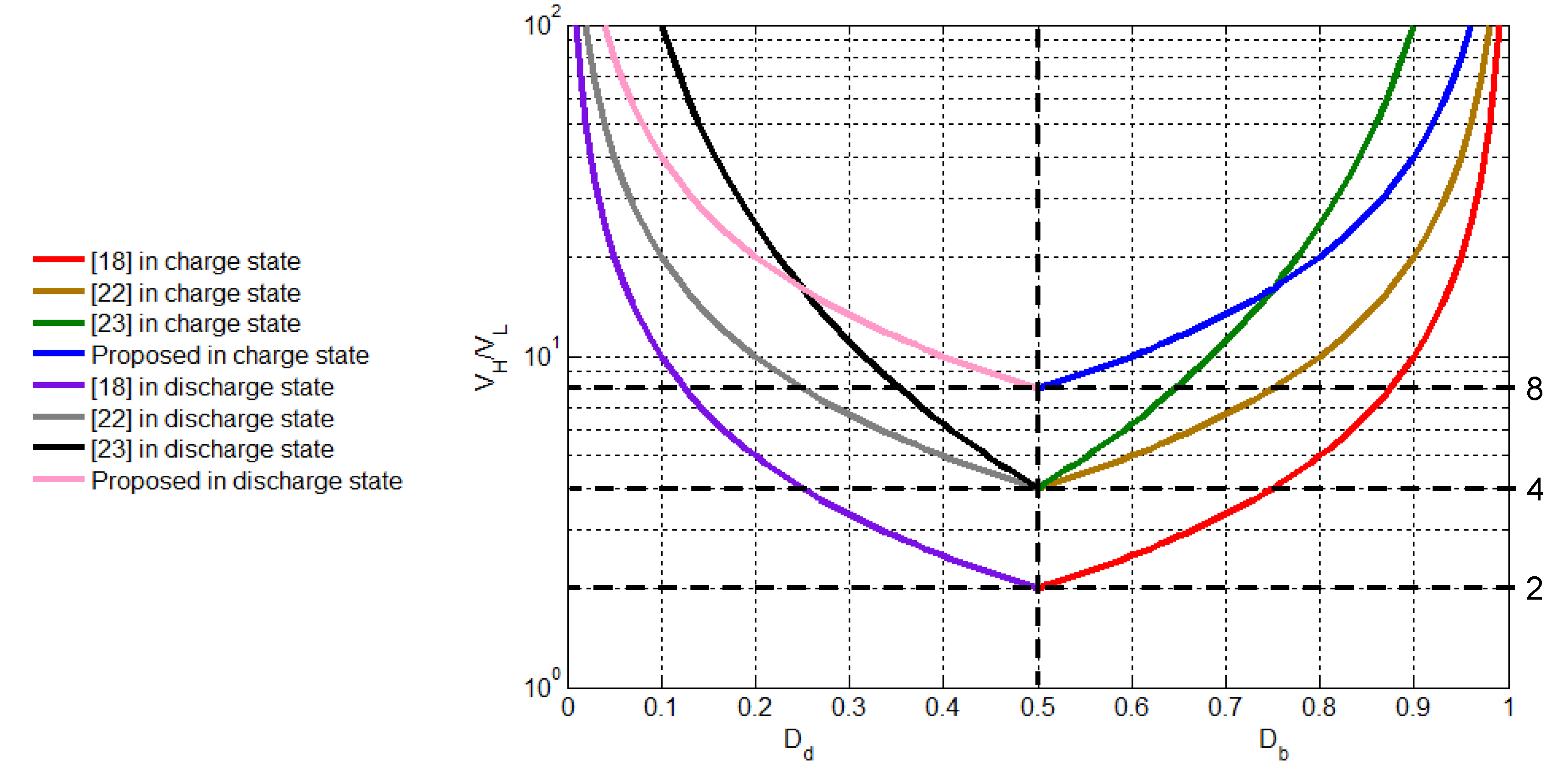
3.1. Voltage Conversion Ratio
3.2. Voltage Stress of the Switches
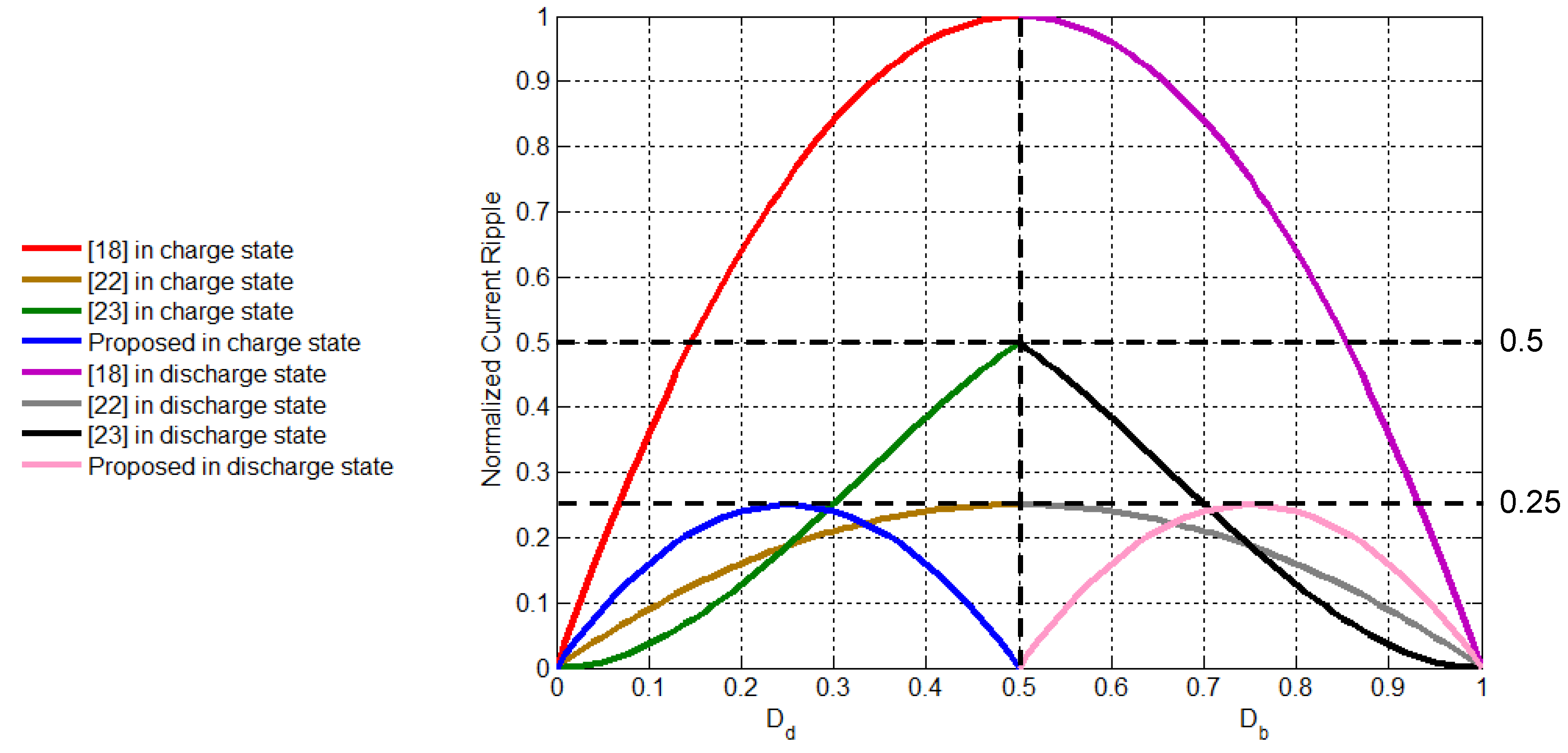
3.3. Inductor Current Ripple
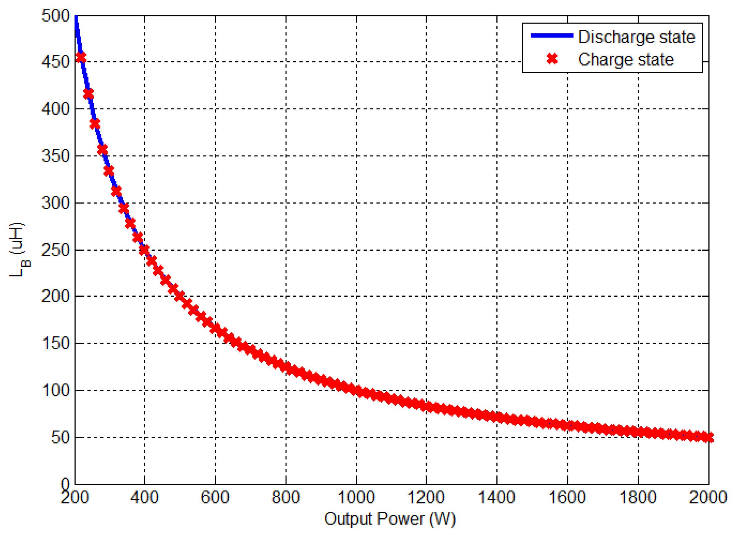
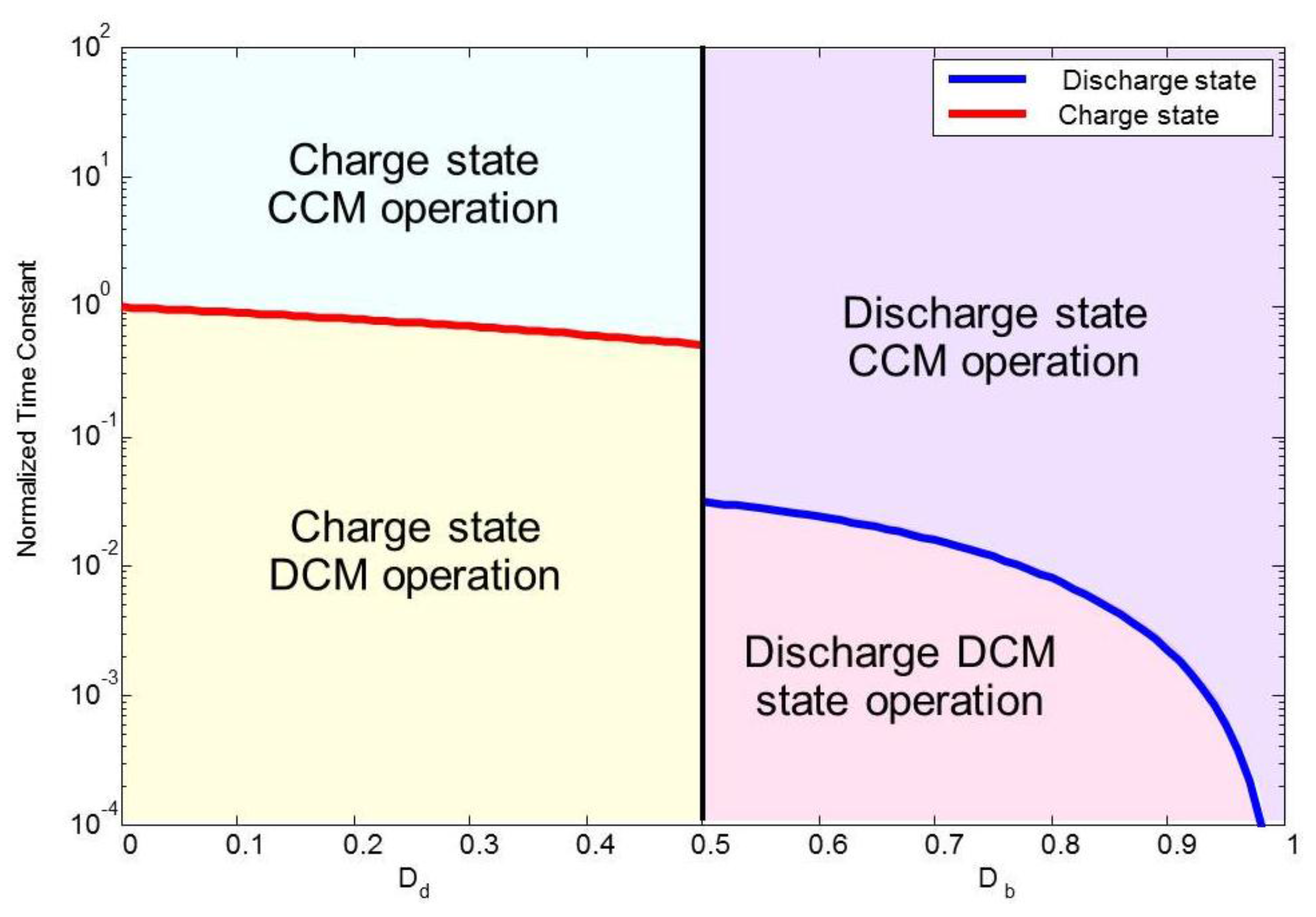
3.4. Boundary Conduction Mode
3.5. Selection Considerations of Charge-Pump Capacitor
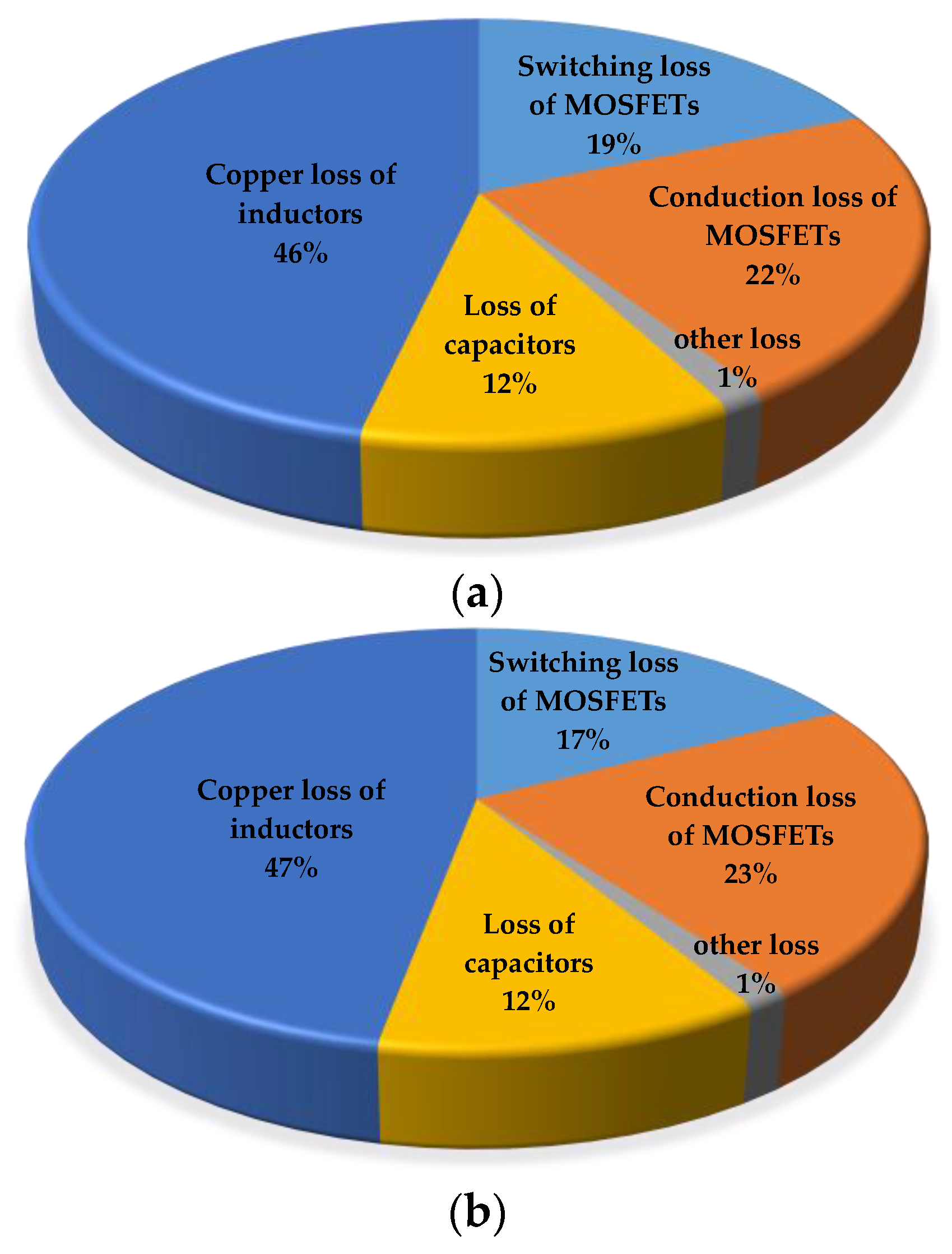
3.6. Summaries of Component Stress and Loss
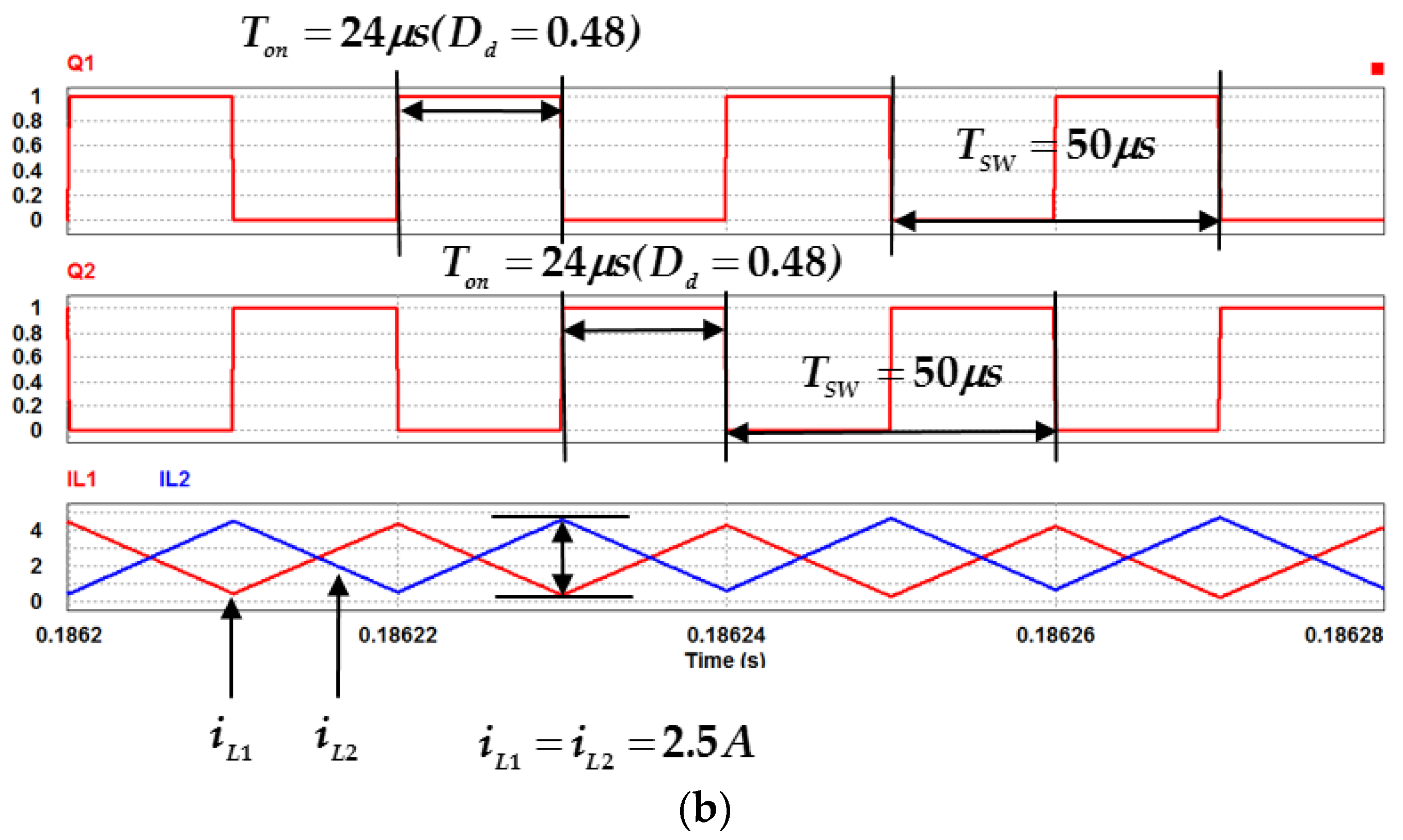
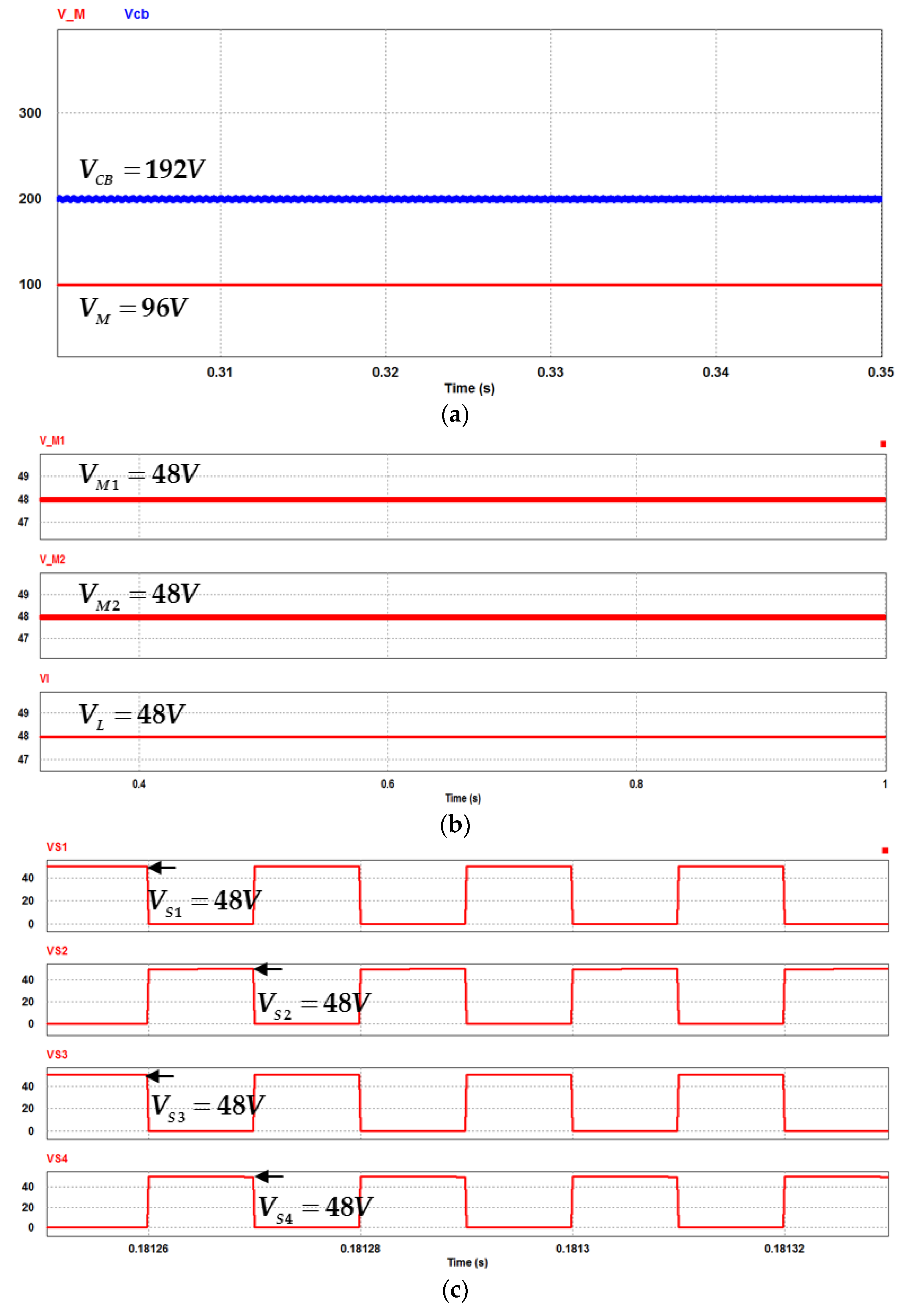
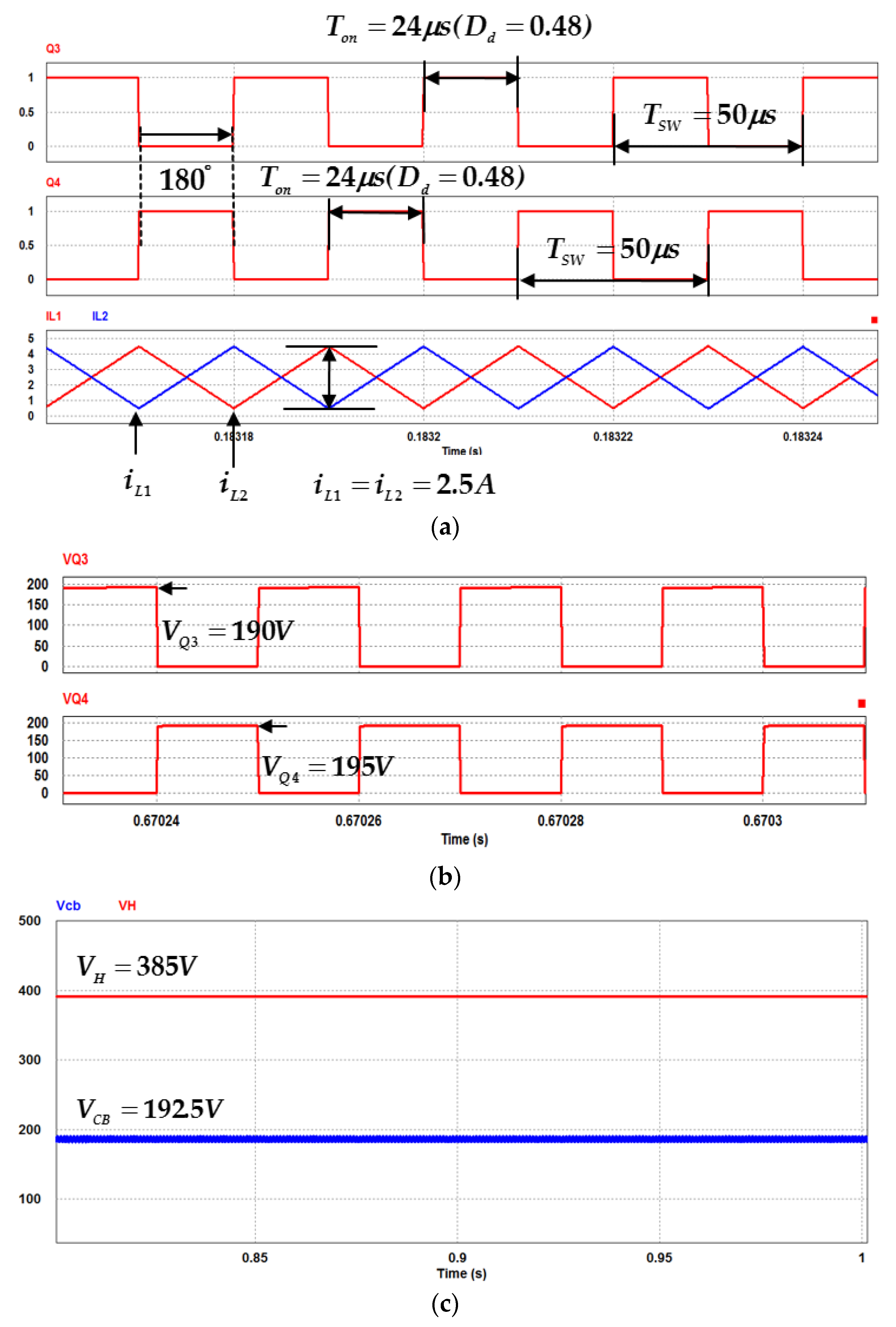
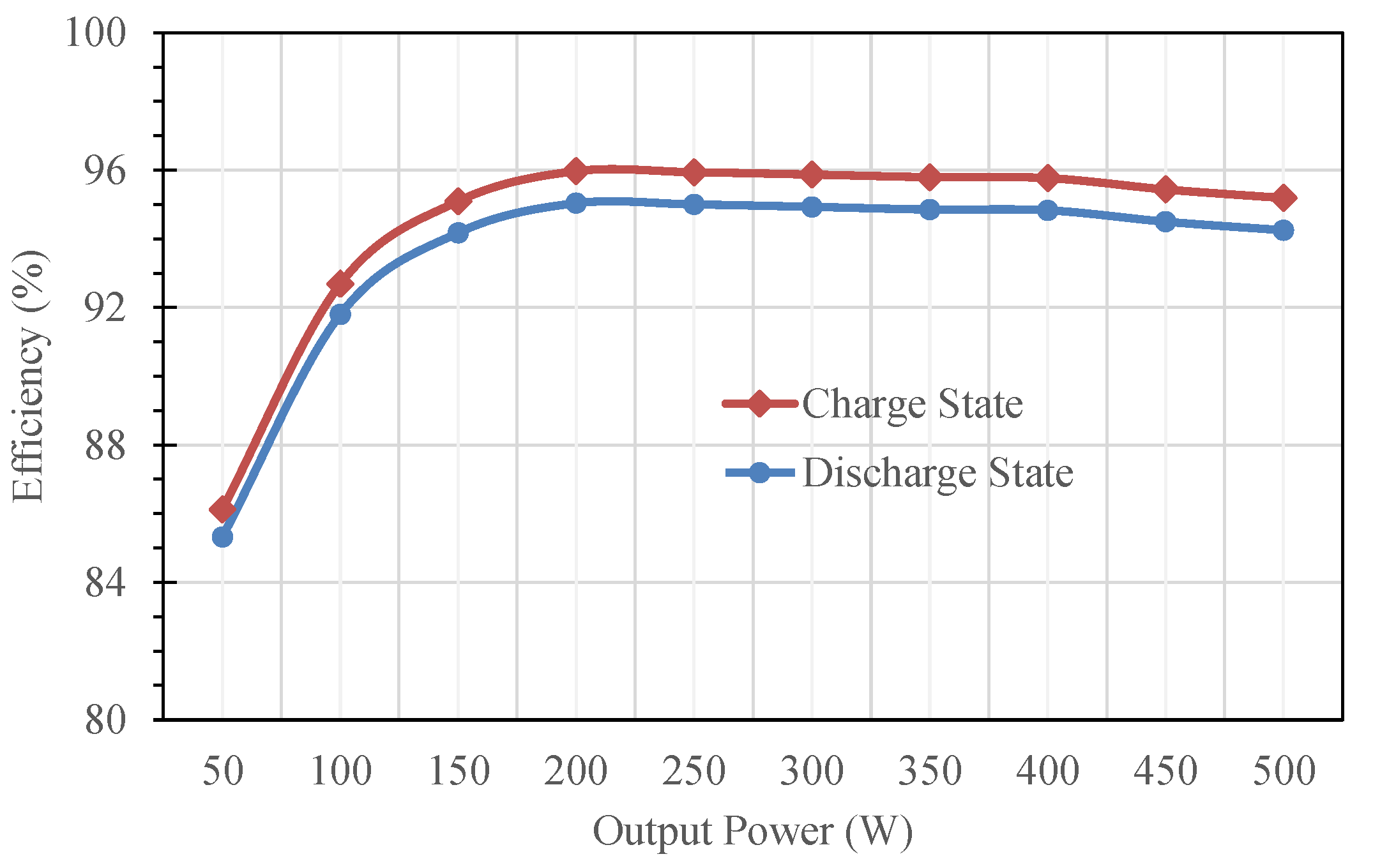
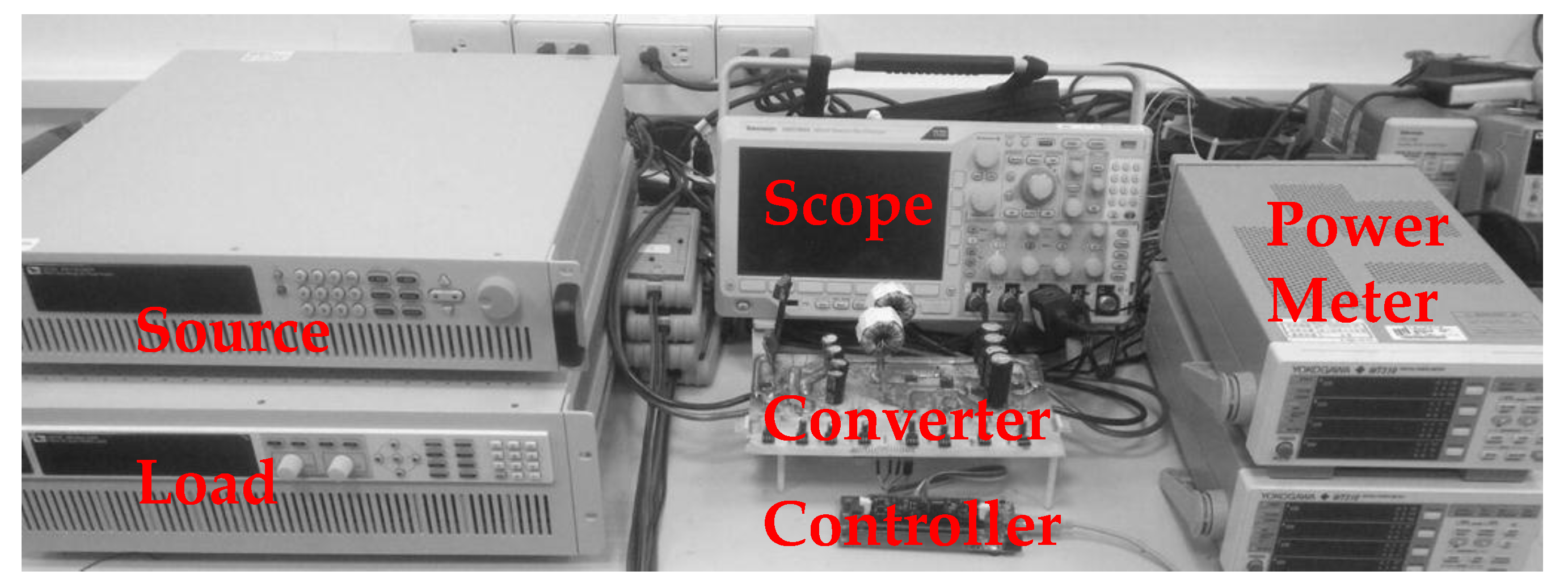
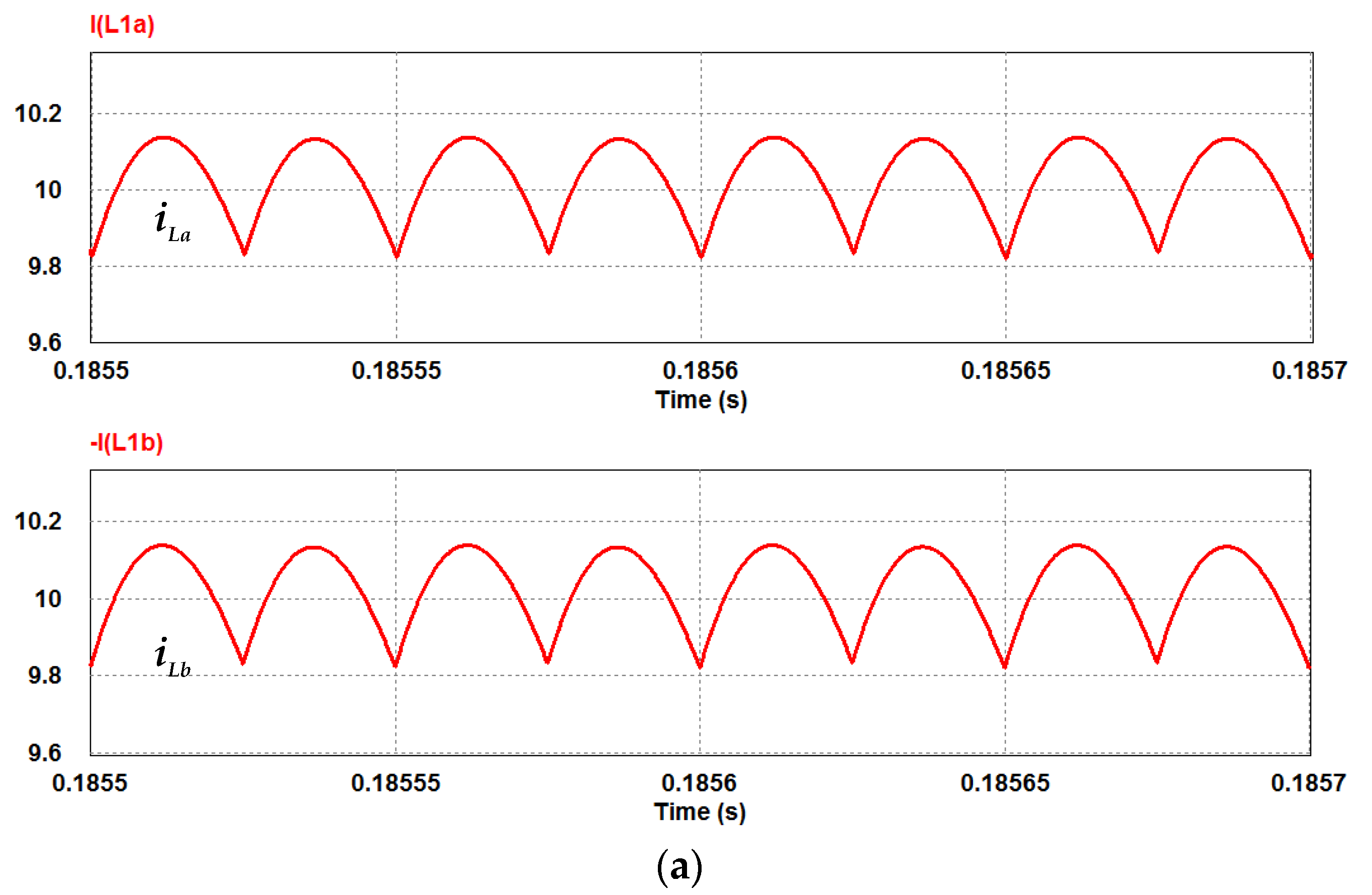
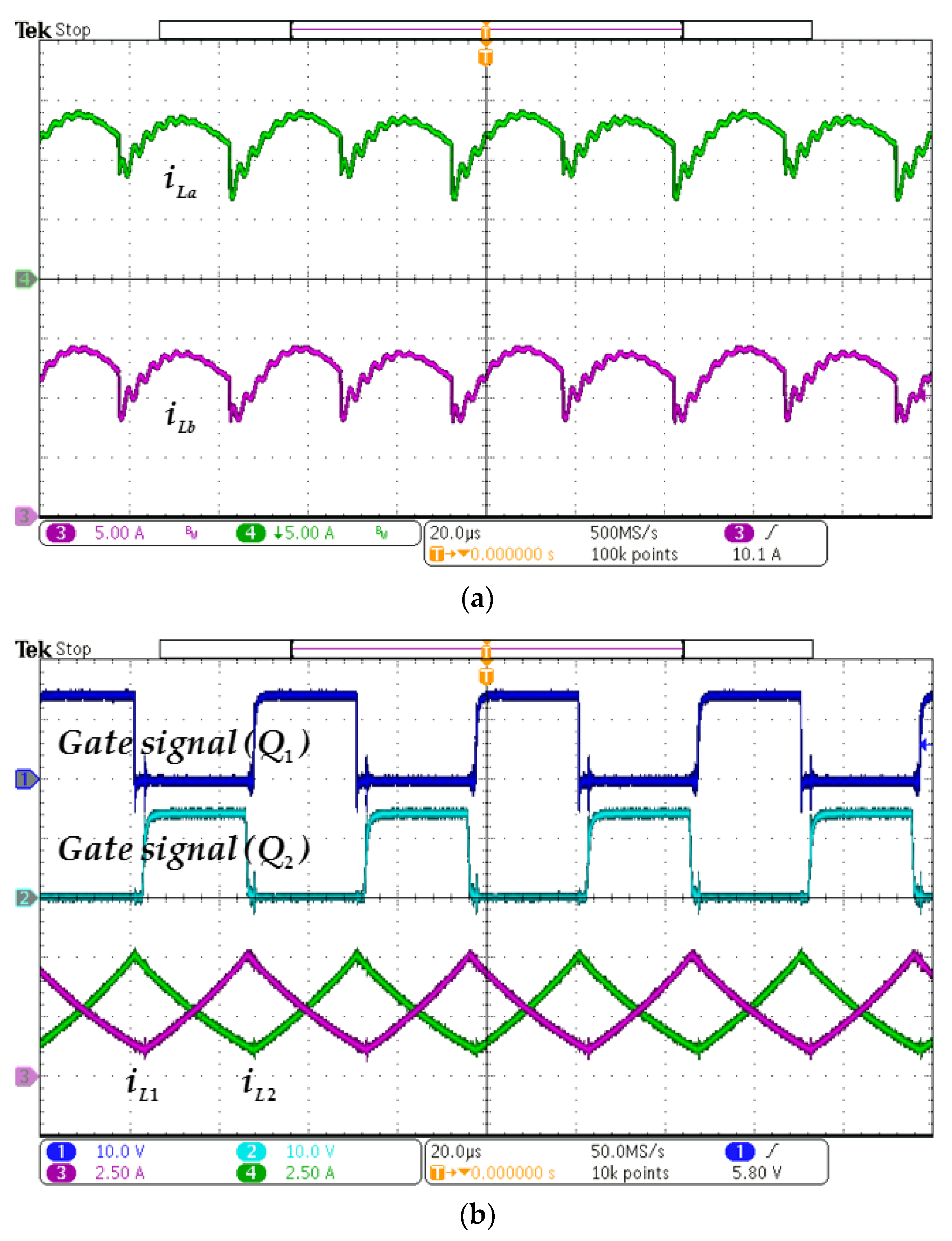
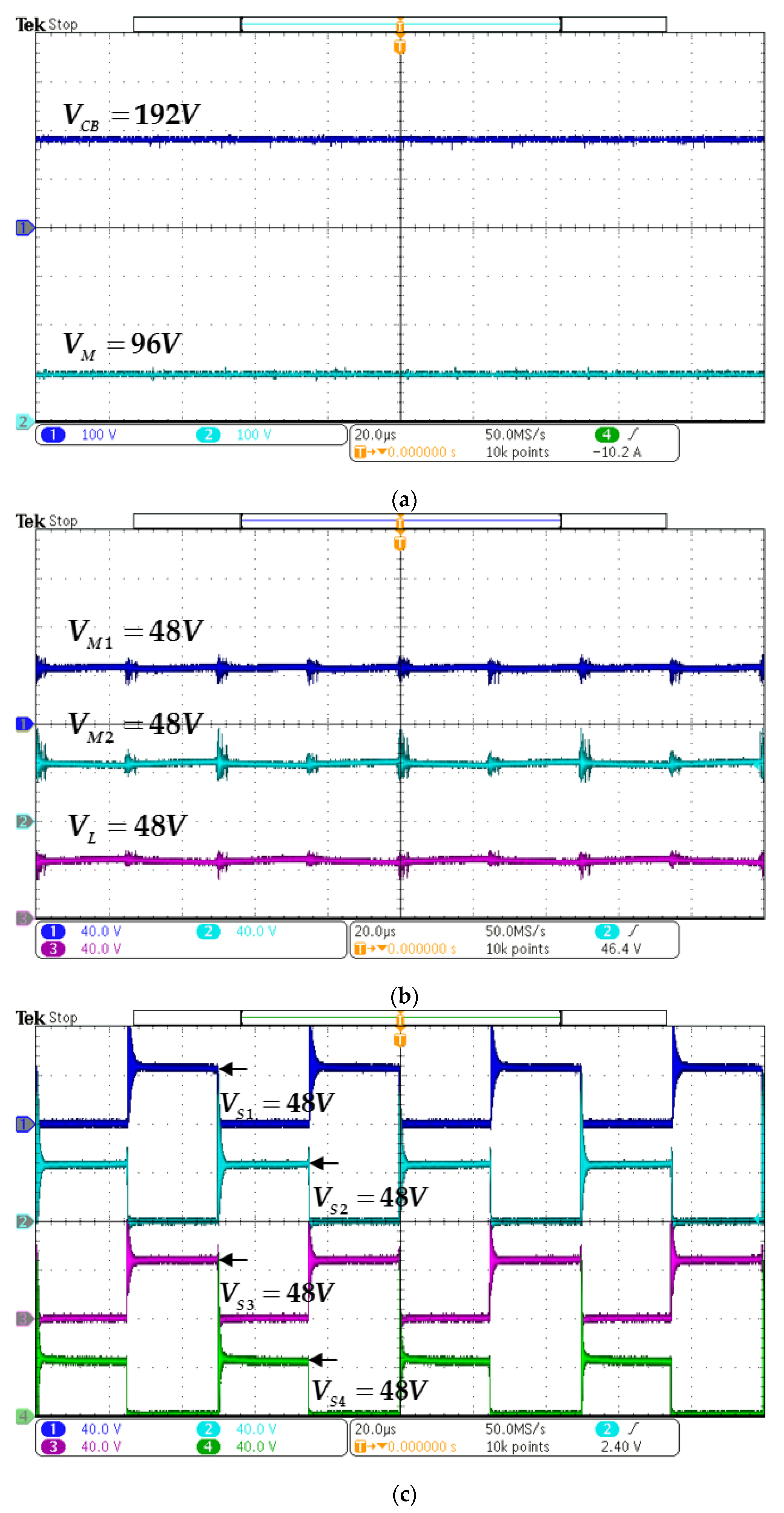
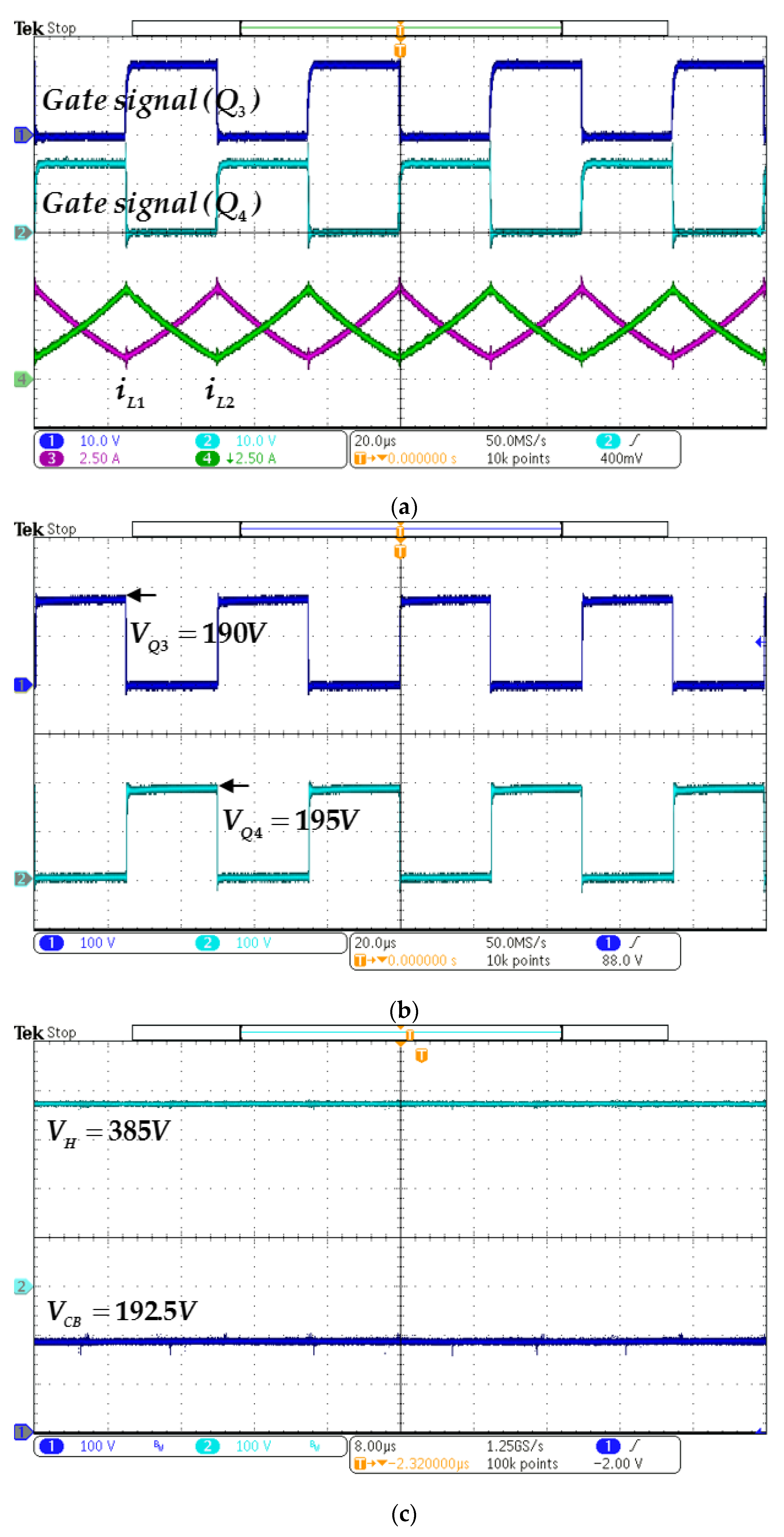
4. Simulation and Experimental Results
- (1)
- high-side voltage VH: 385 V;
- (2)
- low-side voltage VL: 48 V;
- (3)
- rated power Po: 500 W;
- (4)
- switching frequency fsw: 20 kHz;
- (5)
- capacitors CH = CL = 33 μF, CM1 = CM2 = 33 μF, CB = 10 μF; (ESR of CH, RCH = 0.064 Ω; ESR of CL, RCL = 0.062 Ω, ESR of CM1, RCM1 = 0.16 Ω; ESR of CM2, RCM2 = 0.16 Ω; ESR of CB, RCB = 0.062 Ω);
- (6)
- inductors L1 = L2 = Ls = 800 μH; La = Lb = 1.5 μH (IHLP-6767GZ-A1); (ESR of L1, RL1 = 0.18 Ω, ESR of L2, RL2 = 0.18 Ω, ESR of La, RLa = 13.6 mΩ; ESR of Lb, RLb = 13.6 mΩ);
- (7)
- power switches S1~S4: IXFH160N15T2, 150 V/160 A/RDS(on) = 9 mΩ, TO-247AC; Q1, Q3, Q4: FDA59N30, 300 V/59 A/RDS(on) = 56 mΩ, TO-247AC; Q2: W25NM60, 650 V/21 A/RDS(on) = 160 mΩ, TO-247AC.
5. Conclusions
Acknowledgments
Conflicts of Interest
References
- Lai, C.M.; Pan, C.T.; Cheng, M.C. High-efficiency modular high step-up interleaved boost converter for dc-microgrid applications. IEEE Trans. Ind. Appl. 2012, 48, 161–171. [Google Scholar] [CrossRef]
- Boroyevich, D.; Cvetkovic, I.; Burgos, R.; Dong, D. Intergrid: A future electronic energy network? IEEE J. Emerg. Sel. Top. Power Electron. 2013, 1, 127–138. [Google Scholar] [CrossRef]
- Yilmaz, M.; Krein, P.T. Review of the impact of vehicle-to-grid technologies on distribution systems and utility interfaces. IEEE Trans. Power Electron. 2013, 28, 5673–5689. [Google Scholar] [CrossRef]
- Lai, C.M.; Lin, Y.C.; Lee, D.S. Study and implementation of a two-phase interleaved bidirectional DC/DC converter for vehicle and dc-microgrid systems. Energies 2015, 8, 9969–9991. [Google Scholar] [CrossRef]
- Takeda, T.; Miyoshi, H.; Yukita, K.; Goto, Y.; Ichiyanagi, K. Power interchange by the DC bus in micro grids. In Proceedings of the IEEE International Conference on DC Microgrids, Atlanta, GA, USA, 7–10 June 2015; pp. 135–137.
- Wunder, B.; Ott, L.; Kaiser, J.; Han, Y.; Fersterra, F.; Marz, M. Overview of different topologies and control strategies for DC micro grids. In Proceedings of the IEEE International Conference on DC Microgrids, Atlanta, GA, USA, 7–10 June 2015; pp. 349–354.
- Hu, K.W.; Liaw, C.M. Incorporated operation control of DC microgrid and electric vehicle. IEEE Trans. Ind. Electron. 2016, 63, 202–215. [Google Scholar] [CrossRef]
- Du, Y.; Lukic, S.; Jacobson, B.; Huang, A. Review of high power isolated bi-directional DC-DC converters for PHEV/EV DC charging infrastructure. In Proceedings of the IEEE Energy Conversion Congress and Exposition, Phoenix, AZ, USA, 17–22 September 2011; pp. 553–560.
- Zhao, B.; Song, Q.; Liu, W.; Sun, Y. Overview of dual-active-bridge isolated bidirectional DC-DC converter for high-frequency-link power-conversion system. IEEE Trans. Power Electron. 2014, 29, 4091–4106. [Google Scholar] [CrossRef]
- Wai, R.J.; Liaw, J.J. High-efficiency-isolated single-input multiple-output bidirectional converter. IEEE Trans. Power Electron. 2015, 30, 4914–4930. [Google Scholar] [CrossRef]
- Du, Y.; Zhou, X.; Bai, S.; Lukic, S.; Huang, A. Review of non-isolated bi-directional DC-DC converters for plug-in hybrid electric vehicle charge station application at municipal parking decks. In Proceedings of the IEEE Applied Power Electronics Conference and Exposition, Palm Springs, CA, USA, 21–25 February 2010; pp. 1145–1151.
- Wai, R.J.; Duan, R.Y. High-efficiency bidirectional converter for power sources with great voltage diversity. IEEE Trans. Power Electron. 1997, 22, 1986–1996. [Google Scholar] [CrossRef]
- Wai, R.J.; Duan, R.Y.; Jheng, K.H. High-efficiency bidirectional DC-DC converter with high-voltage gain. IET Power Electron. 2012, 5, 173–184. [Google Scholar] [CrossRef]
- Yang, L.S.; Liang, T.J. Analysis and implementation of a novel bidirectional DC-DC converter. IEEE Trans. Ind. Electron. 2012, 59, 422–434. [Google Scholar] [CrossRef]
- Jiang, L.; Mi, C.; Li, S.; Zhang, M.; Zhang, X.; Yin, C. A novel soft-switching bidirectional DC-DC converter with coupled inductors. IEEE Trans. Ind. Appl. 2013, 49, 2730–2740. [Google Scholar] [CrossRef]
- Hsieh, Y.P.; Chen, J.F.; Yang, L.S.; Wu, C.Y.; Liu, W.S. High-conversion-ratio bidirectional DC-DC converter with coupled inductor. IEEE Trans. Ind. Electron. 2014, 61, 210–222. [Google Scholar] [CrossRef]
- Liang, T.J.; Liang, H.H.; Chen, S.M.; Chen, J.F.; Yang, L.S. Analysis, design, and implementation of a bidirectional double-boost DC-DC converter. IEEE Trans. Ind. Appl. 2014, 50, 3955–3962. [Google Scholar] [CrossRef]
- Chen, L.R.; Chu, N.Y.; Wang, C.S.; Liang, R.H. Design of a reflex-based bidirectional converter with the energy recovery function. IEEE Trans. Ind. Electron. 2008, 55, 3022–3029. [Google Scholar] [CrossRef]
- Han, D.; Noppakunkajorn, J.; Sarlioglu, B. Comprehensive efficiency, weight, and volume comparison of SiC- and Si-based bidirectional DC-DC converters for hybrid electric vehicles. IEEE Trans. Veh. Technol. 2014, 63, 3001–3010. [Google Scholar] [CrossRef]
- Jin, K.; Yang, M.; Ruan, X.; Xu, M. Three-level bidirectional converter for fuel-cell/battery hybrid power system. IEEE Trans. Ind. Electron. 2010, 57, 1976–1986. [Google Scholar] [CrossRef]
- Monge, S.B.; Alepuz, S.; Bordonau, J. A bidirectional multilevel boost-buck DC-DC converter. IEEE Trans. Power Electron. 2011, 26, 2172–2183. [Google Scholar] [CrossRef]
- Lin, C.C.; Yang, L.S.; Wu, G.W. Study of a non-isolated bidirectional DC-DC converter. IET Power Electron. 2013, 6, 30–37. [Google Scholar] [CrossRef]
- Ardi, H.; Ahrabi, R.R.; Ravadanegh, S.N. Non-isolated bidirectional DC-DC converter analysis and implementation. IET Power Electron. 2014, 7, 3033–3044. [Google Scholar] [CrossRef]
- Kabalo, M.; Paire, D.; Blunier, B.; Bouquain, D.; Simoes, M.G.; Miraoui, A. Experimental validation of high-voltage-ratio low input-current-ripple converters for hybrid fuel cell supercapacitor systems. IEEE Trans. Veh. Technol. 2012, 61, 3430–3440. [Google Scholar] [CrossRef]
- Lai, C.M.; Yang, M.J. A high-gain three-port power converter with fuel cell, battery sources and stacked output for hybrid electric vehicles and DC-microgrids. Energies 2016, 9, 180. [Google Scholar] [CrossRef]
- MOSFET Basics. Available online: https://www.fairchildsemi.com/application-notes/AN/AN-9010.pdf (accessed on 10 April 2016).
- Sattler, M.; Smetana, T.; Meyerhofer, T.; Kuhlkamp, L. 48 V minihybrid—A new solution for the minimale hybridization of vehicles. In Proceedings of the 22nd Aachen Colloquium Automobile and Engine Technology, Germany, 8 October 2013; pp. 995–1008.


| Items | Charge State | Discharge State |
|---|---|---|
| Voltage Stress of Q1, Q3, Q4 (vQ1, vQ3, vQ4) | ||
| Voltage Stress of Q2 (vQ2) | ||
| Voltage Stress of S1~S4 (vS1~vS4) | ||
| RMS Current Stress of Q1 (iQ1) | ||
| RMS Current Stress of Q2 (iQ2) | ||
| RMS Current Stress of Q3 (iQ3) | ||
| RMS Current Stress of Q4 (iQ4) | ||
| RMS Current Stress of S1~S4 (iS1~iS4) | ||
| RMS Current Stress of L1 (iL1) | ||
| RMS Current Stress of L2 (iL2) | ||
| RMS Current Stress of La (iLa) | ||
| RMS Current Stress of Lb (iLb) | ||
| RMS Current Stress of CB (iCB) | ||
| RMS Current Stress of CH (iCH) | ||
| RMS Current Stress of CL (iCL) | ||
| RMS Current Stress of CM1, CM2 (iCM1, iCM2) |
| Items | Equations |
|---|---|
| Conduction loss of Q1~Q4 | ; ; ; |
| Conduction loss of S1~S4 | ; ; ; |
| Switching loss of Q1 | ; |
| Switching loss of Q2 | ; |
| Switching loss of Q3 | ; |
| Switching loss of Q4 | ; |
| Switching loss of S1 | ; |
| Switching loss of S2 | ; |
| Switching loss of S3 | ; |
| Switching loss of S4 | ; |
| Conduction loss of L1~L2 | ; |
| Conduction loss of La~Lb | ; |
| Conduction loss of CB, CH, CL | ; ; |
| Conduction loss of CM1~ CM2 | ; |
| Gate driving loss of Q1~Q4 | |
| Gate driving loss of S1~S4 |
| Items | Charge State | Discharge State |
|---|---|---|
| Calculated Results | Calculated Results | |
| Conduction loss of Q1 | 0.62 W | 0.62 W |
| Conduction loss of Q2 | 1.58 W | 1.58 W |
| Conduction loss of Q3 | 0.67 W | 0.67 W |
| Conduction loss of Q4 | 1.29 W | 1.29 W |
| Conduction loss of S1 | 0.58 W | 0.58 W |
| Conduction loss of S2 | 0.58 W | 0.58 W |
| Conduction loss of S3 | 0.58 W | 0.58 W |
| Conduction loss of S4 | 0.58 W | 0.58 W |
| Switching loss of Q1 (turn on/off transition) | on: 0.09 W; off: 0.52 W | on: 0.10 W; off: 0.72 W |
| Switching loss of Q2 (turn on/off transition) | on: 0.19 W; off: 1.01 W | on: 0.17 W; off: 0.87 W |
| Switching loss of Q3 (turn on/off transition) | on: 0.09 W; off: 0.62 W | on: 0.09 W; off: 0.52 W |
| Switching loss of Q4 (turn on/off transition) | on: 0.10 W; off: 0.69 W | on: 0.09 W; off: 0.54 W |
| Switching loss of S1 (turn on/off transition) | on: 0.07 W; off: 0.44 W | on: 0.05 W; off: 0.55 W |
| Switching loss of S2 (turn on/off transition) | on: 0.05 W; off: 0.60 W | on: 0.06 W; off: 0.35 W |
| Switching loss of S3 (turn on/off transition) | on: 0.05 W; off: 0.47 W | on: 0.05 W; off: 0.29 W |
| Switching loss of S4 (turn on/off transition) | on: 0.06 W; off: 0.34 W | on: 0.05 W; off: 0.46 W |
| Conduction loss of L1 | 4.94 W | 4.94 W |
| Conduction loss of L2 | 4.94 W | 4.94 W |
| Conduction loss of La | 1.80 W | 1.80 W |
| Conduction loss of Lb | 1.80 W | 1.80 W |
| Conduction loss of CB | 1.61 W | 1.61 W |
| Conduction loss of CH | 1.67 W | 1.67 W |
| Conduction loss of CL | 0.02 W | 0.02 W |
| Conduction loss of CM1 | 0.01 W | 0.01 W |
| Conduction loss of CM2 | 0.01 W | 0.01 W |
| Gate driving loss of Q1~Q4 | 0.02 W | 0.02 W |
| Gate driving loss of S1~S4 | 0.08 W | 0.08 W |
| Total losses | 28.5 W | 28.64 W |
| % in rated load condition | 5.70% | 5.73% |
| Calculated Efficiency | 94.30% | 94.27% |
| Measured Efficiency | 94.29% | 94.25% |
| Items | Topology | |||
|---|---|---|---|---|
| This Work | [17] | [22] | [23] | |
| Switching control structure | two-phase | single-phase | single-phase | single-phase |
| Output ripple | Low | High | Medium | Medium |
| Step-up conversion ratio | 4/(1 − Db) | n/(1 − Db) | 2/(1 − Db) | 1/(1 − Db)2 |
| Step-down conversion ratio | Dd/4 | Dd/(1 + n − nDd) | Dd/2 | (Dd)2 |
| High-side voltage | 385 V | 400 V | 200 V | 62.5 V |
| Low-side voltage | 48 V | 48 V | 24 V | 10 V |
| Realized prototype power rating | 500 W | 200 W | 200 W | 100 W |
| Number of main switches | 8 | 4 | 4 | 4 |
| Number of storage components | 7 | 5 | 5 | 5 |
| Maximum efficiency (charge state) | 96% | 91.6% | 94.8% | 91.5% |
| Maximum efficiency (discharge state) | 95% | 94.3% | 94.1% | 92.5% |
© 2016 by the author; licensee MDPI, Basel, Switzerland. This article is an open access article distributed under the terms and conditions of the Creative Commons Attribution (CC-BY) license (http://creativecommons.org/licenses/by/4.0/).
Share and Cite
Lai, C.-M. Development of a Novel Bidirectional DC/DC Converter Topology with High Voltage Conversion Ratio for Electric Vehicles and DC-Microgrids. Energies 2016, 9, 410. https://doi.org/10.3390/en9060410
Lai C-M. Development of a Novel Bidirectional DC/DC Converter Topology with High Voltage Conversion Ratio for Electric Vehicles and DC-Microgrids. Energies. 2016; 9(6):410. https://doi.org/10.3390/en9060410
Chicago/Turabian StyleLai, Ching-Ming. 2016. "Development of a Novel Bidirectional DC/DC Converter Topology with High Voltage Conversion Ratio for Electric Vehicles and DC-Microgrids" Energies 9, no. 6: 410. https://doi.org/10.3390/en9060410
APA StyleLai, C.-M. (2016). Development of a Novel Bidirectional DC/DC Converter Topology with High Voltage Conversion Ratio for Electric Vehicles and DC-Microgrids. Energies, 9(6), 410. https://doi.org/10.3390/en9060410