
How the Chlorine Treatment and the Stoichiometry Influences the Grain Boundary Passivation in Polycrystalline CdTe Thin Films

Abstract
:
1. Introduction
2. Experimental
2.1. The Solar Cell
2.2. Characterization
3. Results and Discussion
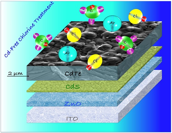
3.1. The Chlorine Treatment
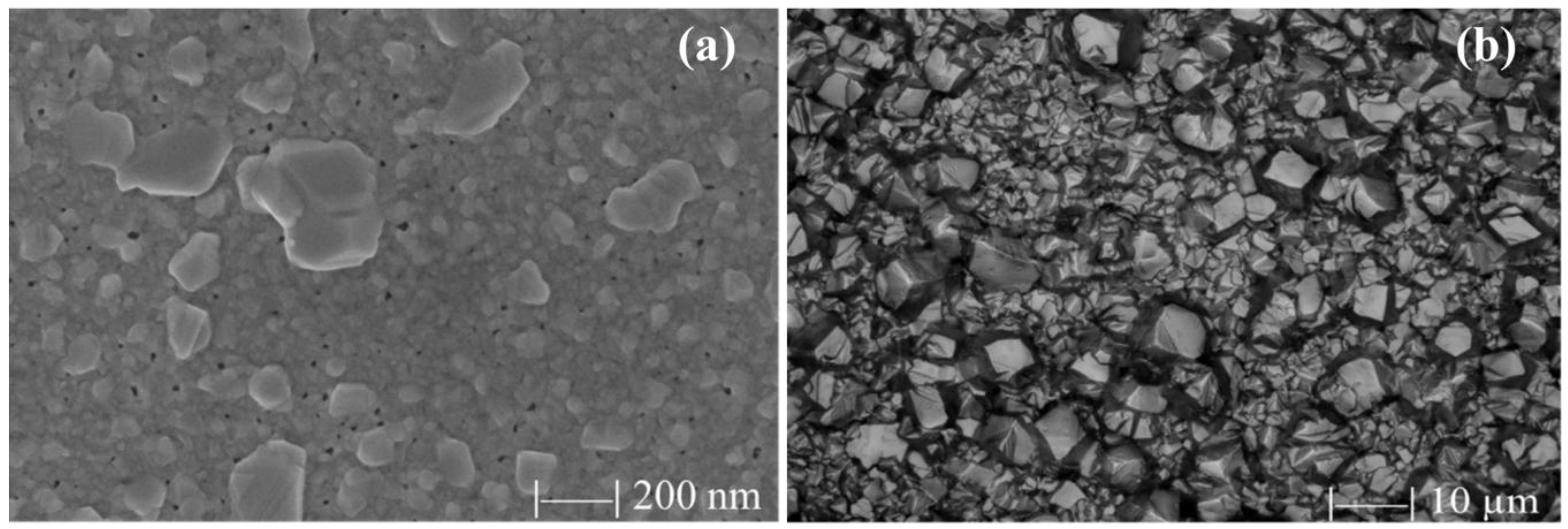
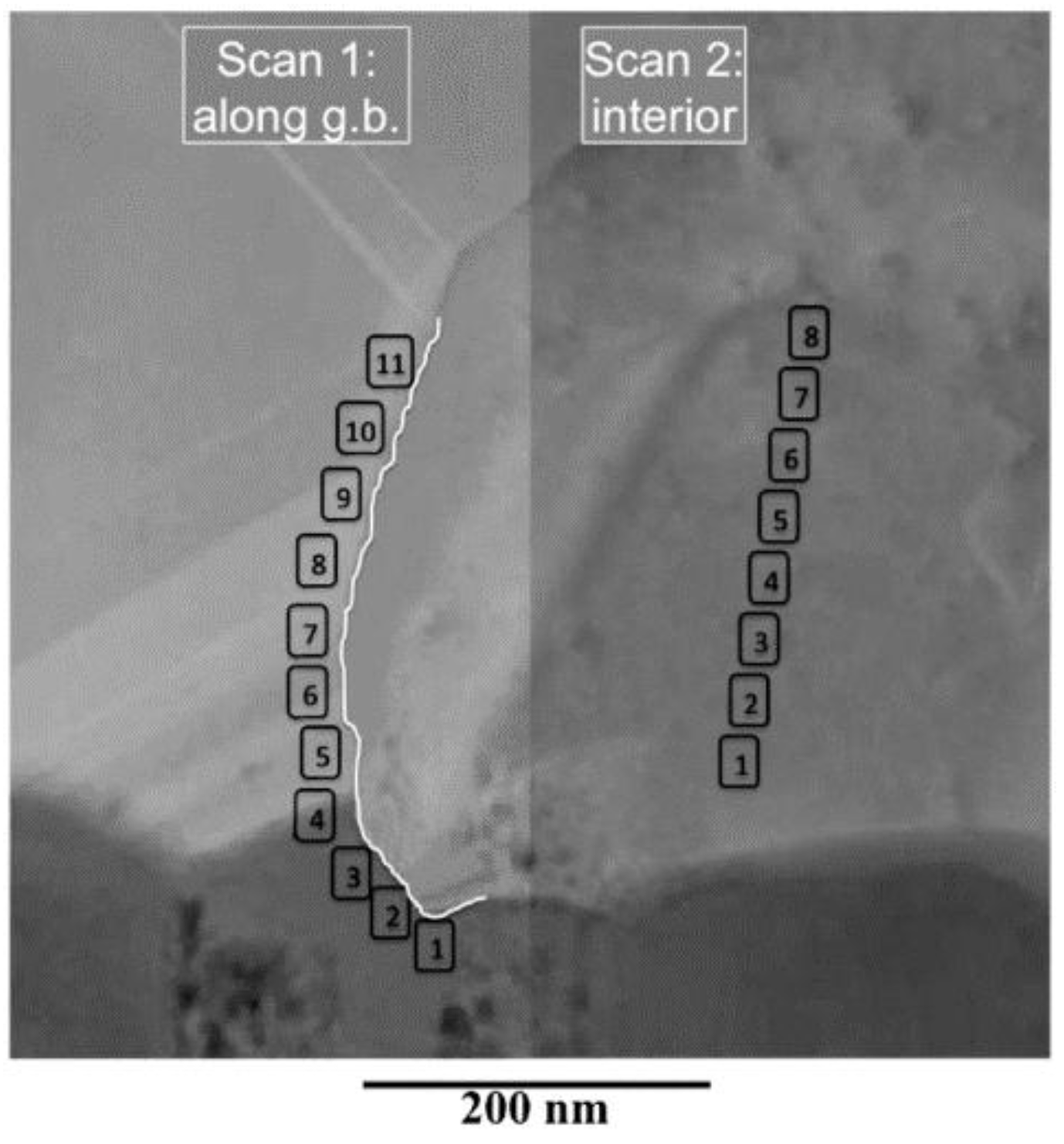
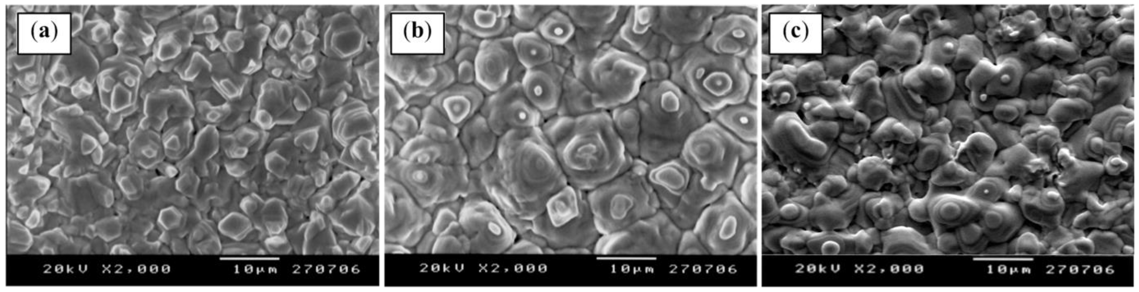
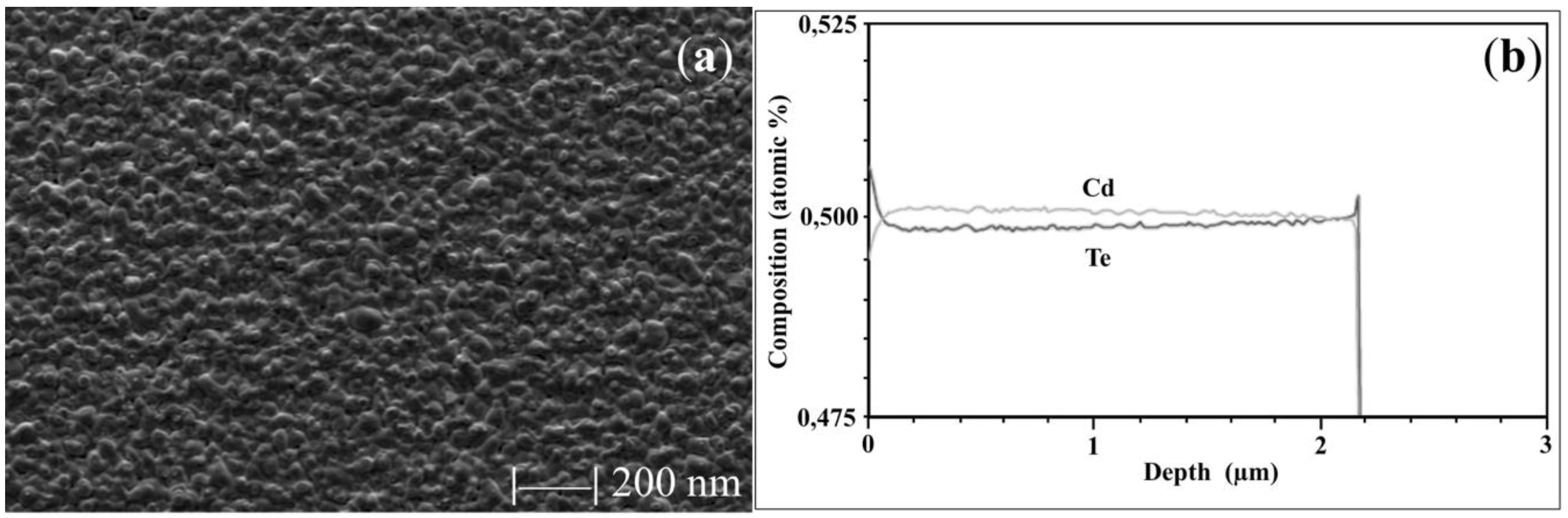
3.2. Pinholes and Grain Boundaries Passivation
4. Conclusions
Author Contributions
Conflicts of Interest
References
- Bonnet, D.; Rabenhorst, H. New results on the development of thin film p-CdTe/n-CdS hetero-junction solar cells. In Proceedings of the 9th Photovoltaic Specialists Conference, New York, NY, USA, 1972; pp. 129–131.
- Ferekides, C.; Britt, J.; Ma, Y.; Killian, L. High efficiency CdTe solar cells by close spaced sublimation. In Proceedings of the 20th IEEE Photovoltaic Specialists Conference, Louisville, KY, USA, 10–14 May 1993; pp. 389–393.
- Chu, T.L.; Chu, S.S.; Ferekides, C.; Wu, C.Q.; Britt, J.; Wang, C. 13.4% efficient thin-film CdS/CdTe solar cells. J. Appl. Phys. 1991, 70, 7608–7612. [Google Scholar] [CrossRef]
- Hanket, G.M.; McCandless, B.E.; Buchanan, W.A.; Fields, S.; Birkmire, R.W. Design of a vapor transport deposition process for thin film materials. J. Vac. Sci.Tech. A 2006, 24, 1695–1701. [Google Scholar] [CrossRef]
- Meyers, P.V.; Kee, R.J.; Raja, L.; Wolden, C.A.; Aire, M. Atmospheric pressure chemical vapor deposition of CdTe-reactor design considerations. In Proceedings of the 15th AIP National Center for Photovoltaics (NCPV) Program Review Meeting, Denver, CO, USA, 9–11 September 1998; pp. 218–223.
- Romeo, A.; Buecheler, S.; Giarola, M.; Mariotto, G.; Tiwari, A.N.; Romeo, N.; Bosio, A.; Mazzamuto, S. Study of CSS- and HVE-CdTe by different recrystallization processes. Thin Solid Films 2009, 517, 2132–2135. [Google Scholar] [CrossRef]
- Shao, M.; Fischer, A.; Grecu, D.; Jayamaha, U.; Bykov, E.; Contreras-Puente, G.; Bohn, R.G.; Compaan, A.D. Radio-frequency-magnetron-sputtered CdS/CdTe solar cells on soda-lime glass. Appl. Phys. Lett. 1996, 69, 3045–3047. [Google Scholar] [CrossRef]
- Ma, Y.Y.; Fahrenbruch, A.L.; Bube, R.H. Photovoltaic properties of n-cadmium sulfide/p-cadmium telluride hetero-junctions prepared by spray pyrolysis. Appl. Phys. Lett. 1977, 30, 423–424. [Google Scholar] [CrossRef]
- Panicker, M.P.R.; Knaster, M.; Kröger, F.A. Cathodic deposition of CdTe from aqueous electrolytes. J. Electrochem. Soc. 1978, 125, 566–572. [Google Scholar] [CrossRef]
- Ferekides, C.; Marinskiy, D.; Morel, D.L. CdS: Characterization and recent advances in CdTe solar cell performance. In Proceedings of the 26th IEEE Photovoltaic Specialists Conference, Anaheim, CA, USA, 29 September–3 October 1997; pp. 339–342.
- Mazzamuto, S.; Vaillant, L.; Bosio, A.; Romeo, N.; Armani, N.; Salviati, G. A study of the CdTe treatment with a Freon gas such as CHF2Cl. Thin Solid Films 2008, 516, 7079–7083. [Google Scholar] [CrossRef]
- Dobson, K.D.; Visoly-Fisher, I.; Hodes, G.; Cahen, D. Stability of CdTe/CdS thin-film solar cells. Sol. Energy Mater. Sol. Cells 2000, 62, 295–325. [Google Scholar] [CrossRef]
- Durose, K.; Edwards, P.R.; Halliday, D.P. Materials aspects of CdTe/CdS solar cells. J. Cryst. Growth 1999, 197, 733–742. [Google Scholar] [CrossRef]
- Romeo, N.; Bosio, A.; Tedeschi, R.; Romeo, A.; Canevari, V. A highly efficient and stable CdTe/CdS thin film solar cell. Sol. Energy Mater. Sol. Cells 1999, 58, 209–218. [Google Scholar] [CrossRef]
- Mitchell, K.; Fahrenbruch, A.L.; Bube, R.H. Photovoltaic determination of optical-absorption coefficient in CdTe. J. App. Phy. 1977, 48, 829–830. [Google Scholar] [CrossRef]
- Mykytyuk, T.I.; Rosko, V.Y.; Kosyachenko, L.A. Limitations on thickness of absorber layer in CdS/CdTe solar cells. Acta Phy. Pol. A 2012, 122, 1073–1076. [Google Scholar] [CrossRef]
- Morales-Acevedo, A. Design of very thin CdTe solar cells with high efficiency. Energy Proced. 2014, 57, 3051–3057. [Google Scholar] [CrossRef]
- Paudel, N.R.; Wieland, K.A.; Young, M.; Asher, S.; Compaan, A.D. Stability of sub-micron-thick CdTe solar cells. Prog. Photovolt. Res. Appl. 2014, 22, 107–114. [Google Scholar] [CrossRef]
- Bosio, A.; Romeo, N.; Menossi, D.; Rosa, G.; Lottici, P.P.; Romeo, A.; Rimmaudo, I.; Salavei, A. Key developments in CdTe thin film solar cell back-contact. In Proceedings of the 28th European Photovoltaic Solar Energy Conferenceand Exhibition (EUPVSEC), Paris, France, 30 September–4 October 2013; pp. 2357–2361.
- Podestà, A.; Armani, N.; Salviati, G.; Romeo, N.; Bosio, A.; Prato, M. Influence of the Fluorine doping on the optical properties of CdS thin films for photovoltaic applications. Thin Solid Films 2006, 511–512, 448–452. [Google Scholar] [CrossRef]
- Bosio, A.; Romeo, N.; Mazzamuto, S.; Canevari, V. Polycrystalline CdTe thin films for photovoltaic applications. Prog. Cryst. Growth Charact. Mater. 2006, 52, 247–279. [Google Scholar] [CrossRef]
- Romeo, N.; Bosio, A.; Canevari, V.; Podestà, A.; Mazzamuto, S.; Guadalupi, G.M. High efficiency CdTe/CdS thin film solar cells with Sb2Te3 back contact by a thoroughly dry process. In Proceedings of the 19th European Photovoltaic Solar Energy Conferenceand Exhibition (EUPVSEC), Paris, France, 7–11 June 2004; pp. 1718–1720.
- Romeo, A.; Salavei, A.; Rimmaudo, I.; Bosio, A.; Menossi, D.; Piccinelli, F.; Romeo, N. Electrical characterization and aging of CdTe thin film solar cells with Bi2Te3 back contact. In Proceedings of the 39th IEEE Photovoltaic Specialists Conference, Tampa, FL, USA, 16–21 June 2013; pp. 1178–1182.
- Bayhan, H. Investigation of the effect of CdCl2 processing on vacuum deposited CdS/CdTe thin film solar cells by DLTS. J. Phy. Chem. Solids 2004, 65, 1817–1822. [Google Scholar] [CrossRef]
- Hiie, J. CdTe:CdCl2:O2 annealing process. Thin Solid Films 2003, 431–432, 90–93. [Google Scholar] [CrossRef]
- Niles, D.W.; Waters, D.; Rose, D. Chemical reactivity of CdCl2 wet-deposited on CdTe films studied by X-ray photoelectron spectroscopy. Appl. Surf. Sci. 1998, 136, 221–229. [Google Scholar] [CrossRef]
- Williams, L.B.; Major, J.D.; Bowen, L.; Keuning, W.; Creatore, M.; Durose, K. A Comparative Study of the Effects of Nontoxic Chloride Treatments on CdTe Solar Cell Microstructure and Stoichiometry. Adv. Energy Mater. 2015, 5, 1500554–1500563. [Google Scholar] [CrossRef]
- Potlog, T.; Ghimpu, L.; Gashin, P.; Pudov, A.; Nagle, T.; Sites, J. Influence of annealing in different chlorides on the photovoltaic parameters of CdS/CdTe solar cells. Sol. Energy Mater. Sol. Cells 2003, 80, 327–334. [Google Scholar] [CrossRef]
- Potter, M.D.G.; Halliday, D.P.; Cousins, M.; Durose, K. A study of the effects of varying cadmium chloride treatment on the luminescent properties of CdTe/CdS thin solar cells. Thin Solid Films 2000, 361–362, 248–252. [Google Scholar] [CrossRef]
- Zhou, T.X.; Reiter, N.; Powell, R.C.; Sasala, R.; Meyers, P.V. Vapor chloride treatment of polycrystalline CdTe/CdS films. In Proceedings of the 1st IEEE Photovoltaic Specialists Conference, Waikoloa, HI, USA, 5–9 December 1994; pp. 103–106.
- Qu, Y.; Meyers, P.V.; Mc Candless, B.E. HCl vapor post-deposition heat treatment of CdTe/CdS films. In Proceedings of the 25th IEEE Photovoltaic Specialists Conference, Washington, DC, USA, 13–17 May 1996; pp. 1013–1016.
- Romeo, N.; Bosio, A.; Romeo, A.; Mazzamuto, S. High Efficiency CdTe/CdS Thin Film Solar Cells Prepared by Treating CdTe Films with a Freon Gas in Substitution of CdCl2. In Proceedings of the 21th European Photovoltaic Solar Energy Conferenceand Exhibition (EUPVSEC), Dresden, Germany, 4–8 September 2006; pp. 1857–1860.
- Search for Species Data by Molecular Weight. Available online: http://webbook.nist.gov/chemistry/mw-ser.html (accessed on 24 March 2016).
- Li, C.; Wu, Y.; Poplawsky, J.; Pennycook, T.J.; Paudel, N.; Yin, W.; Haigh, S.J.; Oxley, M.P.; Lupini, A.R.; Al-Jassim, M.; et al. Grain-Boundary-Enhanced Carrier Collection in CdTe Solar Cells. Phy. Rev. Lett. 2014, 112. [Google Scholar] [CrossRef] [PubMed]


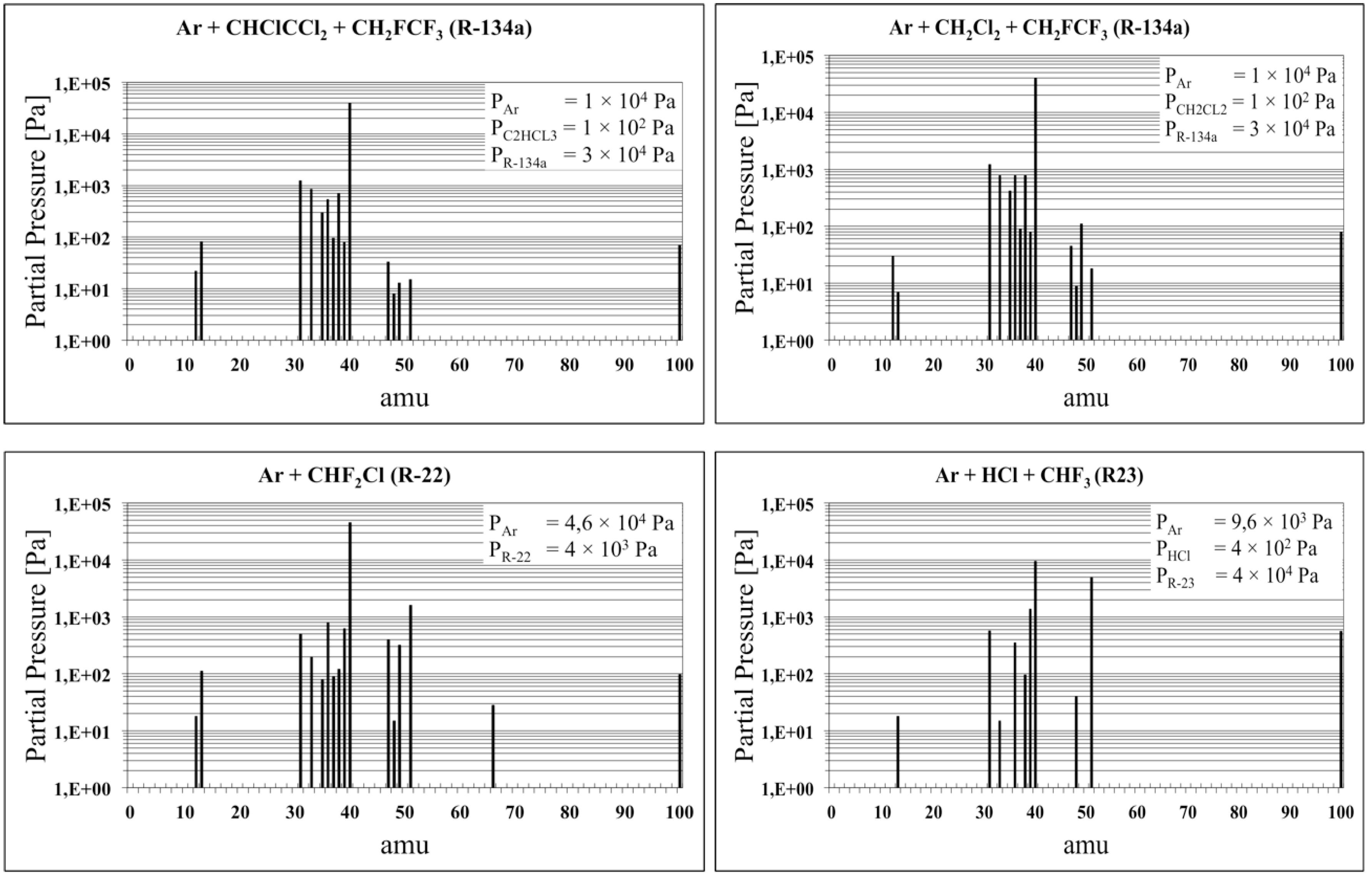
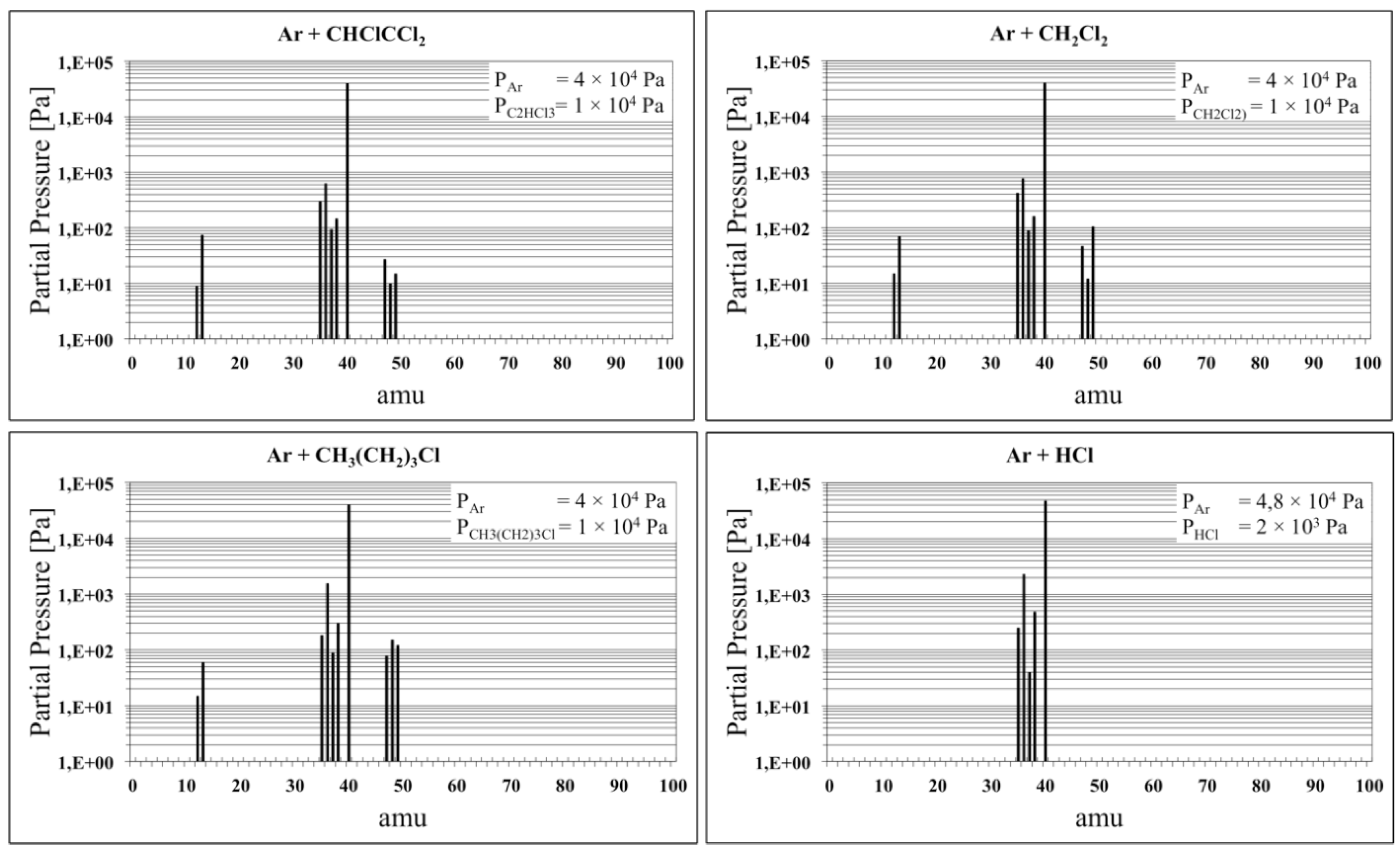
| Product of Dissociation | |||||||
|---|---|---|---|---|---|---|---|
| Substance | Amu | Substance | Amu | Substance | Amu | Substance | Amu |
| C(n) | 12 | 35Cl(n) | 35 | HF2(i) | 39 | CH2Cl(i) | 49 |
| CH(i) | 13 | H35Cl(n)/36Ar(n) | 36 | 4Ar(n) | 40 | CHF2(i) | 51 |
| CH2F(i) | 31 | 37Cl(n) | 37 | CCl(i) | 47 | CF35Cl(i) | 66 |
| CH2F(i) | 33 | H37Cl(i) | 38 | CHCl(i) | 48 | C2F4(n) | 100 |
| (n) = neutral; (i) = ionic | |||||||
| Treatment Conditions | Photovoltaic and Diode Parameters | ||||||
|---|---|---|---|---|---|---|---|
| Temperature [K] | Pressure [Pa] | Time [min] | Nr of Cells | Rs * [ohm] | Rsh * [ohm] | Efficiency [%] | |
| LCHY | Ar | ||||||
| CHClCCl2 (1,1,2-Trichloroethylene) | |||||||
| 673 | 200 | 4.98 × 10⁴ | 15 | 25 | 1.8 ± 0.9 | 87 ± 11 | 9.3 ± 1.1 |
| 500 | 4.95 × 10⁴ | 10 | 19 | 1.5 ± 0.4 | 59 ± 9.3 | 5.7 ± 1.7 | |
| CH2Cl2 (Dichloromethane) | |||||||
| 673 | 100 | 4.99 × 10⁴ | 15 | 25 | 2.2 ± 0.9 | 82 ± 9.9 | 8.8 ± 0.9 |
| 500 | 4.95 × 10⁴ | 10 | 22 | 1.1 ± 0.6 | 63 ± 8.7 | 6.5 ± 1.5 | |
| CH3(CH2)3Cl (1-Chlorobutane) | |||||||
| 673 | 200 | 4.98 × 10⁴ | 15 | 20 | 1.8 ± 1.1 | 77 ±12 | 7.8 ± 1.4 |
| 500 | 4.95 × 10⁴ | 10 | 23 | 0.9 ± 0.5 | 58 ± 11 | 5.4 ± 2.2 | |
| Fluorinated Hydrocarbons | |||||
|---|---|---|---|---|---|
| Trade Name | Name | Chemical Formula | Trade Name | Name | Chemical Formula |
| R-23 | Trifluoromethane | CHF3 | R-32 | Difluoromethane | CH2F2 |
| R-125 | Pentafluoroethane | CHF2CF3 | R-134a | 1,1,1,2-Tetrafluorethane | CH2FCF3 |
| R-143a | 1,1,1-Trifluoroethane | CH3CF3 | R-152a | 1,1-Difluoroethane | CH3CHF2 |
| Photovoltaic and Diode Parameters | ||||
|---|---|---|---|---|
| Gas Mixture | Nr of Cells | Rs * [ohm] | Rsh * [ohm] | Efficiency [%] |
| Ar + CHClCCl2 + R-134a | 23 | 1.2 ± 0.02 | 1657 ± 20 | 15.7 ± 0.5 |
| Ar + CH2Cl2 + R-134a | 32 | 1.5 ± 0.04 | 1550 ± 9 | 14.6 ± 0.5 |
| Ar + R-22 | 50 | 0.8 ± 0.01 | 1870 ± 5 | 15.8 ± 0.3 |
| Ar + HCl + R23 | 50 | 1.1 ± 0.01 | 1900 ± 5 | 16.2 ± 0.2 |
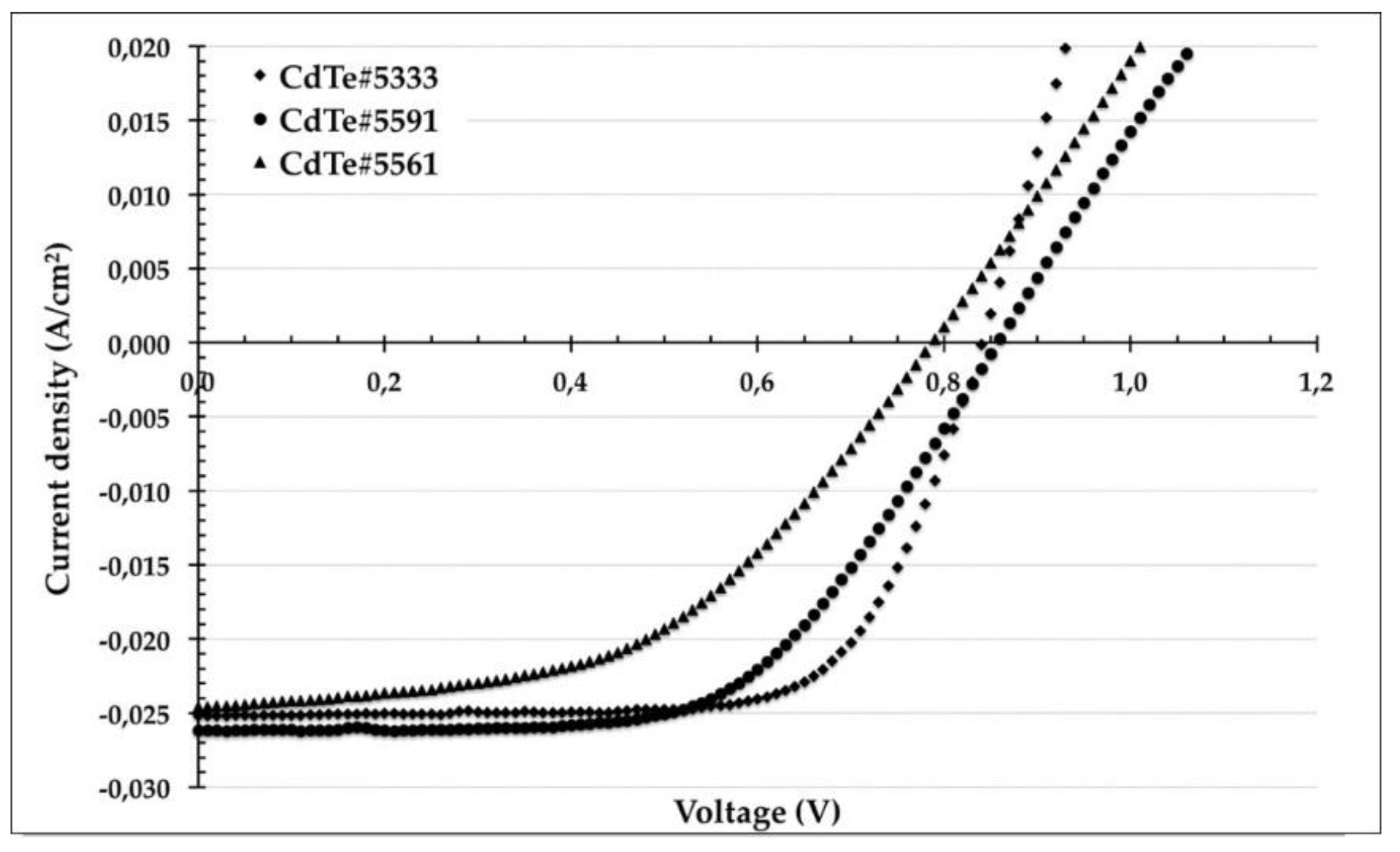
| Sample | Voc (mV) | Jsc (mA) | FF (%) | Eff. (%) | Rs * [ohm] | Rsh * [ohm] |
|---|---|---|---|---|---|---|
| # 5333 | 830 | 25.2 | 70.01 | 14.94 | 5.6 ± 0.02 | 1428 ± 20 |
| # 5591 | 860 | 26.1 | 59.2 | 13.19 | 10.6 ± 0.04 | 1250 ± 9 |
| # 5561 | 786 | 24.5 | 50.4 | 9.36 | 14.2 ± 0.01 | 227 ± 5 |
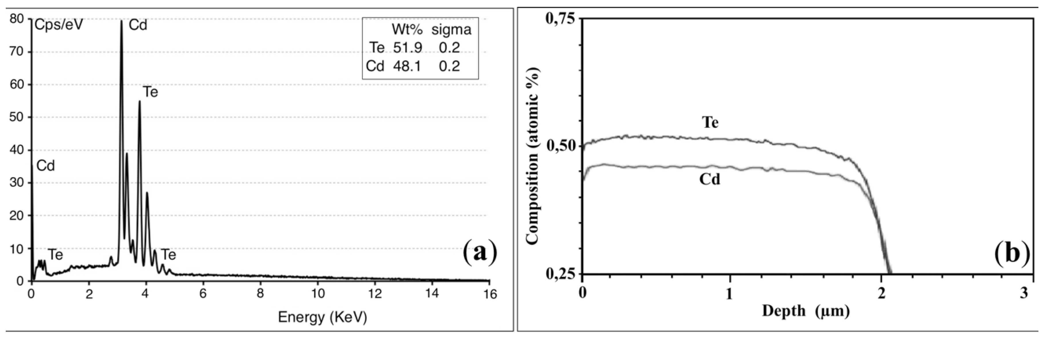
| EDX Scan Along Grain Boundary | EDX Scan Inside Grain | |||||||
|---|---|---|---|---|---|---|---|---|
| # | S | Cl | Cd | Te | # | S | Cd | Te |
| 1 | 29.3 | 4.9 | 42.4 | 23.4 | 1 | 4.4 | 46.2 | 49.4 |
| 2 | 16.1 | 4.8 | 35.0 | 44.1 | 2 | 3.2 | 47.3 | 49.5 |
| 3 | 24.4 | 4.0 | 45.4 | 26.2 | 3 | 2.1 | 48.2 | 49.7 |
| 4 | 17.1 | 5.1 | 44.7 | 33.1 | 4 | 3.0 | 47.3 | 49.7 |
| 5 | 3.2 | 47.7 | 49.1 | 5 | 2.3 | 47.8 | 49.8 | |
| 6 | 2.9 | 50.7 | 46.4 | 6 | 48.5 | 51.5 | ||
| 7 | 2.9 | 49.3 | 47.8 | 7 | 51.2 | 48.8 | ||
| 8 | 2.5 | 49.4 | 48.1 | 8 | 51.3 | 48.7 | ||
| 9 | 2.8 | 49.7 | 47.5 | |||||
| 10 | 3.0 | 49.2 | 47.8 | |||||
| 11 | 2.7 | 50.8 | 46.5 | |||||
© 2016 by the authors; licensee MDPI, Basel, Switzerland. This article is an open access article distributed under the terms and conditions of the Creative Commons by Attribution (CC-BY) license (http://creativecommons.org/licenses/by/4.0/).
Share and Cite
Bosio, A.; Rosa, G.; Menossi, D.; Romeo, N. How the Chlorine Treatment and the Stoichiometry Influences the Grain Boundary Passivation in Polycrystalline CdTe Thin Films. Energies 2016, 9, 254. https://doi.org/10.3390/en9040254
Bosio A, Rosa G, Menossi D, Romeo N. How the Chlorine Treatment and the Stoichiometry Influences the Grain Boundary Passivation in Polycrystalline CdTe Thin Films. Energies. 2016; 9(4):254. https://doi.org/10.3390/en9040254
Chicago/Turabian StyleBosio, Alessio, Greta Rosa, Daniele Menossi, and Nicola Romeo. 2016. "How the Chlorine Treatment and the Stoichiometry Influences the Grain Boundary Passivation in Polycrystalline CdTe Thin Films" Energies 9, no. 4: 254. https://doi.org/10.3390/en9040254
APA StyleBosio, A., Rosa, G., Menossi, D., & Romeo, N. (2016). How the Chlorine Treatment and the Stoichiometry Influences the Grain Boundary Passivation in Polycrystalline CdTe Thin Films. Energies, 9(4), 254. https://doi.org/10.3390/en9040254