1. Introduction
Commercial development of photovoltaic systems requires a technology which is efficient, reliable, and low cost. CdTe/CdS thin film solar cells satisfy all the aforementioned requirements [
1]. Progress has been made in improving the efficiency of CdTe/CdS research devices, where a final recorded efficiency of 21.5% has been obtained [
2] in the laboratory. Light absorption and charge separation in thin-film polycrystalline cadmium telluride (CdTe) photovoltaic (PV) solar cells largely occur in the vicinity of the CdS/CdTe interface [
3]. Interdiffusion between CdS and CdTe at the interface occurs during the deposition of the CdTe layer, especially when using a high temperature deposition technique, and/or during CdCl
2 heat treatment. This interdiffusion is bidirectional, but there is more sulfur diffusing into the CdTe than Te diffusing into the CdS [
4]. The solid solution formed in the CdTe side of the junction is CdS
xTe
1−x where x refers to the concentration of S and it is Te-rich with p-type conductivity, while that formed in the CdS side of the junction is CdS
1−yTe
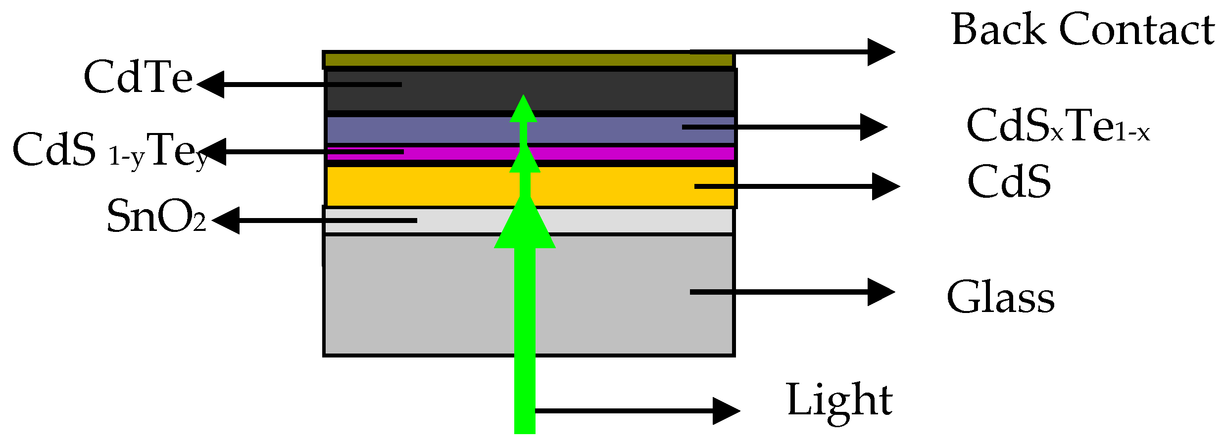
y, where y refers to the concentration of Te and it is S-rich with n-type conductivity. A schematic of the superstrate CdS/CdTe thin film solar cell is illustrated in
Figure 1, where the solid solutions on both sides of the CdS/CdTe heterojunction are shown.
Light reaches the CdTe absorber layer through the glass substrate, transparent conductive oxide (SnO
2), and the window (CdS layer) passing through these solid solutions. The formation of the Te-rich CdS
xTe
1−x at the CdS/CdTe interface is important for efficient PV devices. That is, it modifies the spectral response of the solar cell [
5], reduces the lattice mismatch at the CdS/CdTe junction [
6] which is about 9% [
7], and reduces the number of interfacial states and recombination centers [
8,
9]. The n-type CdS
1−yTe
y could be beneficial to the diminishment of the carrier recombination rate around the CdS/CdTe junction by shifting the electrical junction away from the high recombination hetero-interface between the CdS and the interdiffusion layer [
10], and it can reduce the CdS film thickness, which can be beneficial for window transmission, but also it can reduce the short wavelength optical transmission of the window layer resulting in a poor spectral response in this wavelength region [
11,
12]; this could lead to reduced performance of the solar cell. It can also result in lateral junction discontinuities, and non-uniform consumption of the CdS window layer. Another influence of alloying at the CdS/CdTe junction is that the lattice parameters will change due to the formation of CdTe
1−xS
x and CdS
1−yTe
y solid solutions in the absorber and window layers.
The non-uniform consumption of CdS can be mitigated by CdCl
2 heat treatment of the CdS layer prior to CdTe deposition to increase the density and size of CdS grains, to reduce grain boundary diffusion, and to sharpen the CdS optical transmission edge. Forming oxides on the CdS layer suppresses the Te interdiffusion from CdTe to the CdS film and the formation of a CdS
1−yTe
y alloy [
13]. That is, oxides reside on grain surfaces and penetrate grain boundaries.
Polycrystalline CdS
xTe
1−x and CdS
1−yTe
y thin films can be produced by several methods such as: thermal evaporation [
14,
15,
16,
17,
18], RF magnetron sputtering [
16], brush plating [
17], pulse plating [
19], pulsed laser deposition [
20], closed space sublimation (CSS) [
21,
22,
23,
24], metal organic chemical vapor deposition MOCVD [
25], chemical bath deposition (CBD) [
26], and spray pyrolysis (SP) [
27,
28] by first producing CdS films then annealing them in nitrogen atmosphere in the presence of tellurium vapor. This last method was used in this work to produce the S-rich CdS
1−yTe
y thin films on glass substrates. The films were doped with indium because the CdS window layer in our solar cells was doped with indium to improve its electrical conductivity. Hence the S-rich solid solution in the solar cell contains indium.
From the above it is apparent that a complete understanding of the compositional, structural, electrical, and optical properties of the intermixed layers CdS
xTe
1−x (Te-rich) and CdS
1−yTe
y (S-rich) that usually constitute the interfacial region in the CdS/CdTe solar cell is essential. Several authors [
4,
15,
19,
21,
29,
30,
31] produced and characterized Te rich CdS
xTe
1−x thin films. For example, Marymathelane
et al. [
29] produced nanocrystalline CdS
xTe
1−x at different temperatures and studied their optical properties. Pal
et al. [
31] studied the electrical conductivity, thermoelectric and optical properties along with microstructural properties of CdS
xTe
1−x films. According to our knowledge there is little information about the production and characterization of S-rich CdS
1−yTe
y thin films [
21,
27,
28], so there is a need for extensive studies about the production, and properties of S-rich CdS
1−yTe
y solid solutions to understand their influence on solar cell performance. The aim of this work is to review the production and properties of this material in the form of thin films when produced by the spray pyrolysis method on glass substrates.
4. Structure, Composition, and Morphology
The CdS-CdTe solid solutions can grow in the cubic (zinc blende) phase, the hexagonal (wurtzite) phase or the mixed (cubic and hexagonal) phase [
14]. CdTe
1−xS
x has the crystallographic form of the zinc blende (ZB) structure with space group (F-43m), and CdS
1−yTe
y the wurtzite (WZ) with space group (P63mc) structure. The mixed phase of the CdS-CdTe system shows a large miscibility gap that depends on temperature in which both phases (cubic and hexagonal) are present.
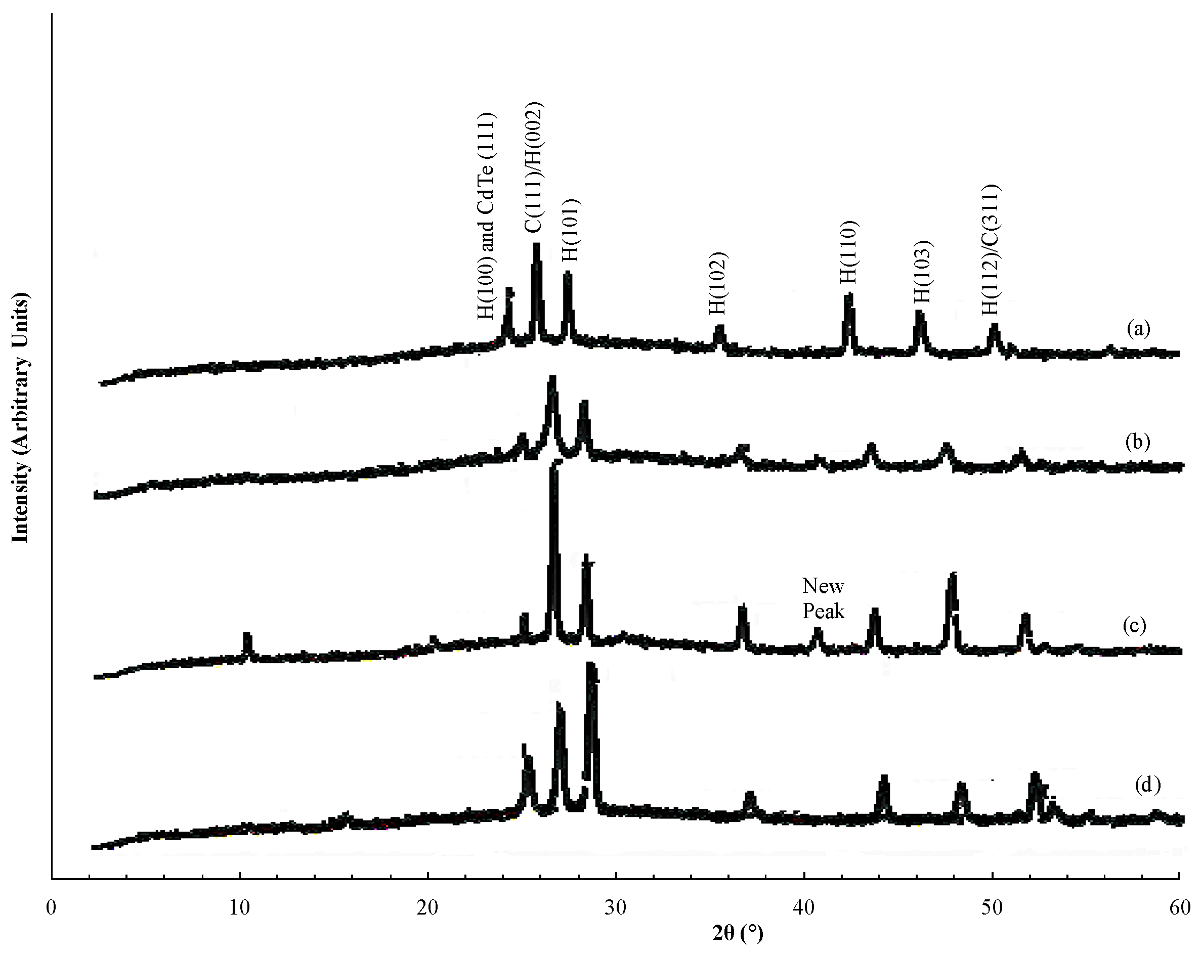
To determine the structure of the films, XRD diffractograms for three films with different Te content and hence different colors (
Figure 3a–c) were recorded at room temperature and shown. In addition, the X-ray diffractogram of a film of pure CdS:In is shown (
Figure 3d).
Figure 3a has the greatest Te content (darkest red color), and
Figure 3c has the smallest Te content (lightest yellow-red color). As the Figure shows, the CdS:In film displays the mixed (cubic and hexagonal structure). The CdS
1−yTe
y displays all reflection peaks of CdS:In present in diffractogram
Figure 3d, but with a shift in the positions of all peaks towards smaller angles with the increase in Te content. This indicates that the lattice spacing d, and hence lattice parameters increase with the increase of Te content in the films. In addition, a satellite peak located at 2θ = 40.8° appeared in the diffraction patterns of films (
Figure 3c) and (
Figure 3b) which is related to the CdS
1−yTe
y alloy. This result is opposite to that for the Te rich CdS
xTe
1−x solid solution, where d decreases with the increase in S content. This is shown by different authors such as; Pal
et al. [
31] who found a shift in the position of the (002) peak in the XRD diffractograms of CdS
xTe
1−x films from 2θ = 24.3° to 25.3° with change in composition (0.1 < x < 0.8). Birkmire
et al. [
5] who studied the diffusion of S in CdTe films reported a shift in the position of the C(111) peak of CdTe towards larger 2θ values and found a decrease in the lattice parameters of the CdTe/CdS cells after CdCl
2 heat treatment. They attributed these changes to the formation of a CdTe
1−xS
x solid solution. Nakayama
et al. [
17], who studied sulfur diffusion within CdTe, found that the positions of CdTe peaks are slightly shifted and observed satellites. Murali
et al. [
19] showed that the variation of lattice spacing and lattice parameters with composition is linear and obeys Vegard’s law [
16]. For another set of films, EDS was used to determine the composition. The concentrations of tellurium [Te], sulfur [S], and indium [In] in the films were obtained from the EDS reports, and used to find the molar ratio y, where y = [Te]/([S] + [Te]), and the percentage ratio of the concentration of indium to that of cadmium ([In]/[Cd])% in the films. The values of y are inserted in
Table 1 besides the thickness of the films and the percentage ratio of indium to cadmium in the solution.
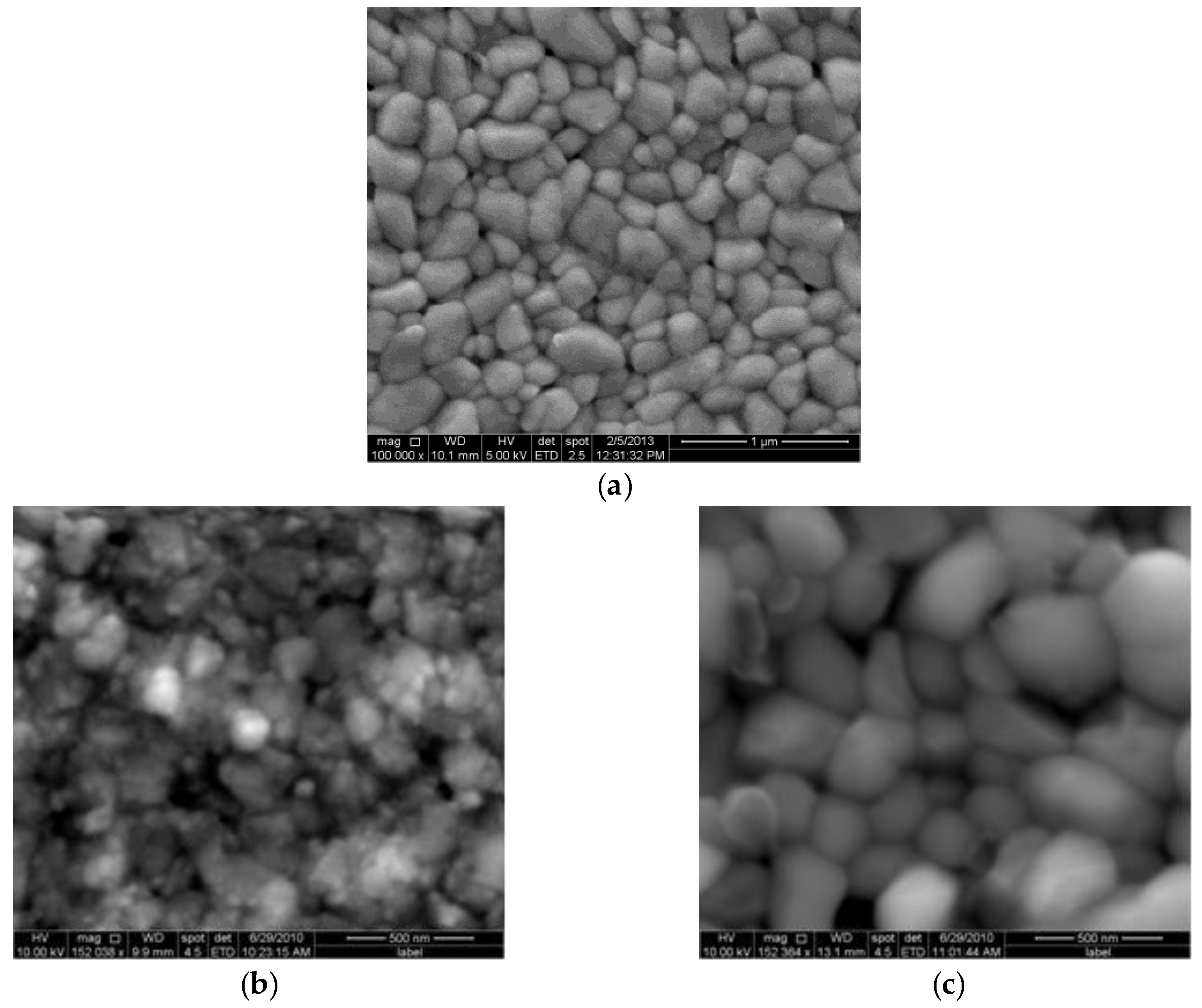
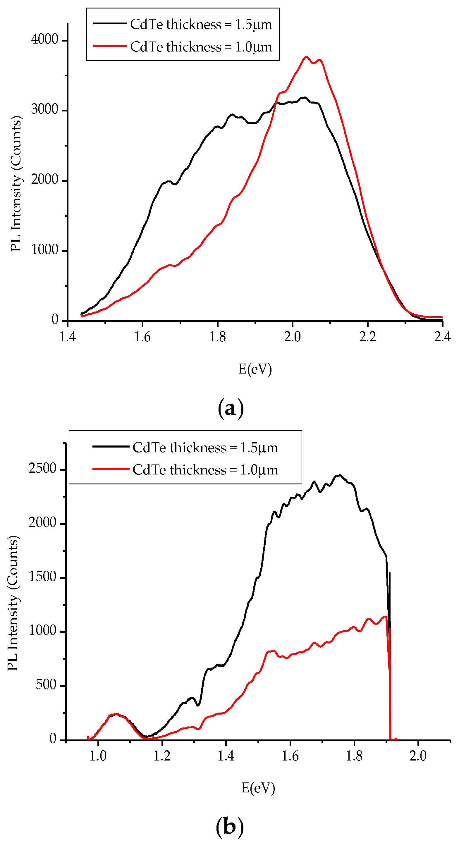
Figure 4 displays the scanning electron microscope observations for a CdS:In film (
Figure 4a), and another two CdS
1−yTe
y films with comparable thickness but different Te concentration (t = 720 and 620 nm with y = 4.51 × 10
−2 and 28.45 × 10
−2, respectively) (
Figure 4b,c)). The three films are polycrystalline, but the difference between the morphologies of the CdS:In film and the CdS
1−yTe
y films is apparent.
The grains of the CdS:In film are large (100–200 nm) and obvious, and the film appears to be compact and uniformly covered with material. On the other hand, the surface of the CdS
1−yTe
y film in
Figure 4b appears to consist of smaller grains and aggregates of smaller grains, while the CdS
1−yTe
y film in
Figure 4c appears with morphology close to that of the CdS:In film, but it shows larger grains with wider size distribution (135–625 nm). Both CdS
1−yTe
y films contain pores, but the film in
Figure 4c is more compact than that in
Figure 4b, where the ImageJ software was used to find the circularity ratio as a measure of compactness of both CdS
1−yTe
y films. It is found to be 0.563 for the image in
Figure 4b, and 0.614 for the image in
Figure 4c, indicating that the film in
Figure 4c has higher Te concentration and it is thinner.
5. Transmittance, Absorbance and Optical Parameters
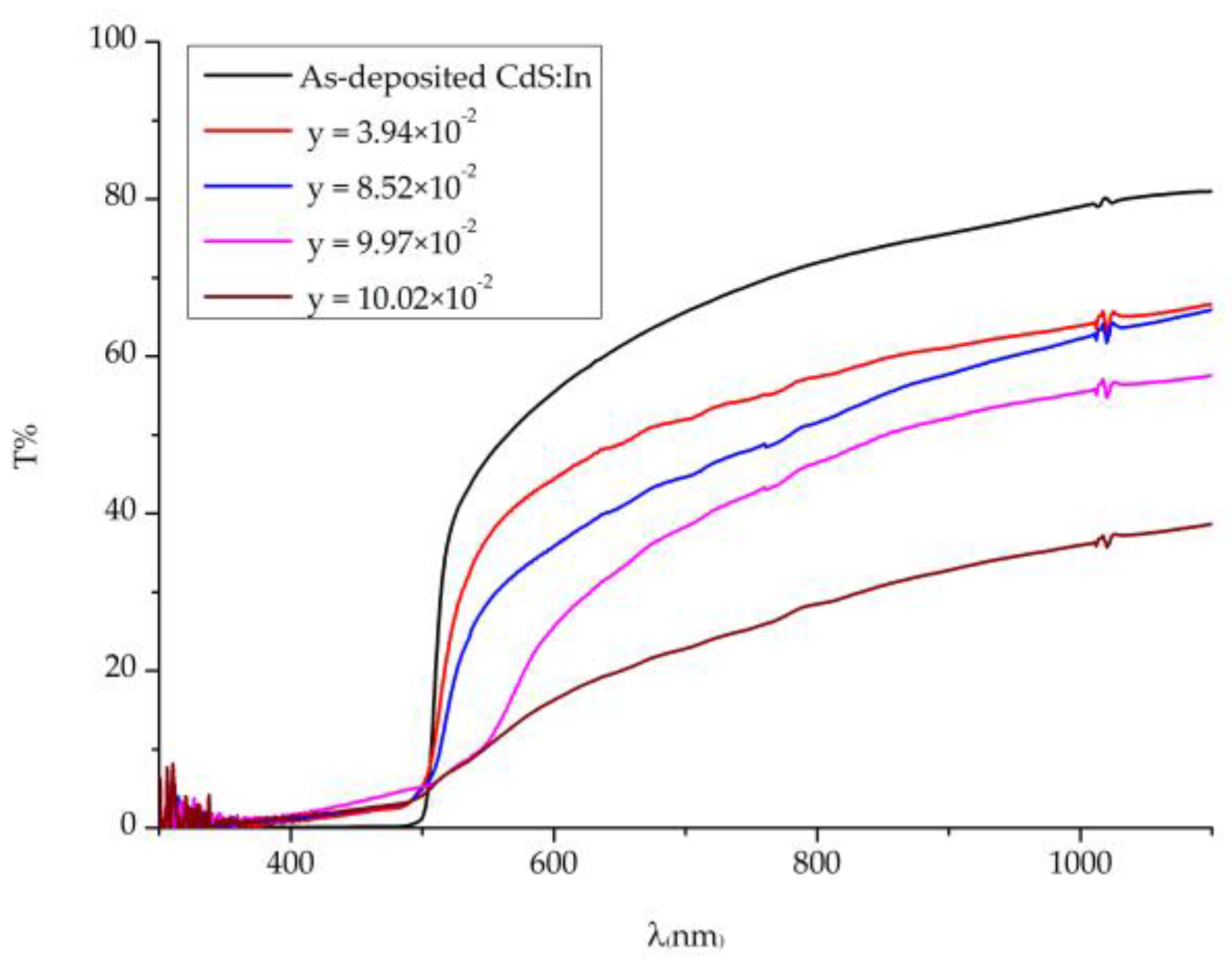
Figure 5 displays the transmittance T% of CdS
1−yTe
y thin films of different composition and comparable thickness besides that of a CdS:In film, which was recorded at room temperature in the 290–1100 nm wavelength range. As the figure shows, the CdS:In film shows the highest transmittance, and T% of all CdS
1−yTe
y films decreases with the increase of y, so the increase of Te content in the films results in the increase of the absorbance, and the decrease of transmittance. In addition, it is obvious from the figure that, with the increase of y, the absorption edge shifts towards longer wavelengths, and its sharpness decreases. That is, with the increase of Te in the films the absorption edge shifts from the absorption edge of CdS (2.5 eV) to that of CdTe (1.5 eV) [
36].
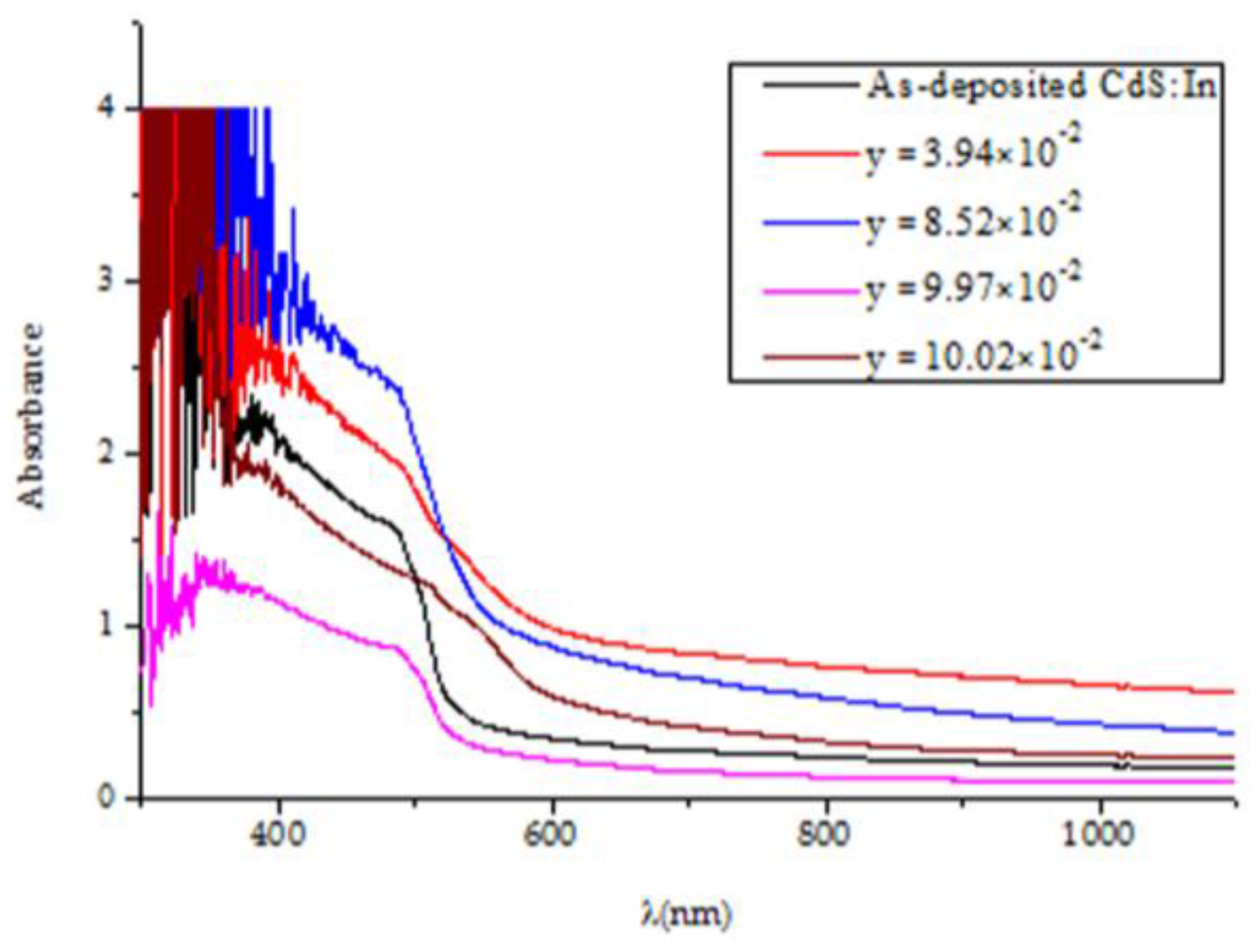
Figure 6 displays the absorbance of the CdS
1−yTe
y thin films and that of the CdS:In film. Comparing the absorbance of the films on the small wavelength side, it is noticed that the largest absorbance is that of the film of y = 8.52 × 10
−2, where it has a thickness of 465 nm, and [In]/[Cd]% of 3.84 ± 0.63, then that of the film with y = 3.49 × 10
−2, thickness 490 nm, and [In]/[Cd]% of 2.98 ± 0.20. The smallest absorbance is that of the film with y = 9.97 × 10
−2 that has a thickness of 420 nm and [In]/[Cd]% of 2.75 ± 1.88. The explanation of these results is that the increase of thickness, Te content and In content increase the absorbance. The net absorbance depends on the combined influence of these three factors. The film of largest absorbance has the largest indium content and comparable thickness with that of y = 3.49 × 10
−2, which has a smaller indium content. The film of smallest absorbance has the largest Te content, but the smallest thickness and the smallest indium content in the set. The absorption edges for the films are not sharp, but each curve contains two absorption edges. This means that two bandgaps are present in each case (the one of the hexagonal phase and that of the cubic phase). The sharpest absorption edge is that of the CdS:In film. Dense oscillations before the cutoff wavelength of CdS:In (≈514 nm for pure CdS) are observed, which are evidences on the presence of quantum dots [
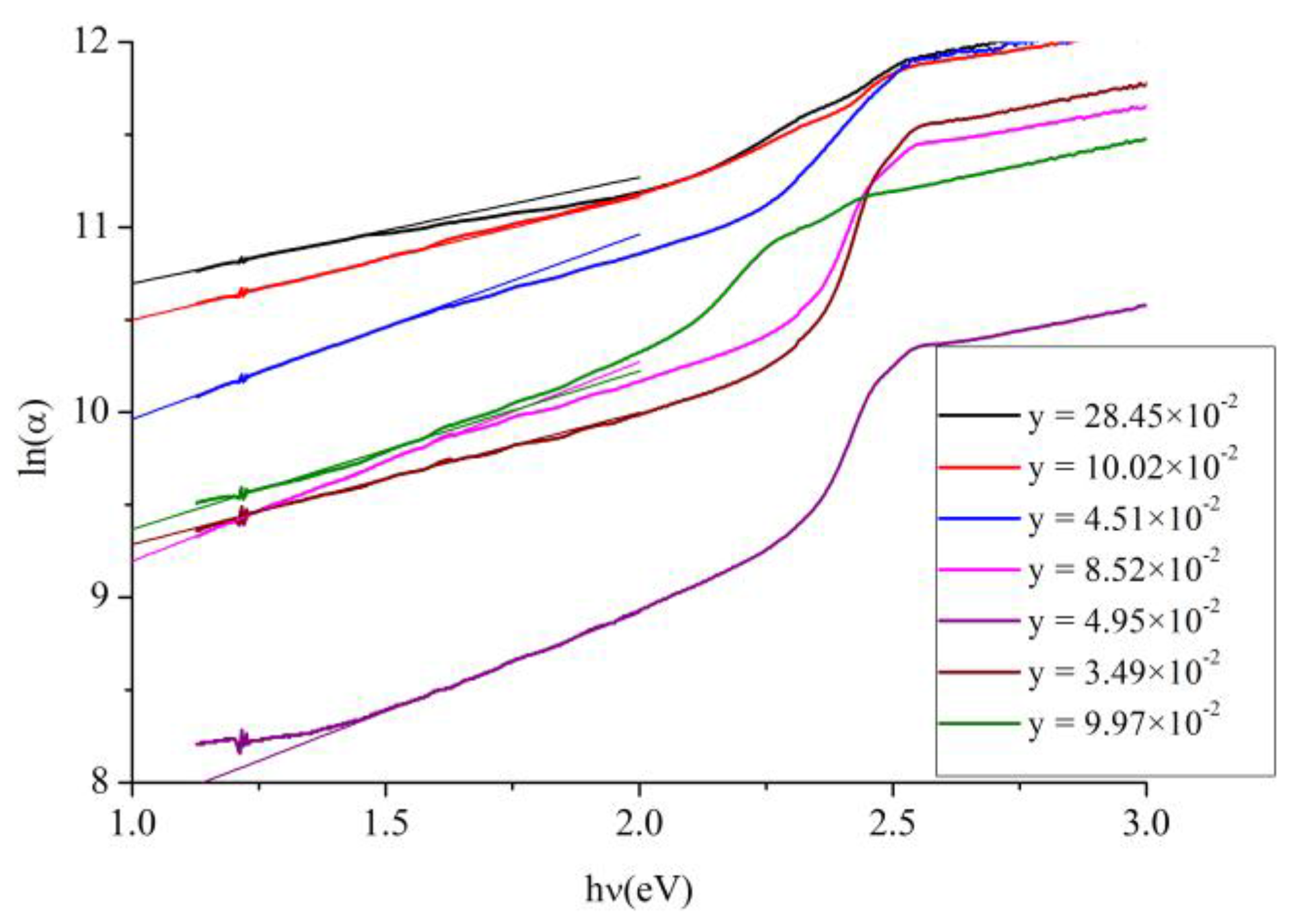
37]. Tailing is obvious in the bandgaps of the films, and it is not possible to find a monotonic relation between absorbance and composition due to the differences in film thickness and indium content of the films. In the following paragraphs, the bandgap energy and tailing in the bandgap will be estimated and discussed.
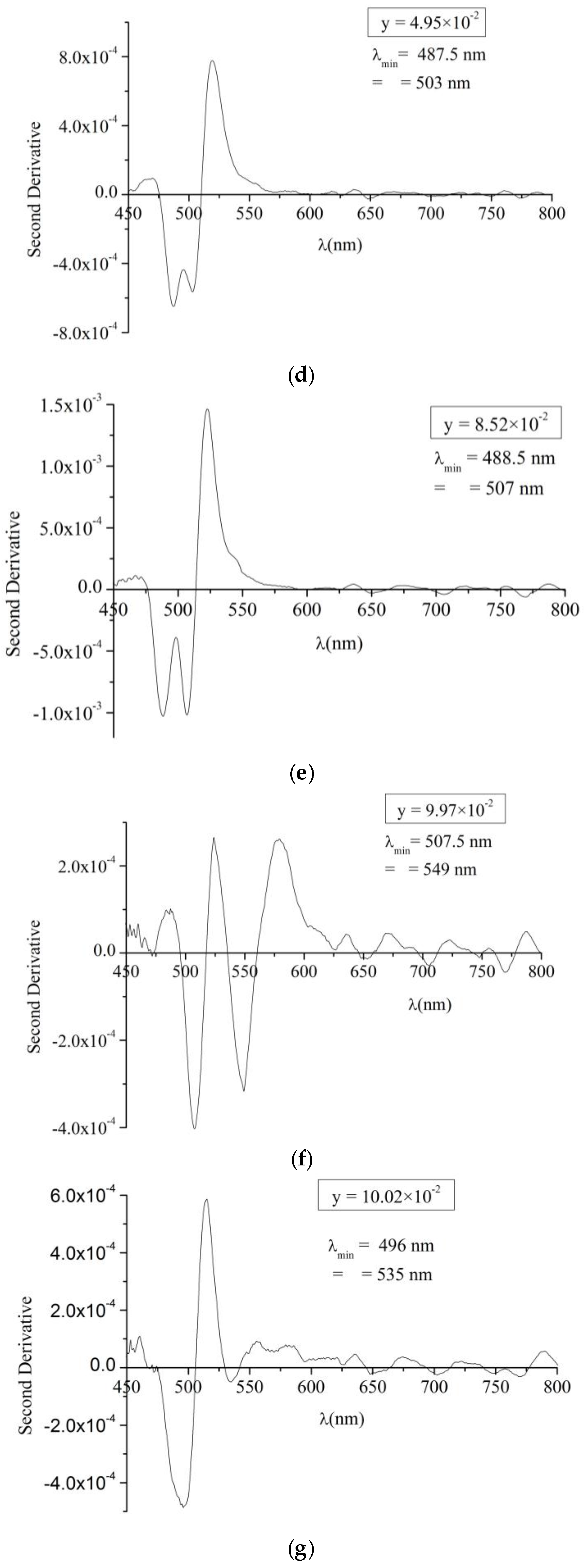
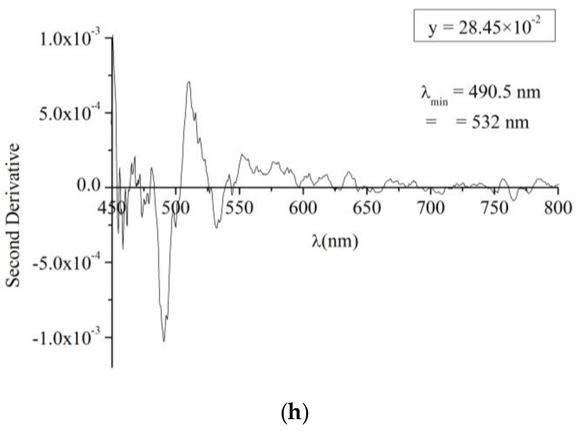
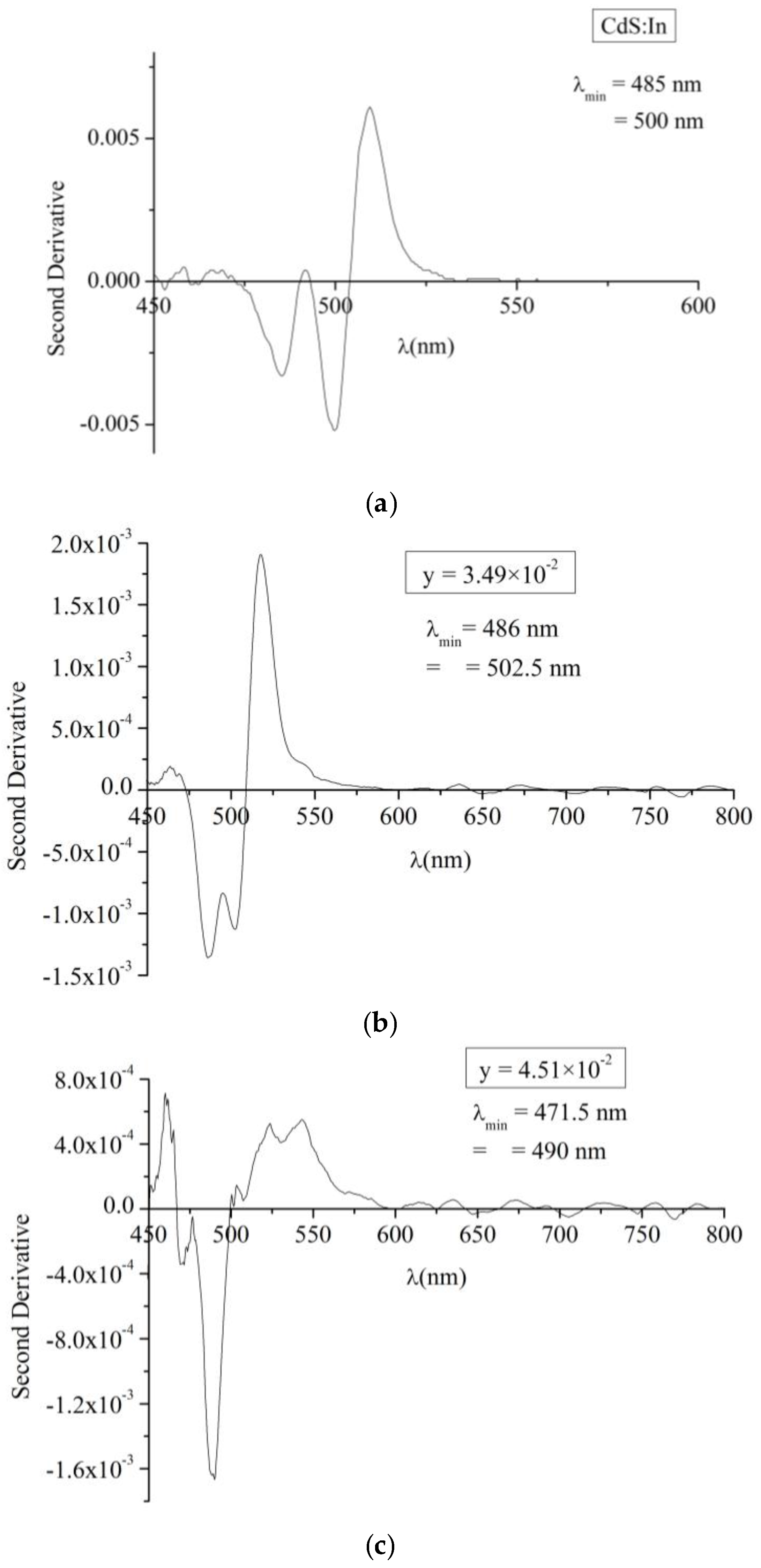
To determine the bandgap energy of the produced CdS
1−yTe
y solid solution, the second derivative of the absorbance was deduced from the transmittance and displayed in
Figure 7. The minima in the second derivative refer to the maxima in the absorbance and they indicate the values of the bandgap energies present in the solid solution. For comparison, a similar graph for a pure CdS:In thin film was displayed in
Figure 7a. Two minima at λ = 500 and 485 nm are observed for the pure CdS:In beside a shoulder at λ = 480.5 nm. These are the same three minima observed by Nĕmec
et al. [
38] for CdS films prepared by chemical bath deposition, but the positions of these minima in their work are shifted towards shorter wavelengths. The shift is due to the size effect, where their films are nanocrystalline with radii in the range 2.6 to more than 10 nm.
According to Nĕmec
et al. [
38], these minima are in good agreement with the splitting of the valence band (A, B, C) at the centre of the Brillouin zone which is typical of the bulk CdS in hexagonal structure. This confirms that the CdS:In films under study in this work also contain the hexagonal phase, which is consistent with the XRD diffractograms. This result is expected, because the films were prepared at high substrate temperature (490 °C). By comparing the second derivative curves of CdS
1−yTe
y thin films with that of the CdS:In thin film in
Figure 7a, it is found that the films showed the hexagonal phase alone for y ≤ 8.52 × 10
−2, and a mixed (cubic and hexagonal phase for 9.97 × 10
−2 ≤ y ≤ 28.45 × 10
−2). Hence two bandgaps were deduced from the second derivative curves; one for the hexagonal and the other for the cubic phase. The positions of the minima deduced from
Figure 7 and the estimated values of the optical bandgap energies are inserted in
Table 2, besides the values of film thickness for the whole set of films. From the table it can be noticed that the hexagonal bandgap decrease with increasing y from 2.48 eV for y = 0 (pure CdS:In) to a minimum of 2.443 eV at y = 9.97 × 10
−2 then increases with y and reaches 2.528 eV at y = 28.45 × 10
−2. Also from the Table it can be noticed that the cubic bandgap energy increases with y from 2.259 eV at y = 9.97 × 10
−2 to 2.331 eV at y = 28.45 × 10
−2, so graded bandgaps are obtained by varying the composition of the CdS
1−yTe
y solid solution, in a way similar to the intermixing at the CdS/CdTe junction, which results with a graded region in which the bandgap depends on composition.
The explanation of these results is complicated, because the values of y obtained by the EDS analysis are not trustworthy, and because of the differences in indium content of the films. The effect of increasing indium content is to increase the bandgap, or in other words, to shift the minima to lower wavelengths, but qualitatively these results have a trend that is consistent with the model used by Ohata
et al. [
30] and Pal
et al. [
31], which they obtained for the bandgap of the Te-rich CdS
xTe
1−x alloy. In this model, the bandgap of the alloy can be predicted using a simple quadratic equation:
Hence the bandgap of the S-rich CdS
1−yTe
y alloy will be given by:
where
is the bowing parameter and its theoretical value is 2 [
31].
Several experimental results are consistent with Equation (1) for CdS
xTe
1−x [
16,
19,
39], but according to our knowledge, there are no experimental or theoretical results for CdS
1−yTe
y. For CdS
xTe
1−x alloy, Duenow
et al. [
16] found that the bandgap decreases below the CdTe bandgap value of E
g(CdTe) = 1.5 eV, to as low as 1.41 eV at x ≅0.3, before increasing at higher x values. Ohata
et al. [
39] have shown that the bandgap of CdS
xTe
1-x alloy decreases with addition of S in the Te-rich region for values of x up to 0.25. In addition, Murali
et al. [
19] observed that the bandgap shifts towards CdS side as the concentration of CdS in the films increases, and got a bandgap that varies from 1.44 to 2.41 eV as the percentage of CdS increased. On the other hand, for CdS
xTe
1−x nanocrystalline thin films, Marymathelane
et al. [
29] got E
g values in the range of 1.54–2.32 eV for films of different composition and observed that the bandgap shifts towards CdS side as the concentration of CdS in the films increases, which may mean that they did not got quadratic relation between E
g and x.
In the low photon energy range it is assumed that the spectral dependence of the absorption edge follows the empirical Urbach rule given by [
40,
41]:
where
α0 is a constant,
Ee denotes an energy which is constant or weakly dependent on temperature and is often interpreted as the width of the tail of localized states in the bandgap. Therefore, to investigate this tailing, the absorption coefficient
α was estimated from the transmittance measurements for the whole set of films, and the relation between the natural logarithm of the absorption coefficient
ln(α) and photon’s energy
hν was plotted and shown in
Figure 8. A linear fit was performed in the low energy region, from which the values of
Ee were estimated for all values of y and the results are inserted in
Table 2. As the Table shows the values of
Ee are large. The explanation of this is that low Te concentrations are known to create midgap levels in CdS [
4]. In studying photoconductive lifetime of CdS used in thin film solar cells, Ahrenkiel
et al. [
7] found that the amplitude of the photoconductive signal is reduced by about an order of magnitude for Te doped CdS in comparison to pure CdS and the initial lifetime of the Te doped CdS is shorter than that of the pure CdS. They explained this result by saying that the effect of Te is to trap holes and act as either deep traps or recombination centers. This interpretation supports the results of this work in that it is a main reason for the large values of
Ee. We did not find in the literature experimental or theoretical values of
Ee for CdS
1−yTe
y or CdS
xTe
1−x to compare these results with them. So these results will be used as a reference. Pal
et al. [
31] plotted
ln(α) against photon’s energy from which they estimated the bandgap of the alloy, but they did not discuss tailing in the bandgap. By comparing
Figure 8 with their graph, it is noticed that they have sharper band edges. This confirms that they have just one bandgap and hence one phase for each value of x.
Reflectance
is related with transmittance by the relation
T + R =1. The reflectance was deduced from the transmittance data, and used to find the refractive index
n and the extinction coefficient
k by using the following relation [
18]:
where this definition is for the reflectance of a film for a light wave incident normally from air, with refractive index
, on a medium of complex refractive index
. Knowing the value of the absorption coefficient
which can be deduced from the transmittance, the extinction coefficient can be calculated using the relation:
where
is the wavelength in free space. Solving Equation (4) for the refractive index
n gives:
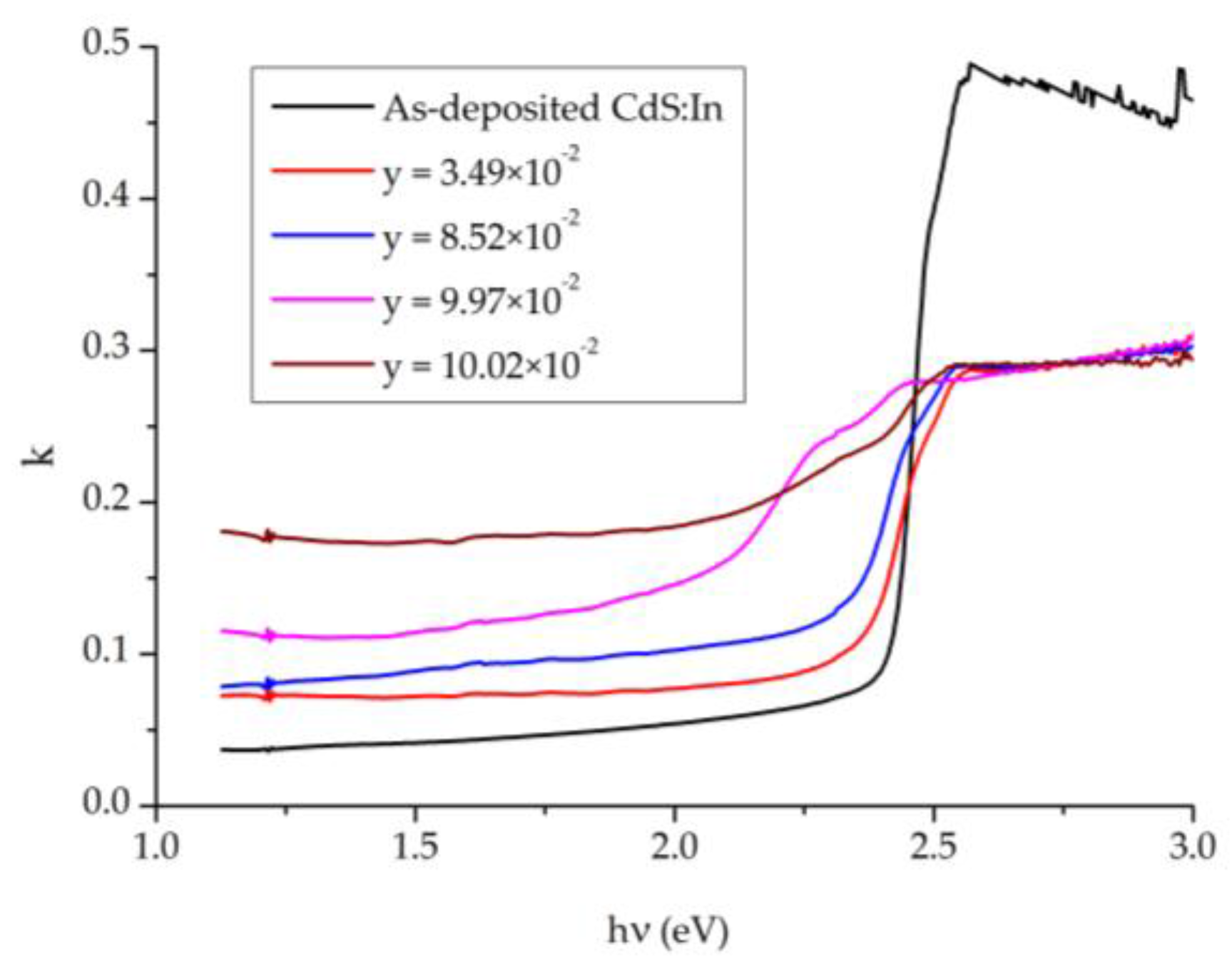
The extinction coefficient
k calculated from Equation (5) is plotted against the photon’s energy
and displayed in
Figure 9. The non-zero value of
k in the region before 2.5 eV (the fundamental absorption edge of CdS) can be interpreted by the extra absorption of light that occurs at the grain boundaries, where this is known for polycrystalline films [
42]. In this region
k is restricted in the range 0.042–0.174, where it increases with y. A sharp increase in
k occurs at the absorption edges which vary in sharpness according to y. The films with y = 9.97 × 10
−2 and y = 10.02 × 10
−2 show two absorption edges. These are due to the presence of a mixed phase in the films (cubic and hexagonal), where the cubic phase has a slightly smaller optical bandgap. After the sharp increase,
k becomes constant and equal to 0.291 for all CdS
1−yTe
y films, but for the CdS:In film it slowly decreases with
hν from 0.487 to 0.453 for the energy change from 2.5 to 3.0 eV.
The refractive index
n is calculated from Equation (6) and plotted against the photon’s energy
and displayed in
Figure 10. It is observed that
n increases slowly with
until the absorption edge, which is y dependent. After this, it strongly increases with
, and then reaches approximately a constant value—not shown in the figure. It is obvious that the sharpest absorption edge is that of the CdS:In thin film, then sharpness decreases with y. The shift of the absorption edge towards the side of lower energy is also observed. As the figure shows, for energies before ≈2.25 eV (the fundamental absorption edge), the refractive index increases slowly with y, and its value in this region at
hν = 1.5 eV—which corresponds to the bandgap energy of CdTe—lies in the range 2.10 for as-deposited CdS:In to 7.17 for the film of y = 10.02 × 10
−2.
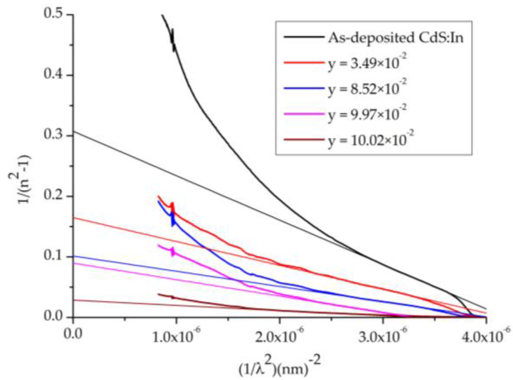
For energies below the absorption edge, refractive index dispersion can be analyzed by the single oscillator model, so the obtained refractive index n data is also analyzed to yield the long wavelength refractive index (
n∞) together with the average oscillator wavelength (
λ0) for CdS
1−yTe
y thin films of comparable thickness using the following relation [
42]:
The relation between
and
is shown in
Figure 11, beside the linear fits for the long wavelength side, where
,
and
are evaluated from the fit parameters and listed in
Table 3. From these values, the average excitation energy for electronic transitions
, and the dispersion energy which is a measure of the strength of interband optical transitions
, moments of the optical spectrum
and
are also calculated and listed in
Table 3 too, where
, and
. From
Table 3 it is observed that
,
,
,
and
increase with the Te content of the films represented by (y).
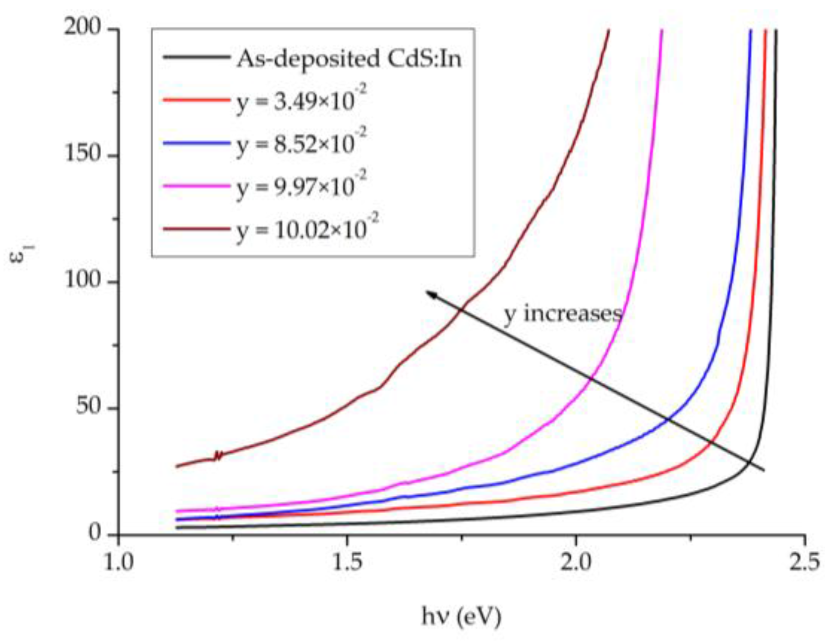
The complex dielectric constant (
is the orientation sum of the dielectric constant and the loss factor components with unity dimensions. The dielectric constants of the films have been evaluated from the following equations:
Figure 12 displays the real part of the dielectric constant
ε1 against the photon’s energy
for CdS
1−yTe
y films with comparable thickness but different composition y and a CdS:In film. In the region before 1.5 eV
ε1 increases with y, where it varies at
hν = 1.15 eV from 2.99–28.21. It increases gradually with photons’ energy until the absorption edge, where it increases sharply. The absorption edge moves towards lower energy with the increase in y. These observations are consistent with the behavior of the extinction coefficient
k and have the same explanations.
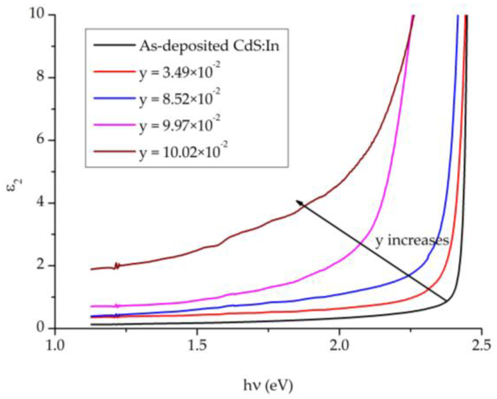
Figure 13 displays the imaginary part of the dielectric constant
ε2 against the photon’s energy
. In the low energy side at
it increases with y and varies in the range 0.127–1.913, and it increases slowly with photon’s energy. In the region of the absorption edge,
ε2 increases sharply with photon's energy, where the rate of increase decreases with y. The presence of the two phases of the CdS
1−yTe
y solid solution causes the decrease in the rate of increase of
ε2. In the high energy side after the fundamental absorption edge of CdS:In (2.5 eV),
ε2 becomes constant in consistence with the behavior of the refractive index
n. Both the real and imaginary parts of the dielectric constant show similar behaviors, but the imaginary part shows smaller values.


