1. Introduction
As a focus of public opinion in 2015, the “One Belt, One Road” project has attracted the eyes of the world, in which a fast and comfortable high-speed railway would connect the East with the West [
1,
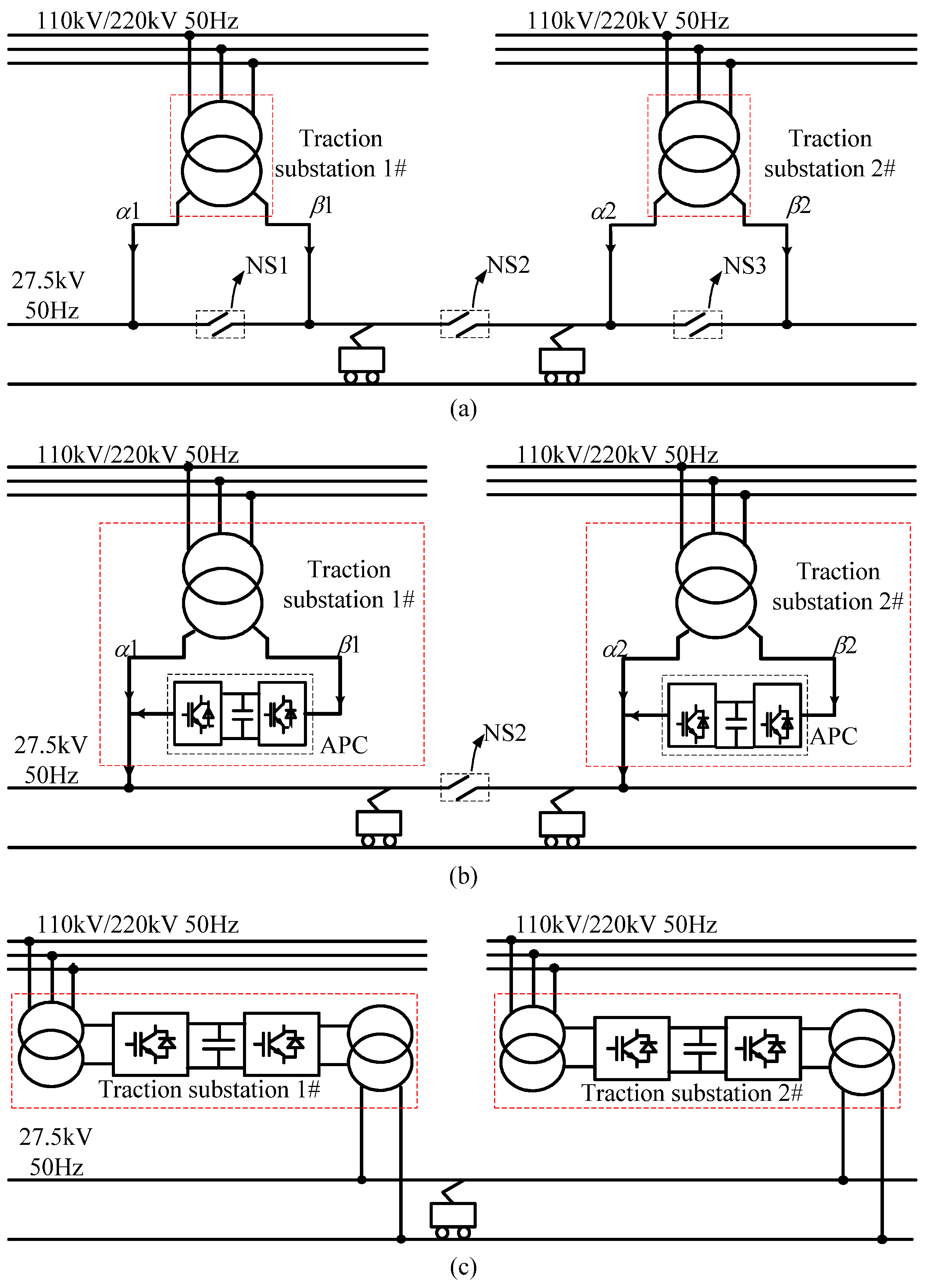
2]. The traction power supply plays one of the most important roles in a high-speed railway. The existing two-phase traction power supply in China is shown in
Figure 1a. In the traction substation, the voltage of the three-phase grid is transformed into two-phase voltage by a transformer [
3]. Due to the differences of phase, amplitude and frequency of the voltage between the adjacent arms α1 and β1 (α2 and β2), neutral sections must be set between the adjacent arms [
4]. There are mainly three problems caused by neutral sections: power quality issues such as unbalance, reactive power and low-order harmonics; disturbance between locomotive and network; speed loss of the locomotive. With the rapid development of high-speed railways, how to solve the aforementioned problems is a pressing problem.
The co-phase traction power supply system developed by Chinese scholars is analyzed in depth in [
5], which has been put into trial operation in Meishan, China. The structure of co-phase traction power supply is shown in
Figure 1b, where the neutral sections NS1 and NS3 could be canceled. The system solves the problems of power quality for electric railway with power electronic compensation devices—Active Power Compensators (APCs). Furthermore, the number of neutral sections is halved [
6].
In [
7], the advanced traction power supply system (ATPSS) based on a three-phase to single-phase converter is proposed, of which the system structure is shown in
Figure 1c. There is a step-down transformer on the input side and a step-up transformer on the output side in a traction substation, respectively. The system achieves a balanced three-phase grid load and controls the output of the traction network flexibly by using power electronics. Besides, the system could improve power quality and cancel the neutral sections totally, which is a new type of traction power supply system and a new exploration avenue in the related research. However, the output current is significantly uplifted in the light of step-down transformer ratio, which calls for more equipment requirements. In addition, due to the current restriction on the development of power electronic devices, the traditional two-level or tri-level or five-level structure couldn’t meet the requirements of the traction power supply system capacity. Nowadays, the research mainly focuses on how to enhance the system capacity. A multi-level cascade converter has the advantages of larger capacity and simpler control technique [
8,
9,
10], therefore, multi-level cascade converters can be applied to this system.
Consequently, in practical applications clamped multi-level converters mainly consist of three-level and five-level converters. Theoretically, any level of the output voltage could be obtained by cascading multiple converter modules. The output transformer in a traction substation of ATPSS can be canceled to enlarge the system capacity by means of cascading multilevel converters if the interface voltage level were higher than the output voltage level [
11,
12]. At the same time, if the number of cascade modules or the levels of multi-converter module were too large, it will cause difficulties in the design of the control system. It is important to work out a proper cascade system, especially for an engineering application of high reliability requirements [
13]. Along with the improvement of power electrical device, the new IGBTs (Insulated Gate Bipolar Transistor) make it possible that high-voltage and large-power applications come true, such as SiC and other devices described in [
14,
15].
Figure 1.
Traction power supply system modes: (a) The existing traction power supply system; (b) The co-phase traction power supply system; (c) The advanced traction power supply system.
Figure 1.
Traction power supply system modes: (a) The existing traction power supply system; (b) The co-phase traction power supply system; (c) The advanced traction power supply system.
According to the analysis above, a new traction substation based on a three-phase to single-phase cascade converter in ATPSS is proposed in this paper. The system inherits the advantages of the original traction substation in ATPSS. In this way, problems caused by the output transformer are solved and the interface voltage of the converter is improved to meet the requirements of traction substation capacity.
The paper is organized as follows:
Section 2 is dedicated to introducing the proposed three-level neutral point clamped (3L-NPC) cascade converter in a traction substation, and the 3L-NPC three-phase to single-phase is analyzed in detail. The simulation and experimental results are discussed in
Section 3. The conclusions are presented in the last part.
2. Configuration
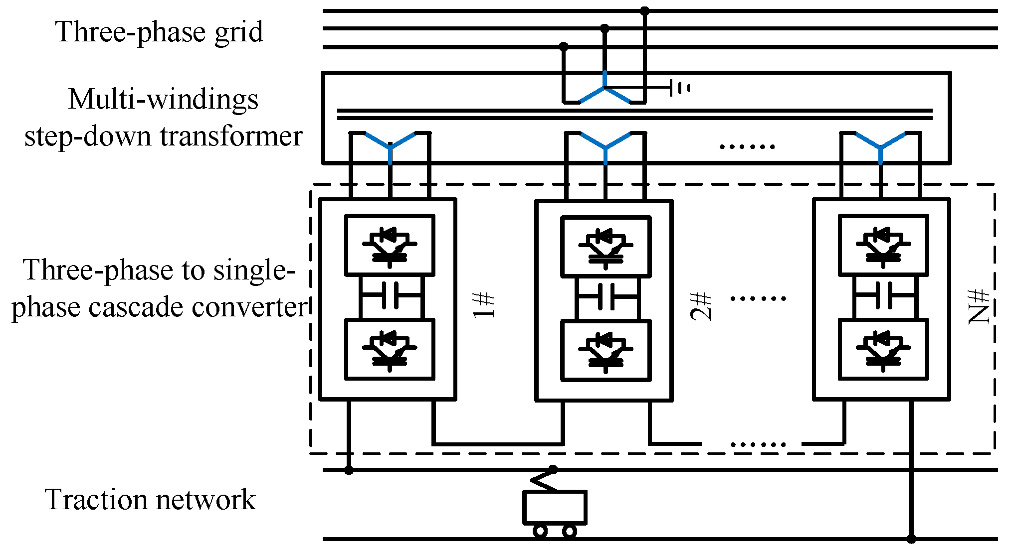
The proposed 3L-NPC cascade converter based on a three-phase to single-phase in a traction substation is shown in
Figure 2. The substation consists of a multi-windings step-down transformer connecting to the three-phase grid and several three-phase to single-phase AC-DC-AC converters, which are cascaded in the output terminal. The output of the system is an AC voltage satisfying the load requirements. The traction networks of the adjacent substations connect with each other to form the ATPSS. Meanwhile, the transformers provide isolated input voltages between different converters. Then the outputs of different converters can be connected in series and combined to generated one high voltage traction supply.
Figure 2.
The diagram of proposed traction substation system in advanced traction power supply system (ATPSS).
Figure 2.
The diagram of proposed traction substation system in advanced traction power supply system (ATPSS).
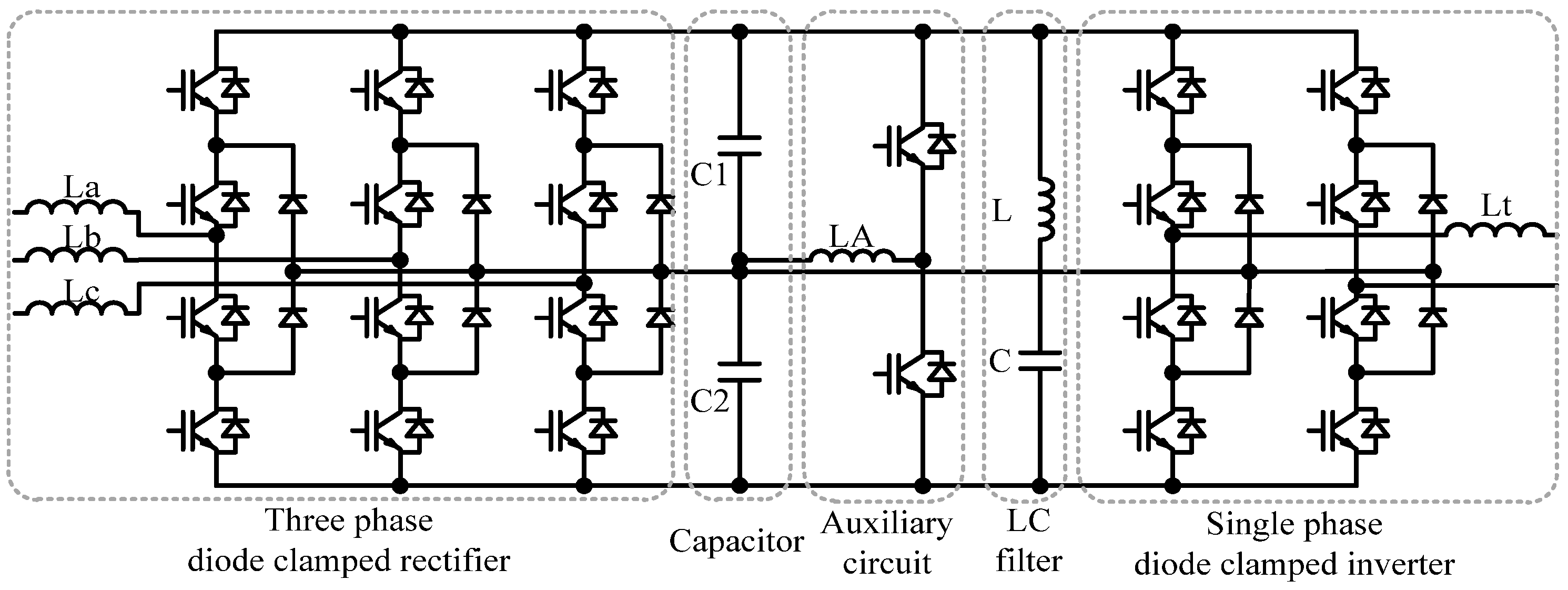
Owing to the limitations of the present level of power electronic devices, the cascade modules could output several times the voltage of a single module. The 3L-NPC three-phase to single phase converter configuration is shown in
Figure 3, taking the traction network capacity and the complexity of control strategy into consideration. The converter is made up of a three-phase 3L-NPC rectifier, auxiliary DC equalizing circuit, LC filter circuit, and single-phase 3L-NPC inverter. The three-phase and single-phase PWM converter can operate in four-quadrant mode, which is able to transfer energy on both sides of a three-phase to single-phase system. It’s realized that the system achieves active balanced current of the power grid using the three-phase PWM rectifier system. At the same time, the system provides network capacity in the same phase using a single-phase PWM inverter.
Figure 3.
Three-level neutral point clamped (3L-NPC) three-phase to single phase converter with equalizing circuit.
Figure 3.
Three-level neutral point clamped (3L-NPC) three-phase to single phase converter with equalizing circuit.
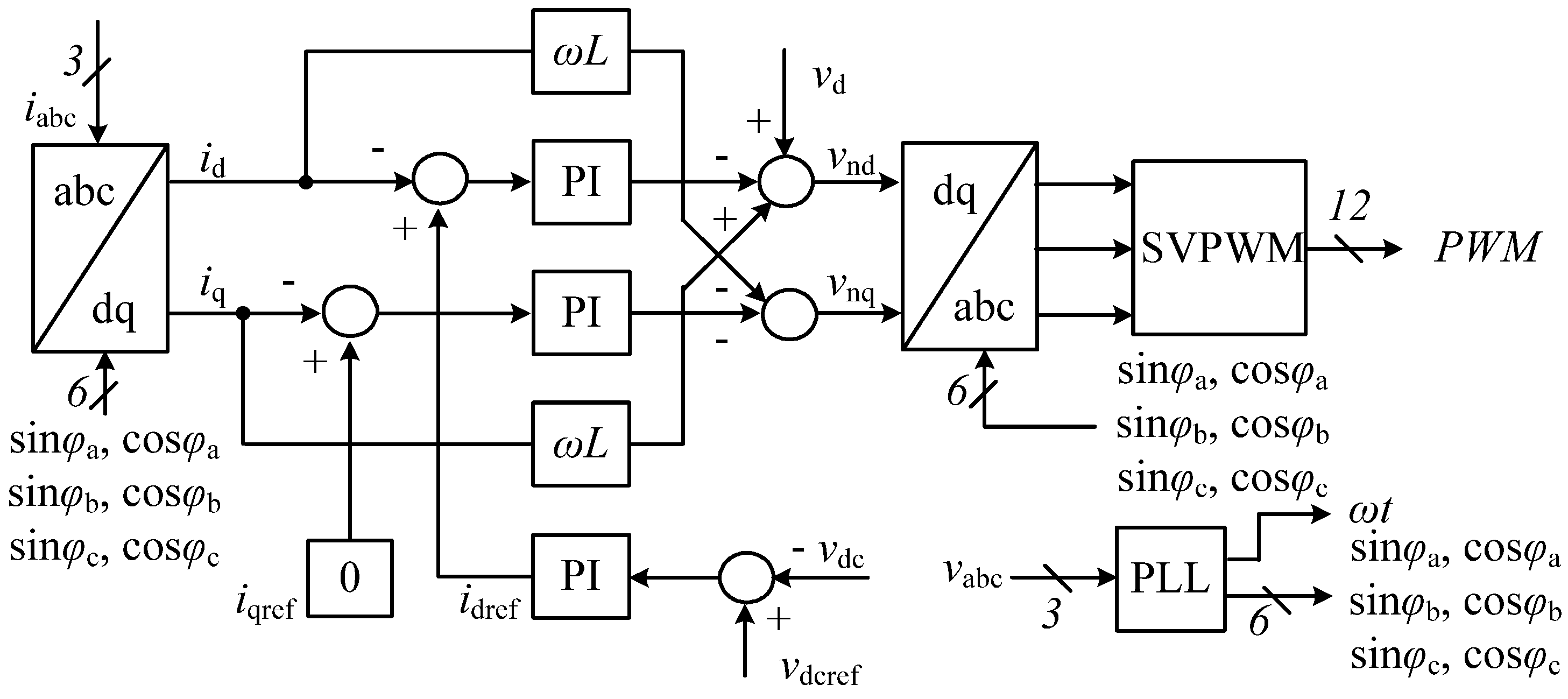
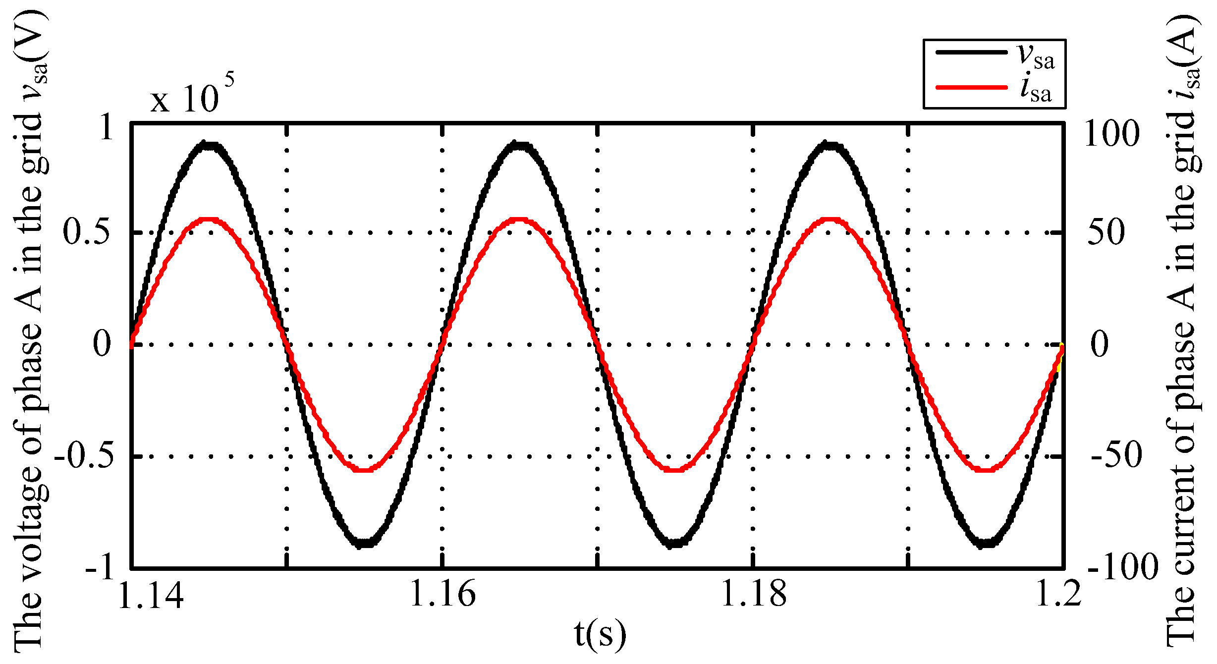
2.1. Control of Three-Phase Rectifier
The three-phase PWM rectifier operates under rectifier mode and active inversion mode in the four-quadrant with the traditional PWM rectifier control strategy [
16]. The system controls the active and reactive components of the input signals in the dq coordinate. Both the active current exchange between AC side and DC side and the stabilization control of DC voltage can be achieved. Specifically, a stable DC voltage is achieved by controlling the magnitude and direction of the active current between three-phase grid and the DC capacitor. The detail control principle is shown in
Figure 4.
Figure 4.
Block control diagram of the three-phase PWM rectifier.
Figure 4.
Block control diagram of the three-phase PWM rectifier.
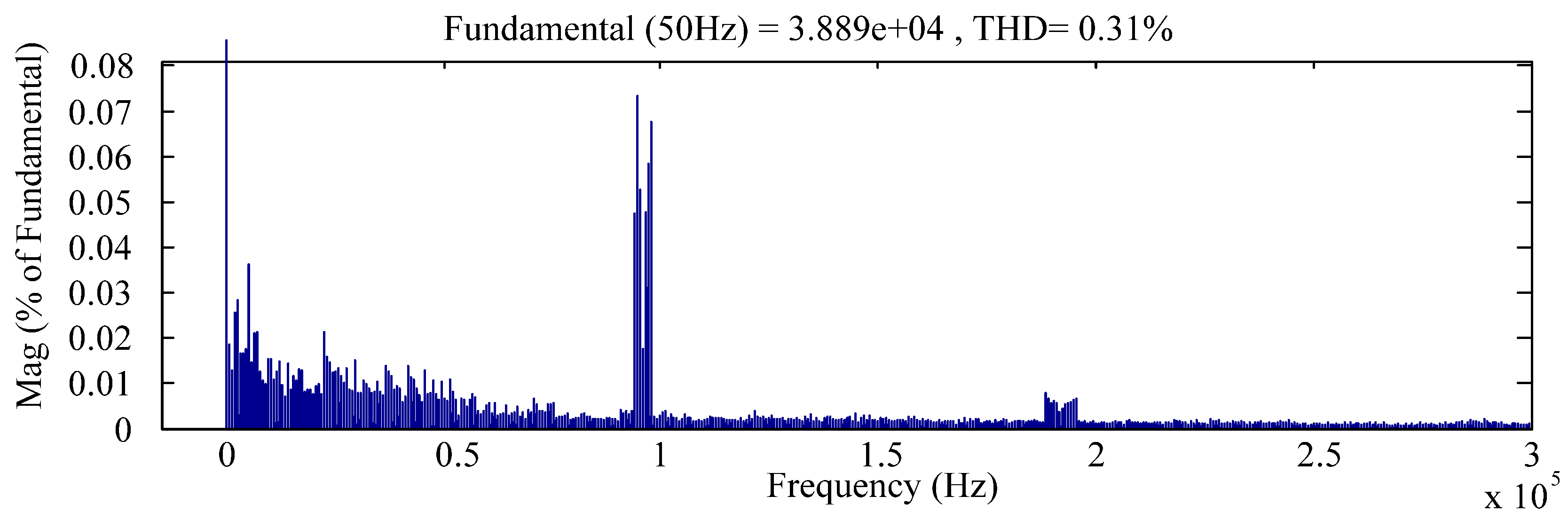
The grid current signal iabc is transformed into id and iq by the abc-dq transformation and the phase information of voltage vabc, which is acquired with a phase locked loop (PLL). Therefore, active and reactive power decoupling can be achieved. Then the DC voltage vdc is compared with a given reference voltage vdcref. The error of vdc and vdcref will go through PI (proportional integral) controller and then compared with the d component of the three-phase current, then the result will go through another PI controller as an output current. In the meanwhile, the q component of the three-phase current is compared to a given value 0, and the PI controller output a value, which controls the q component of the command signal. Then the dq components of the voltage are obtained using the mathematical relationship between the current and voltage after the inverse transformation. Afterwards, the switch control signals will be accomplished with a space vector PWM (SVPWM) control module. By the operation above, the stability of the DC voltage can be achieved. Furthermore, it’s able to ensure that rectifier is operating under the unity power factor and the impact on power quality of the public traction network will be reduced.
2.2. Control of Single-Phase Cascade Inverter
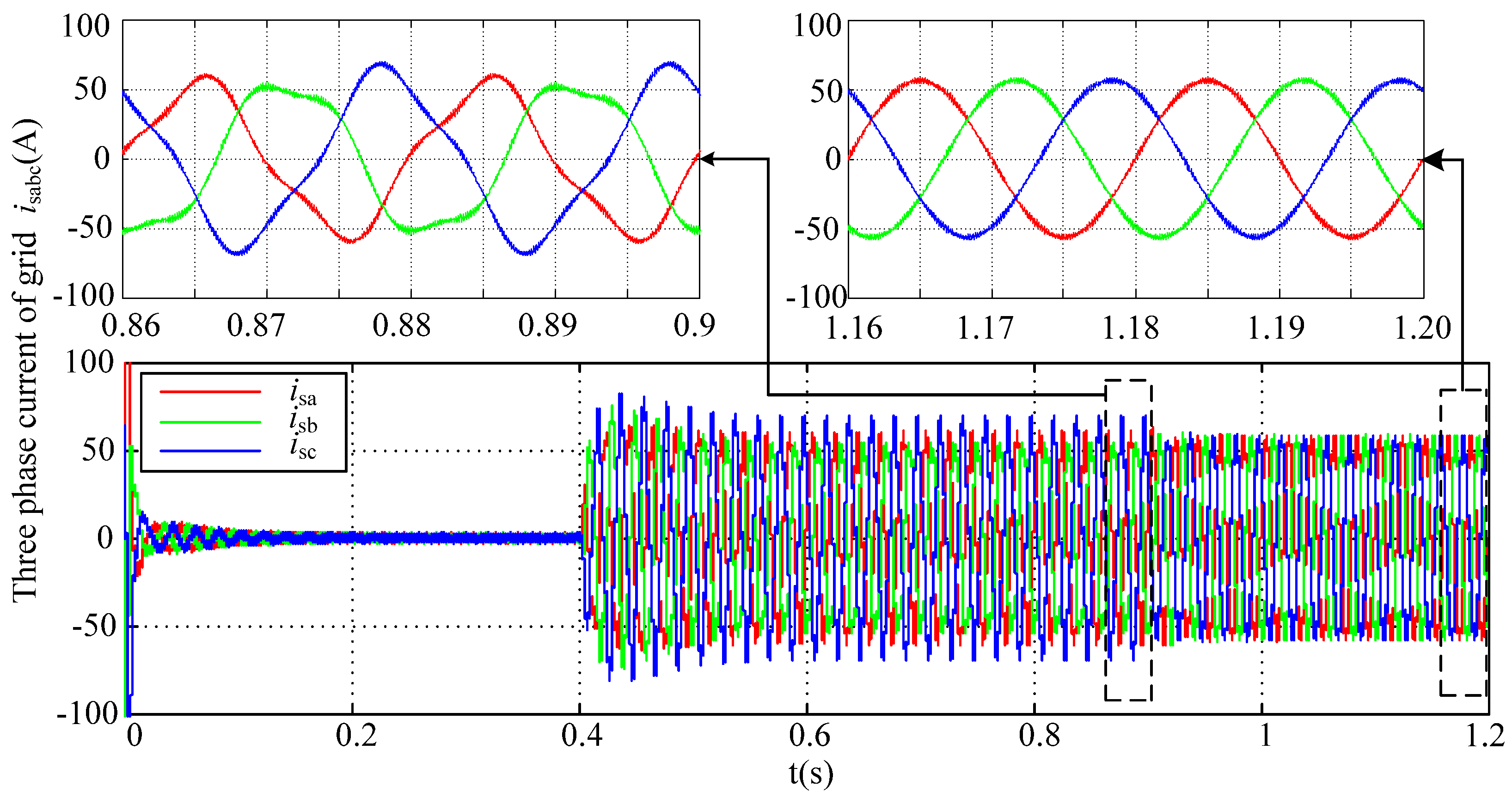
Assuming that the traction network is working properly, ATPSS requires the cascade converter could actively connect to the traction network and maintain the stability of the port voltage amplitude and frequency in the traction network. Besides, the converter can provide active and reactive current depending on the load requirements and satisfy the need that multiple substations can be automatically assigned current according to the load and the impedance of the traction network. Therefore, the single-phase PWM inverter output voltage can be equivalent to a voltage source, whose frequency, phase and amplitude are adjustable.
The number of inverter cells N depends on the desired output voltage level, which is synthesized by adding up all the H-bridge cells output voltage as vo = vo1 + vo2 + vo3 + … + voN. In a cascade system that utilizes equal sets of DC sources (Vdc1 = Vdc2 = Vdc3 = … = VdcN), the number of output voltage levels is N × (m−1) + 1, where N is the number of cascade cells and m is the number of output voltage levels in each multilevel H-bridge cells, here m = 5.
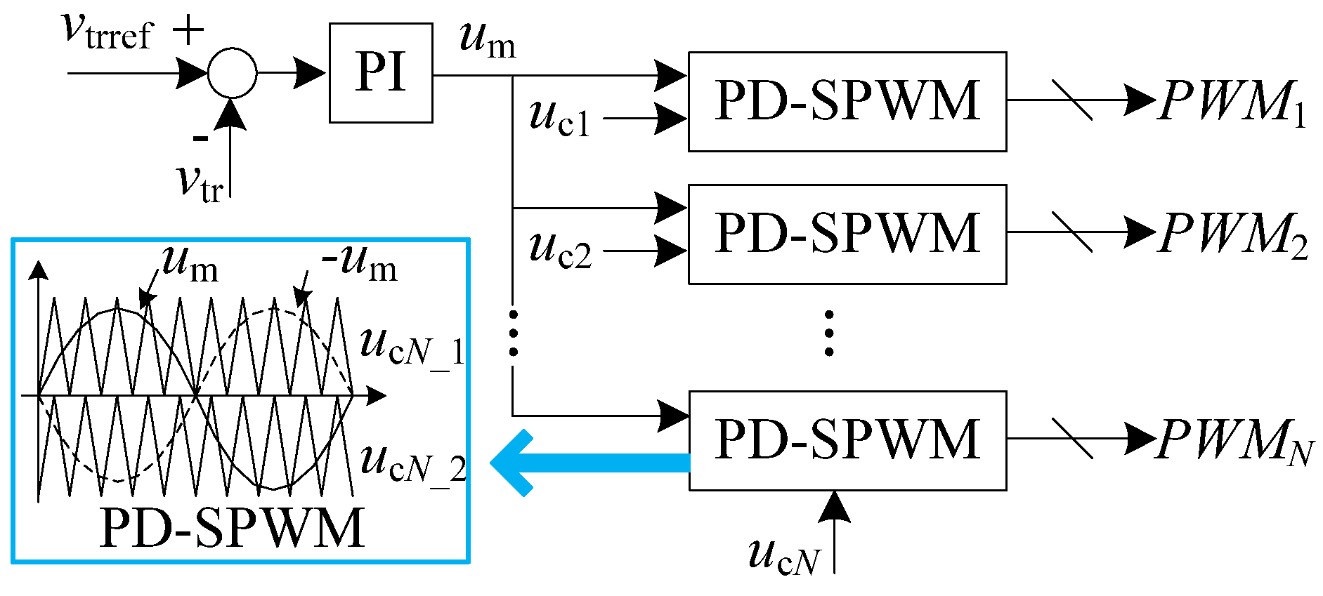
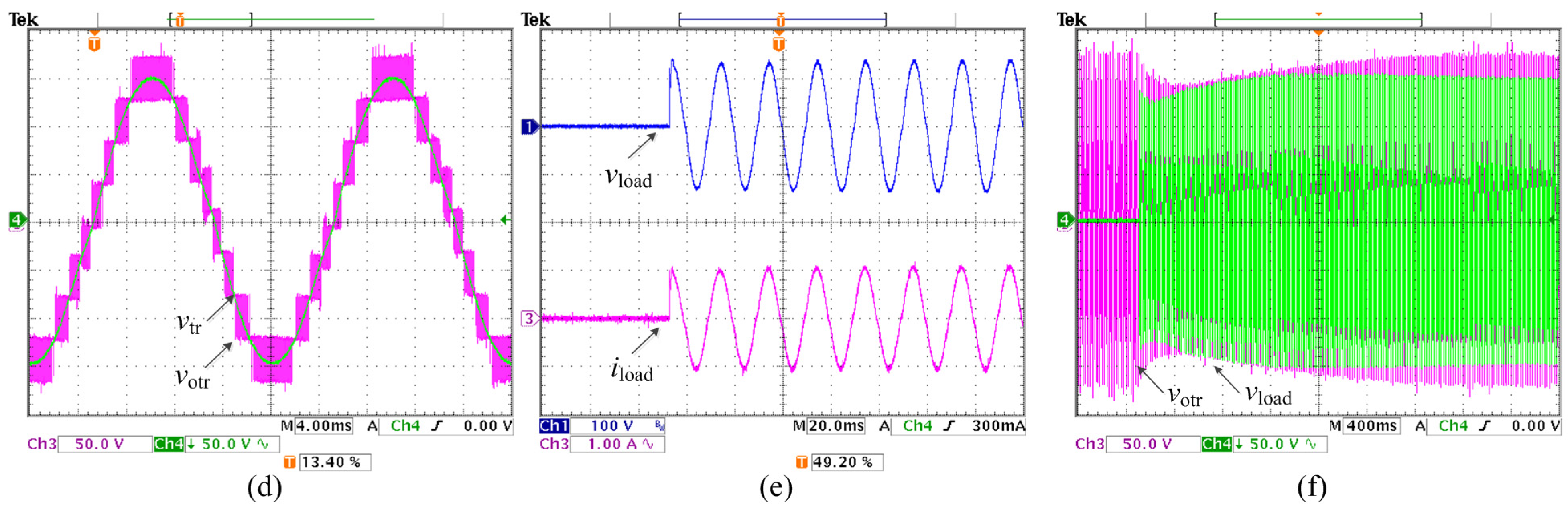
It is necessary to get a controllable amplitude, frequency and phase voltage source model in the ATPSS. In this paper, the outer voltage could make a stable modulation. The control principle is shown in
Figure 5.
vtr, that is referred as traction network detected actual voltage, is compared with
vtrref recognized as a given reference voltage. The result passes the PI controller and its output operates as a co-modulated wave (
um) of each 3L-NPC three-phase to single-phase converter module. Carrier (
ucN) is calculated by phase carrier shift SPWM (PSC-SPWM) technique. Inverter modulation method used in the 3L-NPC three-phase to single-phase converter module is phase disposition SPWM (PD-SPWM) [
17].
Figure 5.
Block control diagram of the single-phase PWM (pulse width modulation) cascade inverter.
Figure 5.
Block control diagram of the single-phase PWM (pulse width modulation) cascade inverter.
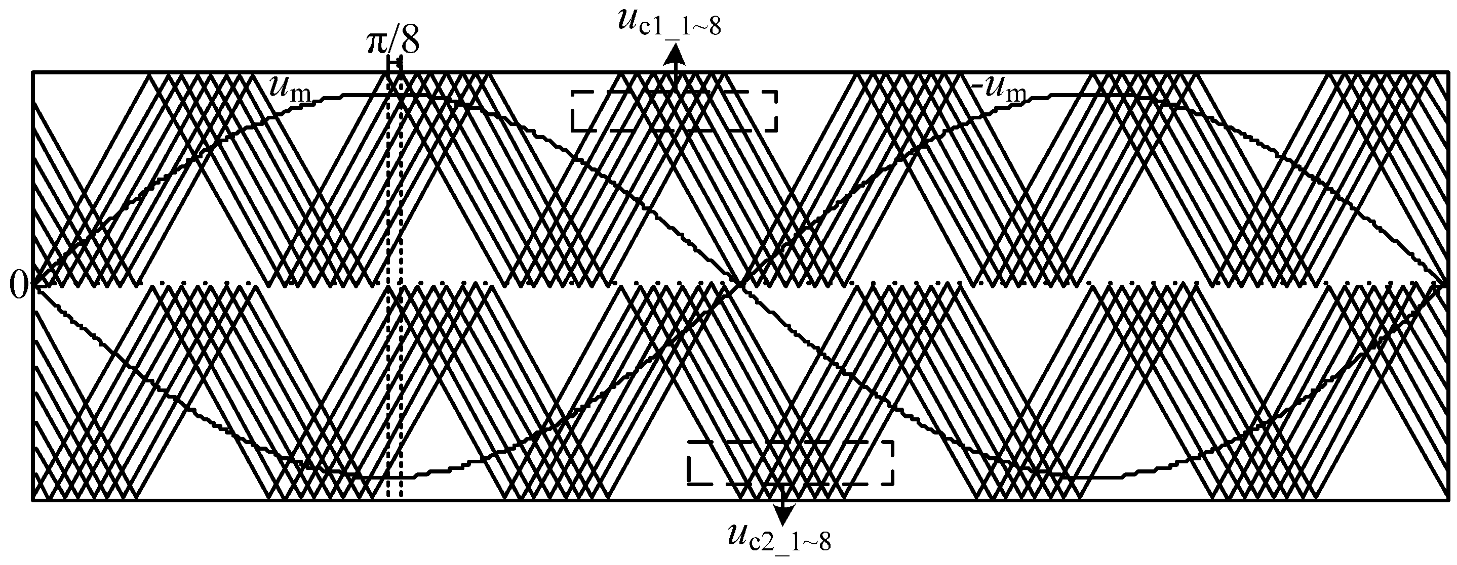
The schematic of PSC-SPWM used in cascade inverters is shown in
Figure 6. The Fourier fundamental of the output voltage of an H-bridge is:
In Equation (1),
Jk is on behalf of the
k-th Bessel function and
vdc is the DC voltage. Besides,
vo represents the output voltage of the inverter.
Figure 6.
Phase shift carrier schematic.
Figure 6.
Phase shift carrier schematic.
In Equation (2), θ
k (
k = 1, 2, 3…
N) is phase shift angle. The increasing angle of each H-bridge is θ
k = π/
N (
N is the number of H-bridge):
In Equation (3), there is n = 2, 4, 6 …, B = 0 and when n < 2N, the A = 0 is established. As can be seen from the above derivation, the total output voltage of the H-bridge is the algebraic sum of the basic units. Cascade inverters can be equivalent to a high single carrier frequency converter. The equivalent frequency is 2N times as the frequency of the carrier. In conclusion, PSC-SPWM can be implemented equivalent to the function of higher switching frequency with low power switching devices so that the switching loss can be reduced.
2.3. DC-Link for the Three-Phase to Single-Phase Converter
When the multilevel diode clamped converter transfers active power, the DC capacitor voltage will become unbalanced. To solve the problem of DC capacitor voltage unbalance, an inductive auxiliary circuit is added to this paper on the DC-link [
18].
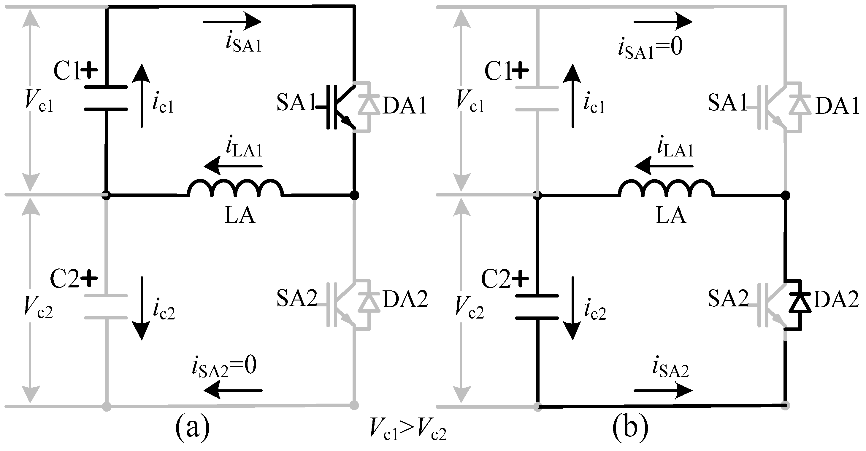
The diagram of the inductance equalizing circuit is shown in
Figure 7. The specific control principle is as follows: when
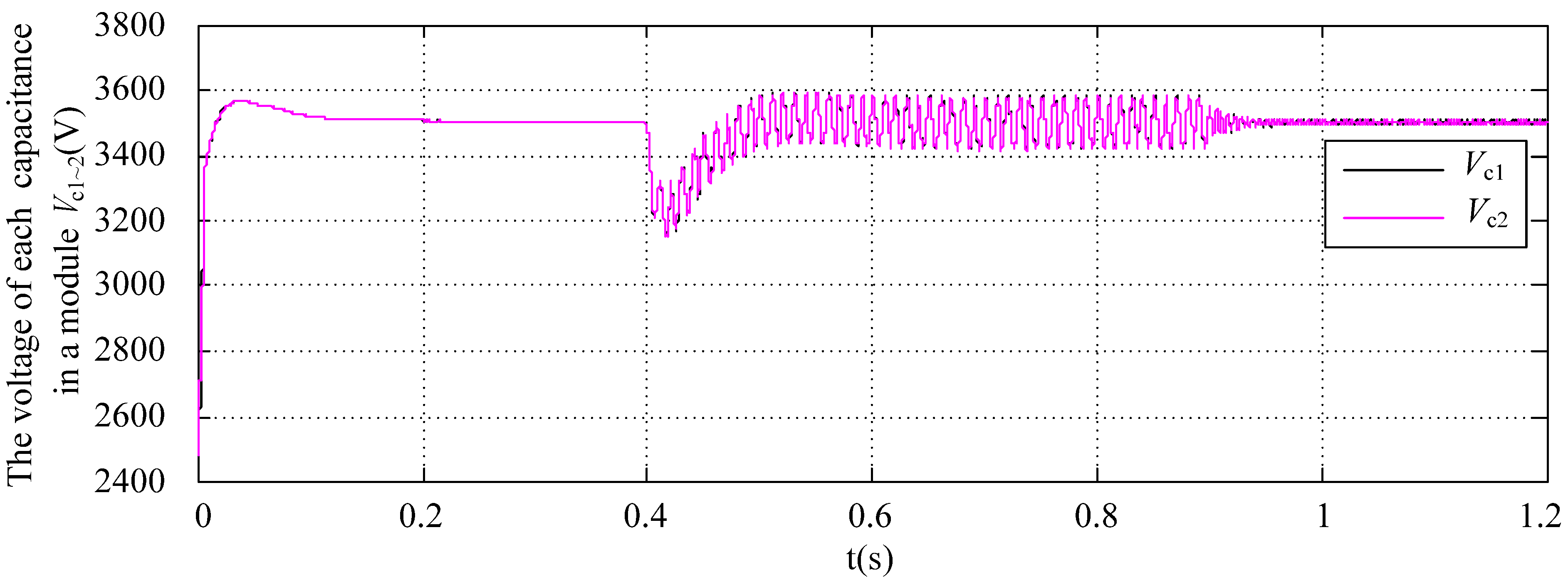
Vc1 is larger than
Vc2, SA1 turns on while SA2 is off, then the capacitor C1 will be discharged with the inductance LA. The capacitor’s voltage
Vc1 decreases, and the inductance’s current increases. Since the energy stored in C1 is delivered to LA via the path shown in
Figure 7a, the voltage
Vc1 decreases and
Vc2 remains unchanged. Meanwhile, the discharge current
iLA1 will increase linearly from zero. Secondly, SA1 is turned off, and SA2 also maintains an off state. The anti-parallel diode DA2 provides a discharge path for LA as shown in
Figure 7b. The energy stored in LA will be delivered to C2. Therefore
Vc2 increases, whereas
Vc1 remains unchanged. This stage will be ended once
iLA1 reaches zero. The process will not end up until
Vc1 =
Vc2. On the contrary, if
Vc1 <
Vc2, the process is just the opposite.
Figure 7.
The inductance equalizing circuit of 3L-NPC. (a) Discharge current path from C1 to LA at VC1 > VC2 stage 1; (b) Charge current path from LA to C2 at VC1 > VC2 stage 2.
Figure 7.
The inductance equalizing circuit of 3L-NPC. (a) Discharge current path from C1 to LA at VC1 > VC2 stage 1; (b) Charge current path from LA to C2 at VC1 > VC2 stage 2.
As is well known, a double line-frequency ripple of DC voltage would appear on the DC-link [
19]. In this paper, a LC filter circuit is designed to eliminate the double line-frequency ripple:
where,
idc2 is the twice grid-frequency current,
Vt and
It are the voltage and current of cascade inverter output, respectively.
Vdc is the DC-link voltage of each three-phase to single-phase converter, ω
0 is angular frequency, φ is the power factor angle of the load. When the circuit is under resonant state,
idc2 flow through the LC filter circuit. Therefore, the capacitor’s voltage
vc of the LC filter is shown in Equation (5):
Generally, the amplitude of
vc is less than 10% of DC-link voltage. So the L (inductor) and C (capacitor) is designed in Equations (6) and (7):


