Article

Design of an LLC Resonant Converter for Driving Multiple LED Lights Using Current Balancing of Capacitor and Transformer

1
LG Innotek Co., Ltd., 26, Hanamsandan 5beon-ro, Gwangsan-gu, Gwangju 506-731, Korea
2
Department of Electrical Engineering, Chonnam National University, Gwangju 500-757, Korea
*
Author to whom correspondence should be addressed.
Energies 2015, 8(3), 2125-2144; https://doi.org/10.3390/en8032125
Submission received: 3 November 2014 / Accepted: 12 March 2015 / Published: 18 March 2015

Abstract

:
In this study, to achieve the constant current drive and brightness control without a separate pulse width modulation (PWM) converter, a single converter is designed and verified by experiment under the condition of a multiple LED light load with different output voltage (Vf) characteristics. In the case of the input of 140 Watt class level, the proposed converter can drive two voltage type 95 Vdc (300 mA) light emitting diode (LED) lights loads and 120 Vdc (300 mA) LED lights loads simultaneously. In addition, to improve commercial compatibility, the proposed converter is operated in a wide range of the input voltage 90~264 Vac; also, the Power Factor Correction (PFC) circuit with the input power factor of more than 0.9 is added. In order to maximize the power conversion efficiency, a LLC resonant converter is applied to the PFC block with the output voltage of 380 Vdc and to a DC-DC conversion block. Finally, reliability of the proposed converter is verified through total harmonic distortion (THD) and electromagnetic interference (EMI) tests.

1. Introduction

Recently, the topic of “low-carbon green growth industry” has been actively researched and developed. Especially, the renewable energy and carbon dioxide emission market has been rapidly expanding due to climate change and the energy crisis. Energy savings are required in order to reduce the carbon dioxide that causes the green-house effect. The total global power consumption of lighting is 2 trillion, 100 billion kWh, which is 12%~15% of the global annual power consumption. 1.7 billion tons of carbon oxide is emitted annually according to the power consumption of lighting. For this reason, research into highly efficient lights has been actively carried out. A Light Emitting Diode (LED) has high luminous efficiency and 20%~30% power savings compared to a conventional light source. Annually 250 billion kWh power and 150 million tons of carbon oxide could be reduced through the use of LED lights [1,2].
The LED is turned on when the applied voltage is more than the forward voltage, a LED is a diode. To modify the variable lighting characteristics, multi LEDs can be composed as a series array or parallel string. For the design of an LED converter, consideration of LED forward voltage variation (±5%~10%) is required [3,4,5,6,7,8].
Figure 1 shows a simplified LED driving circuit with a multi-string structure. Since the currents differ between each channel according to the impedance, a large current can be injected into one channel of low impedance and can reduce the life time of the LEDs, leading to their destruction [9,10]. Recently, to achieve LEDs with high luminous efficiency, multi LEDs are used in a single luminary structure. In the case of multi-string lighting, each LED string has a different impedance. Because all the LEDs (Vf) have different voltages, an individual boost or buck PWM converter is needed for each LED. In addition, in the case of outdoor lights such as street lights and security lights, variable brightness is needed according to the lighting conditions and a multi LED driver is required [11,12,13]. However, when applying individual converters to each LED, the system cost is increased and the efficiency and life time of the system are reduced.
Figure 1. Simplified LED driving circuit with multi-string structure.
Energies 08 02125 g001
In this paper, an LLC resonant converter for driving multiple LED lights using the current balancing of a capacitor and transformer is proposed. The proposed converter can drive multi LED strings without an individual converter with constant current control and dimming control. To improve the compatibility of the product, the proposed converter is designed with a wide input voltage range of 90~264 Vac and high power factor (over 0.9). Furthermore, to maximize the efficiency, a DC/DC block is designed as an LLC converter. A THD and an EMI noise tests are performed to verify the reliability of the proposed converter.

2. Converter for Driving LED Lights

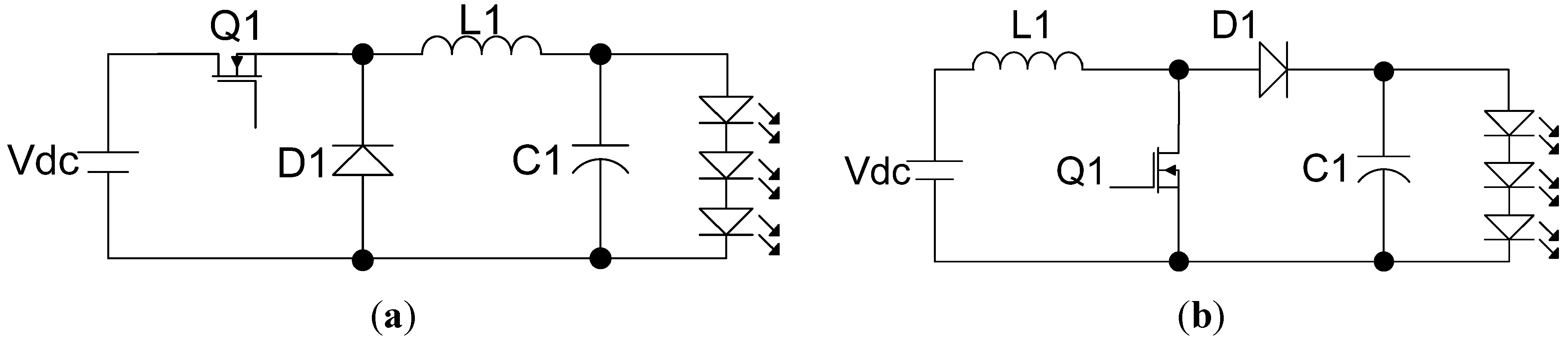
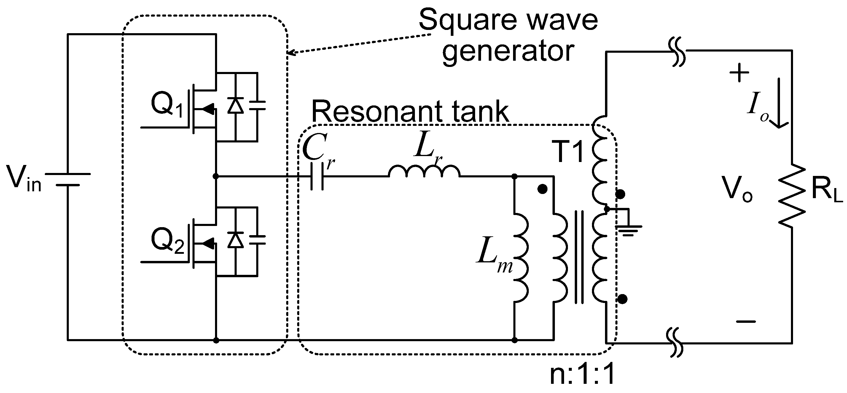
2.1. Conventional Converter for LED Application

Figure 2 shows a conventional converter type for high power LED lighting power. The system consists of an AC power input part and a PFC circuit for improving the power factor, a DC/DC converter for building output voltage, and an LED driver for providing a constant current to the LED load. A fly-back and LLC resonance converter are usually used for the DC/DC converter [14,15,16,17].
Figure 2. Conventional LED driving circuit.
Energies 08 02125 g002
Figure 3a shows a buck DC/DC converter mostly used for constant LED current control. The buck converter can be adapted in the case of an LED voltage lower than the input voltage, and requires a duty ratio of less than 85%. The output voltage is controlled by the MOSFET’s on/off operation through the charge and discharge of an inductor current.
Figure 3b shows a boost DC/DC converter which is used when the LED voltage is higher than the input voltage. The converter can achieve 90% upper efficiency and has an advantage in EMI due to the filter effect of the main inductance [18].
Figure 3. Buck and Boost converter for LED Application. (a) buck converter; (b) boost converter.
Energies 08 02125 g003

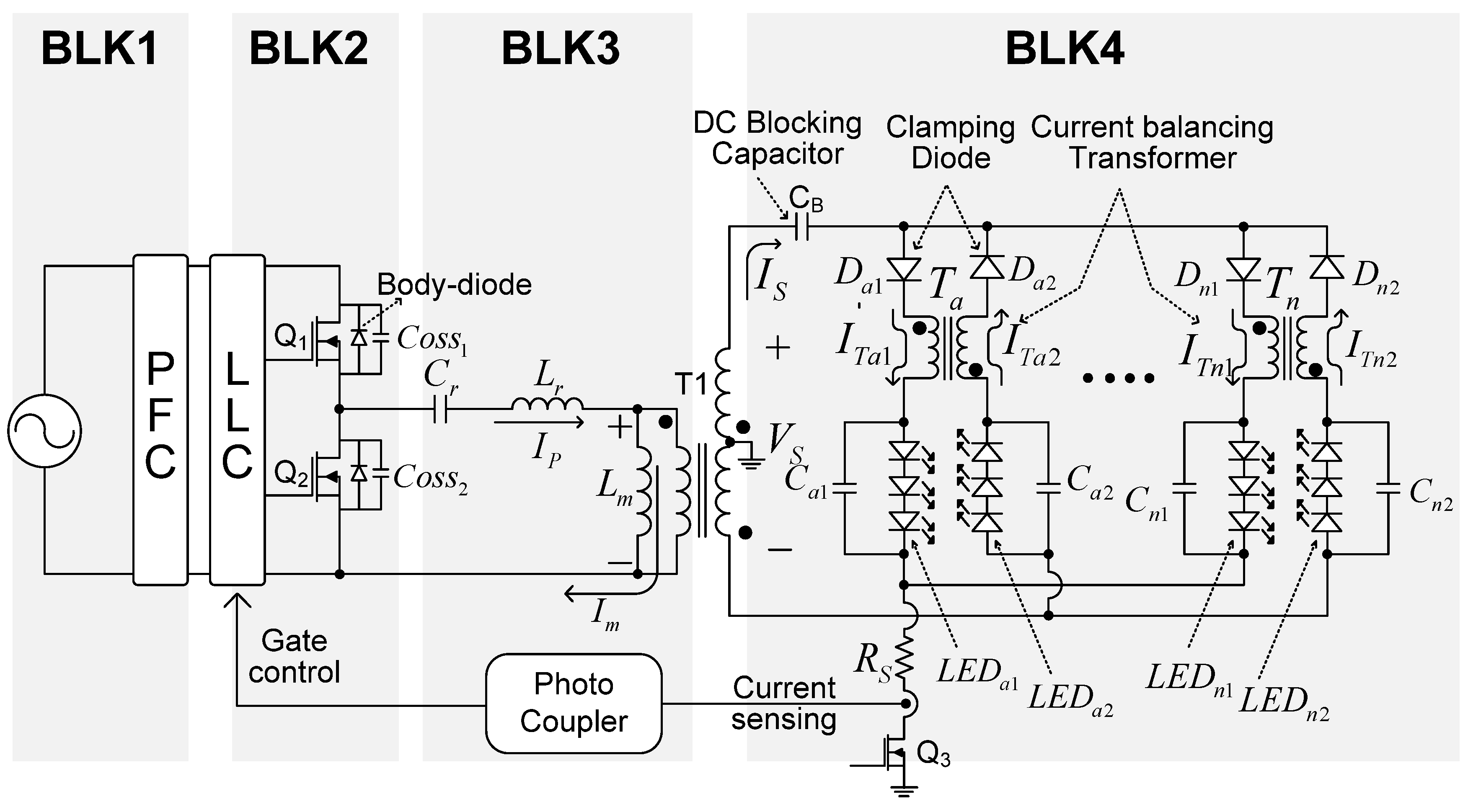
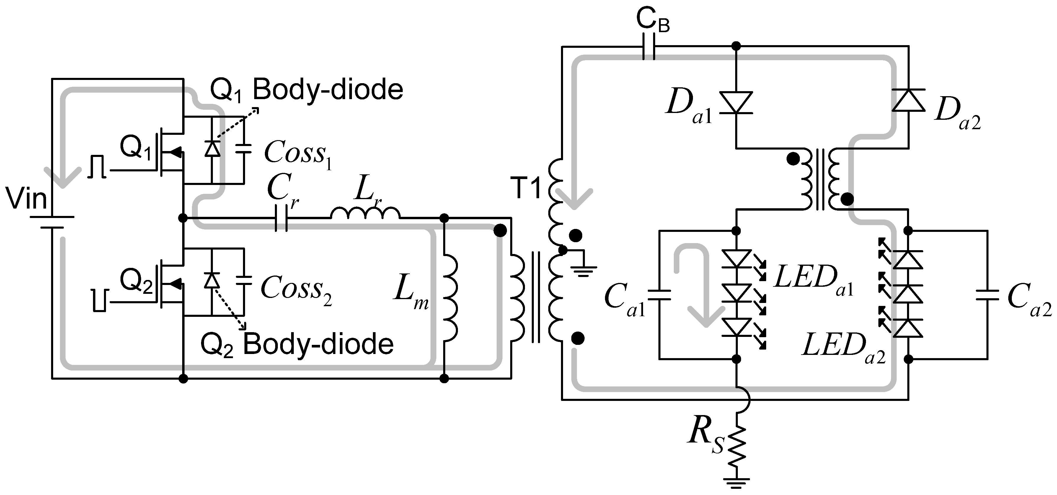
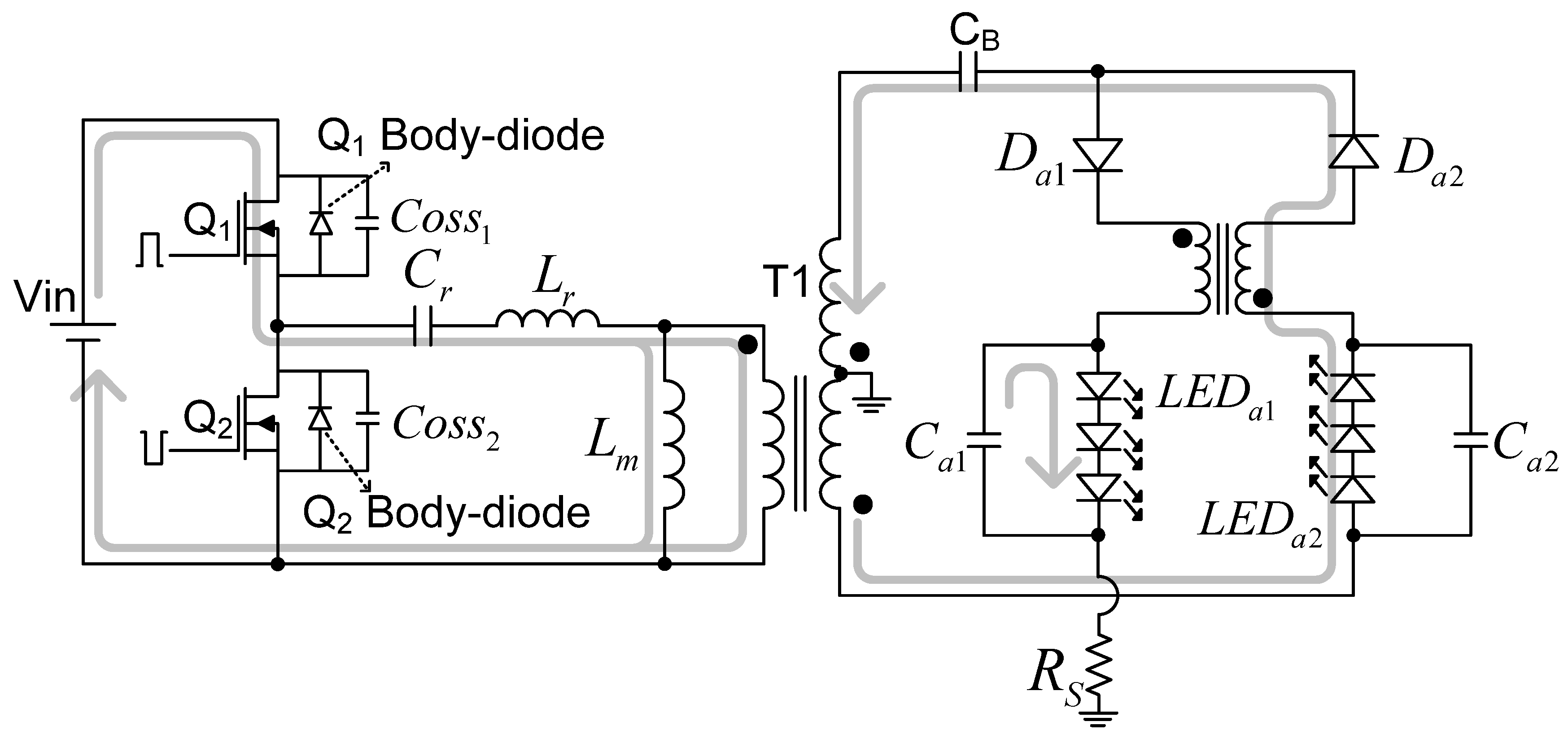
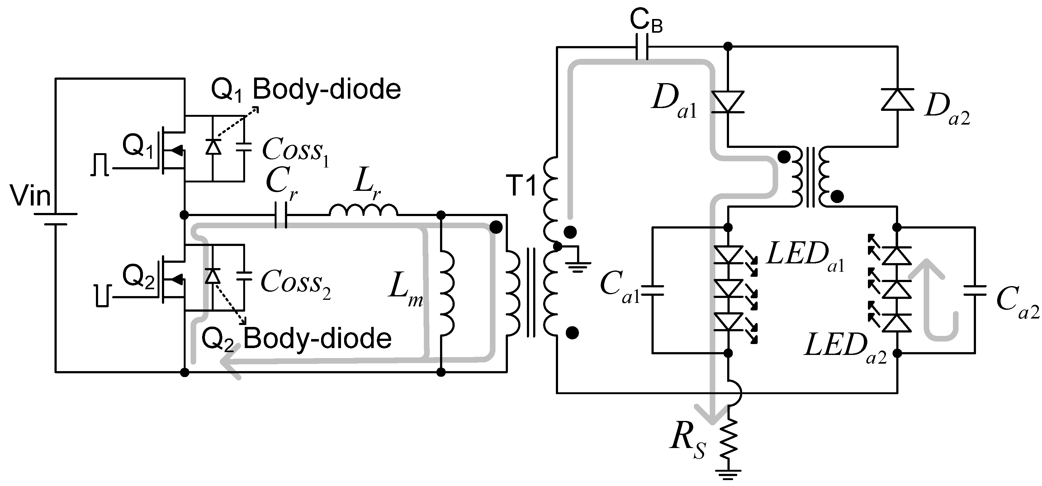
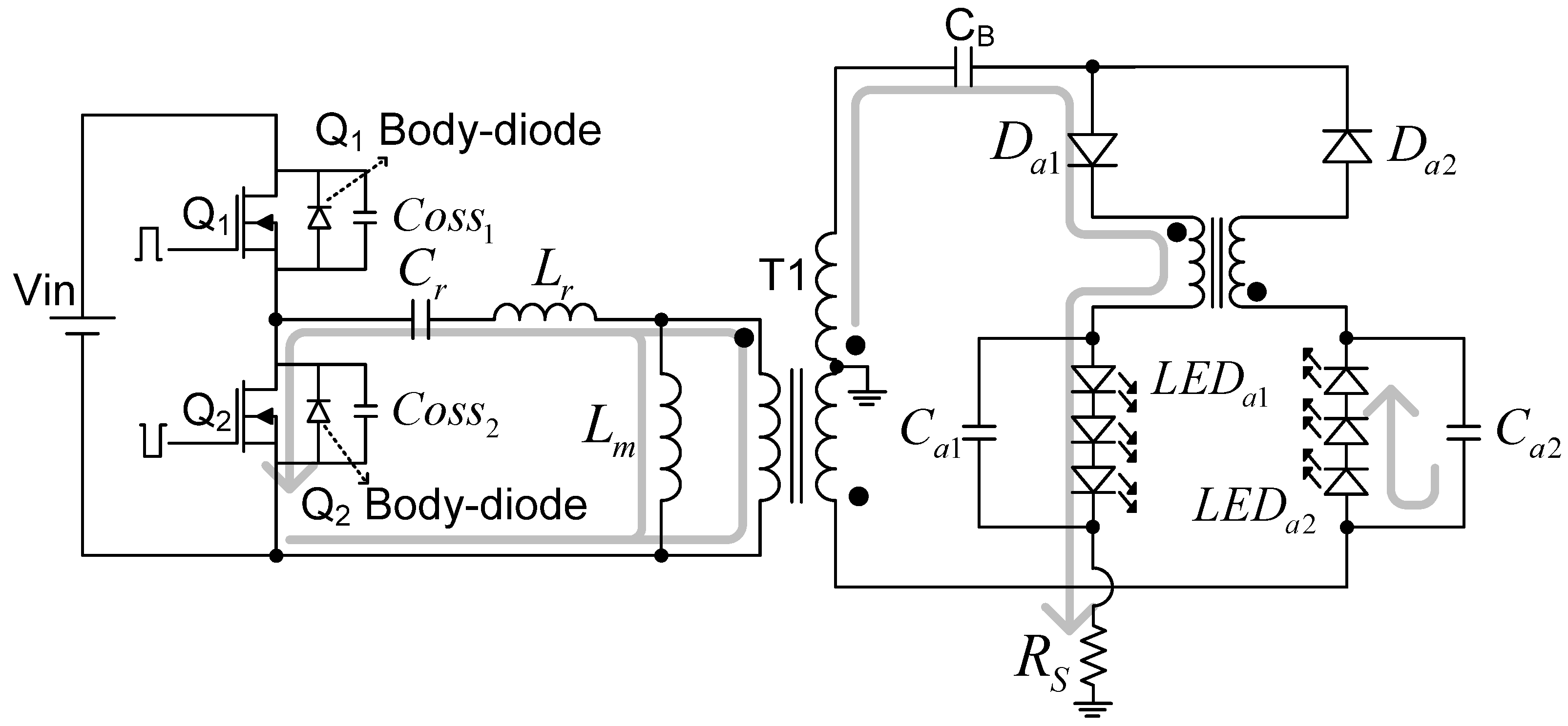
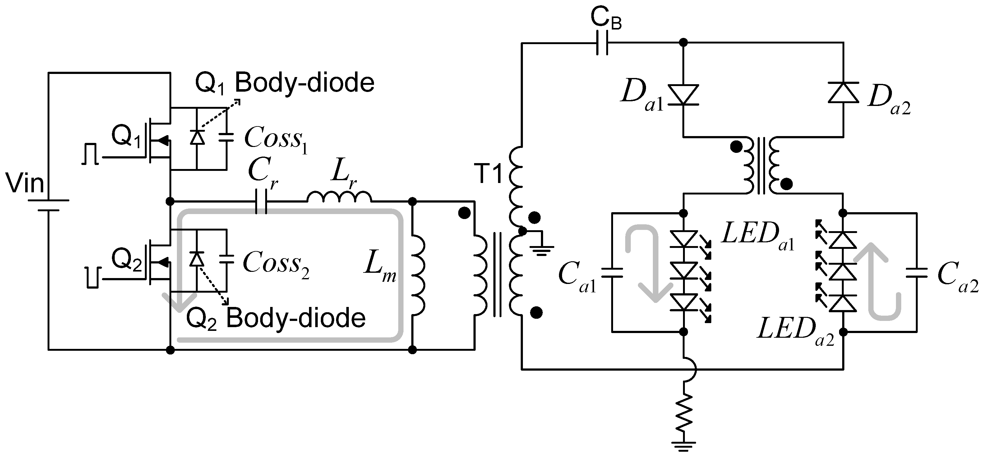
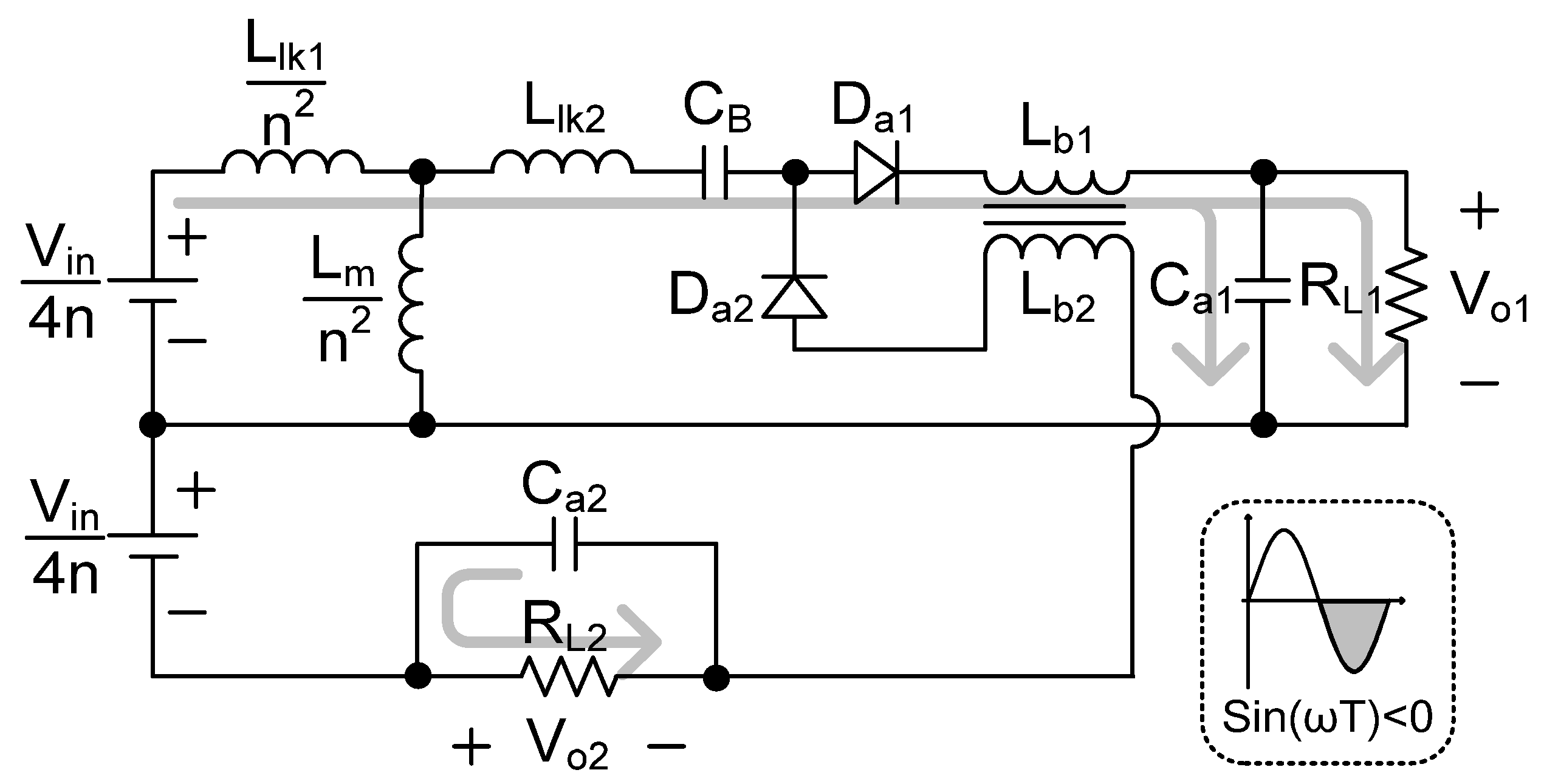
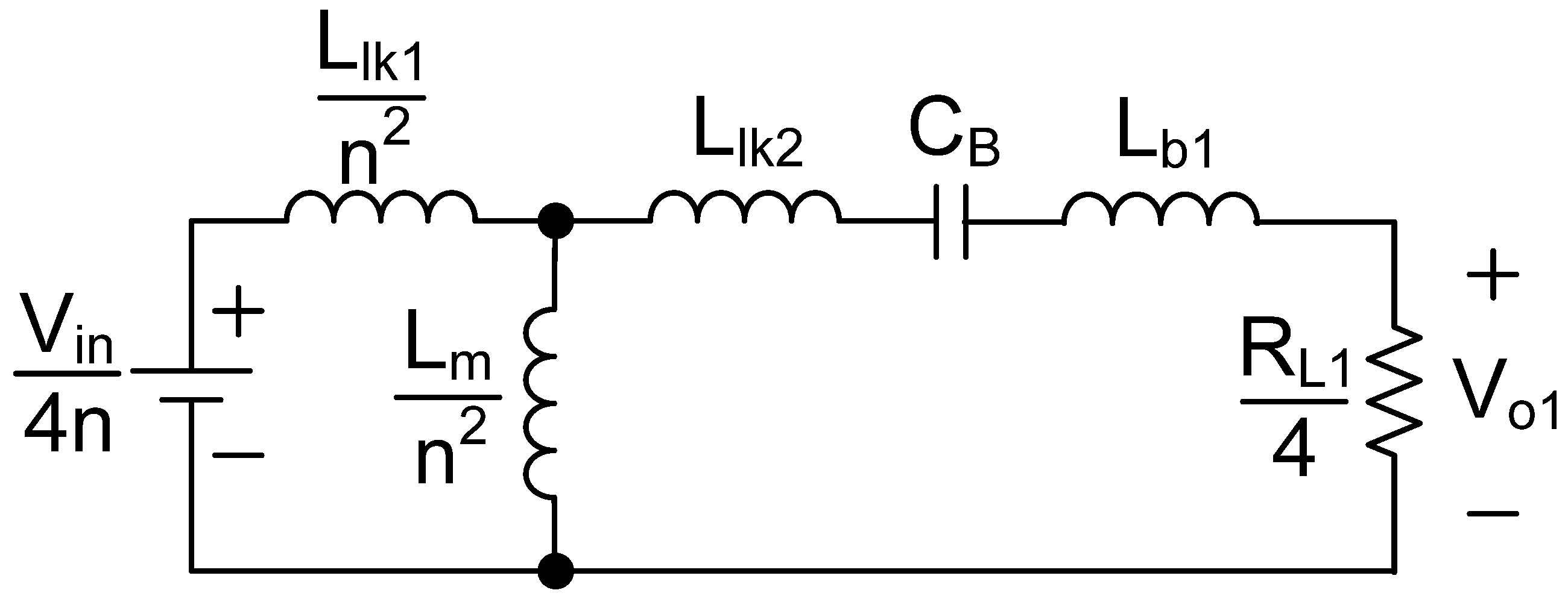
2.2. Proposed Current Balancing Converter for Driving LED Lights
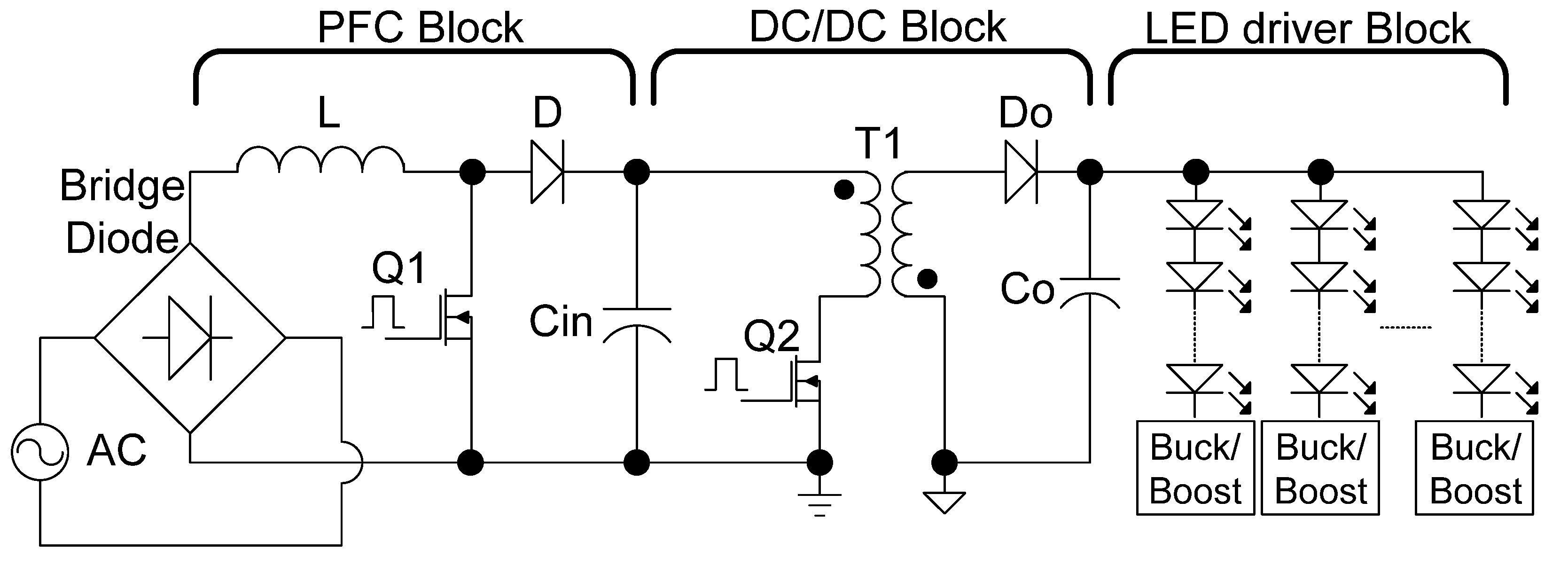
Usually, a high switching frequency is required to reduce the size of the converter, but this causes an increase of switching loss in a hard switching mode.
In this paper, an LLC resonance converter with Zero Voltage Switching (ZVS) operation is proposed. The proposed converter using high frequency and ZVS is adapted to reduce switching loss. Figure 4 shows the schematic of the proposed converter. As shown, a DC blocking capacitor, clamping diode, and current balancing transformer are used instead of the switching regulator in the second stage of the converter.
Figure 4. Proposed current balancing converter.
Energies 08 02125 g004
Proposed multi LED lights drive converter consists of four blocks.
BLK1
A PFC block for achieving high power factor with wide input voltage range from 90 Vac to 264 Vac.
BLK2
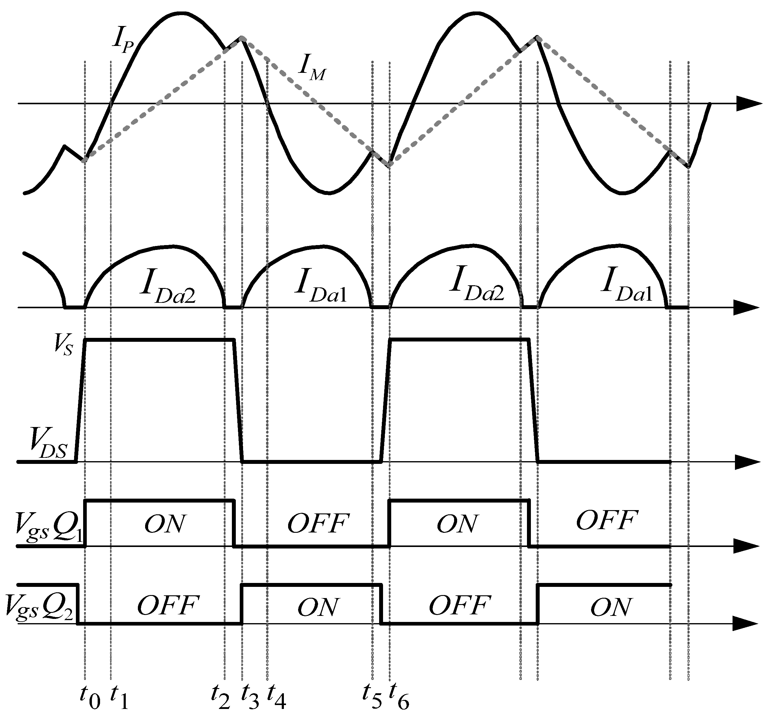
A half bridge block makes a square wave voltage with 380 Vdc input and nearly 50% duty ratio. The block has a short dead time to ensure continuous current flow.
BLK3
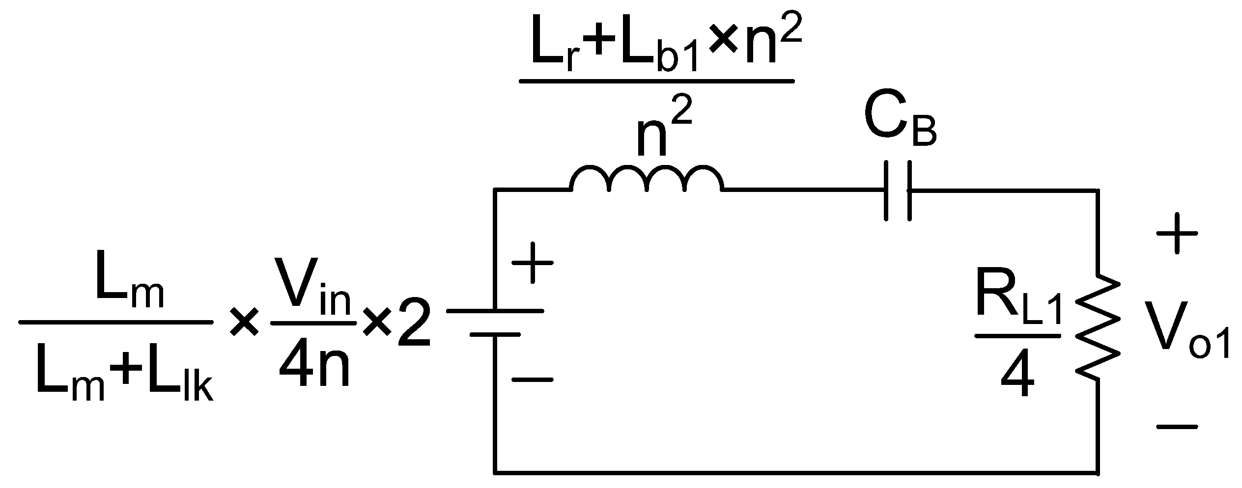
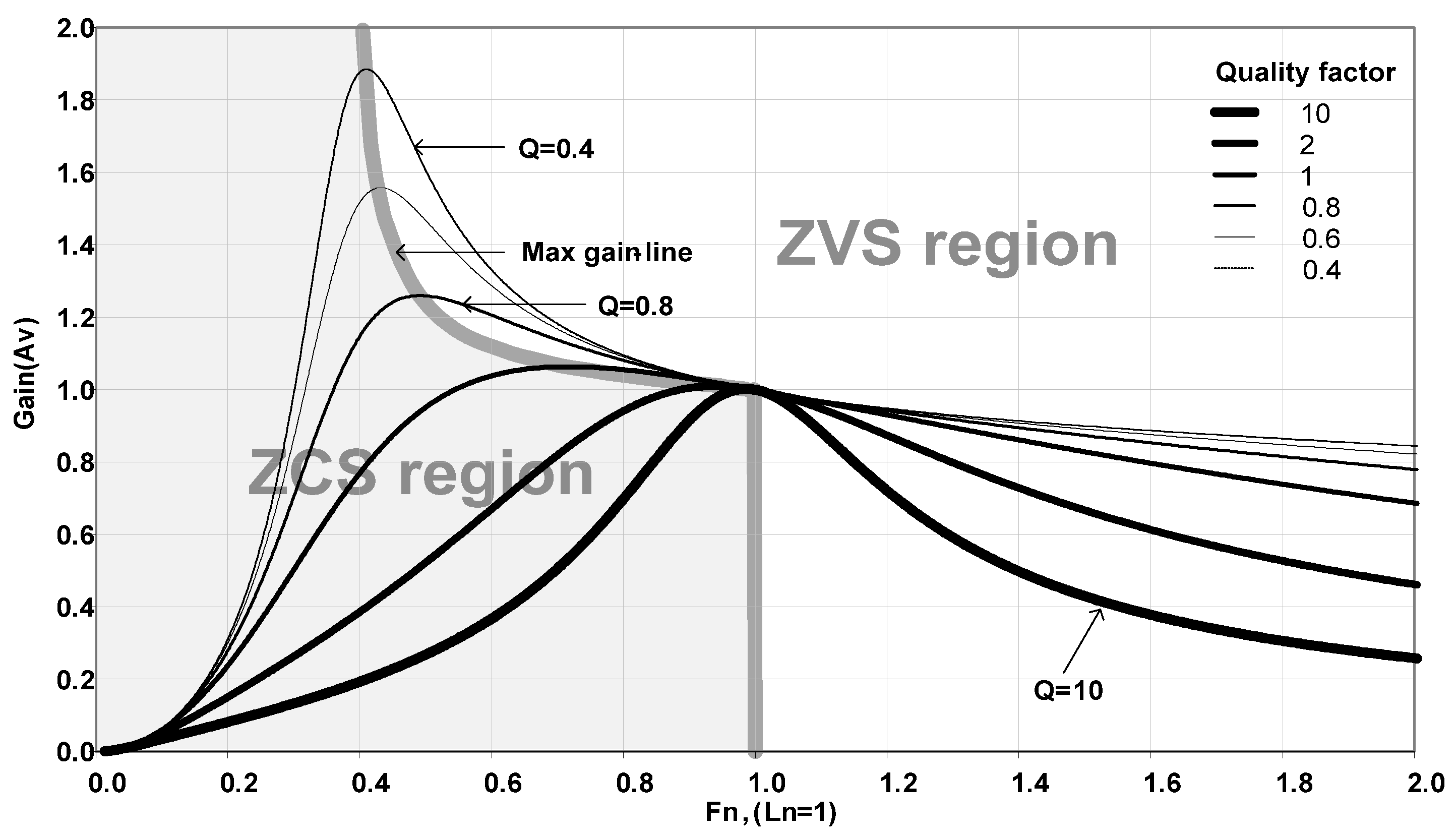
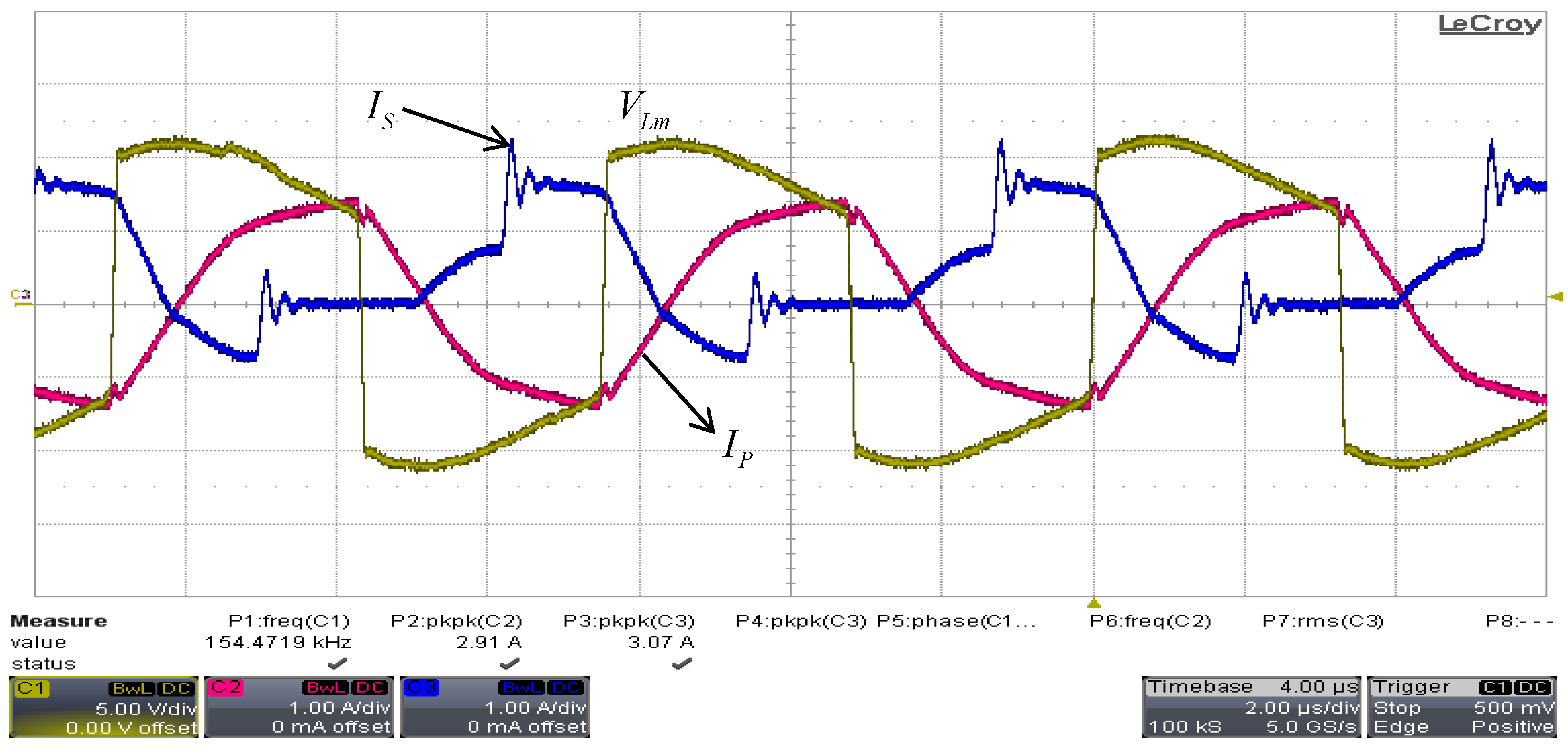
A resonant tank block consisting of a capacitor C r and magnetizing inductance of transformer L m . The resonance tank operates with high frequency and creates a sinusoidal current from the square wave voltage from BLK2. Since the primary current I P is delayed by resonance, MOSFET is turned on with the ZVS condition.
BLK4
A resistor R S of this block is used for LED current sensing and limiting. A regulated DC voltage is applied to an LED load through D a 1 ( D n 1 ) and D a 2 ( D n 2 ). C a 1 ( C n 1 ) and C a 2 ( C n 2 ) are connected parallel to the LED load and the DC voltage is made smooth. The larger capacitance can further reduce AC noise.
A capacitor C B allows only an AC signal to pass. At the first half cycle of AC signal, the capacitor C B compensates the voltage differences of each channel and drives a high voltage channel. At the other half cycle of the AC signal, the capacitor C B removes the offset voltage and drives a low voltage channel. Thus, during a single period ( T S ), the capacitor charges/discharges the total energy and the change of voltage is zero. This can be expressed by Equation (1). Based on Equations (1) and (2), the voltage change of the capacitor C B is calculated as zero, which is a basic principle of a capacitor volt-sec balance equation:
V C B = ( t + T S ) V C B ( t ) = 1 C t t + T s i C B d t
0 = 1 T s t t + T s i C B ( t ) d t
Since the balancing transformers are operating under AC excitation, the following Equation (3):
N T a 1 × i T a 1 = N T a 2 × i T a 2 … … N T n 1 × i T n 1 = N T n 2 × i T n 2
Primary turns and primary current respectively of the balancing transformer. N T n K and i T n K denote the secondary turns and secondary current respectively of the Kth balancing transformer.
Since with the loop connection the secondary winding current is equalized as follows:
i T a 1 = i T a 2 = i T n K
And this further results in:
i T a 1 = ( N T a 2 / N T a 1 ) × i T a 2
In this paper current balancing transformer T a ( T n ) for constant current control has a 1:1 winding ratio according to equation N T a 1 × i T a 1 = N T a 2 × i T a 2 and the same current flows at L E D a 1 ( L E D n 1 ) and L E D a 2 ( L E D n 2 ). The current which flows though transformer Ta can be expressed by Equation (6):
i T a 1 = i T a 2 = i L E D
The voltage across the second side of transformer T 1 can be expressed by Equation (7):
V s = 1 2 ( v C B v D a 1 v T a 1 + v L E D a 1 + v R s ) = v C B + v D a 2 + v T a 2 + v L E D a 2
Figure 5 shows the current and voltage waveforms according to the operation mode of the LLC resonant converter.
Mode 1 ( t 0 to t 1 ): At t 0 , Q 1 is on state and Q 2 is off state. The switch current I P flows through the body diode of MOSFET Q 1 by C r , and the L r resonance and a voltage across the MOSFET Q 1 is zero. A voltage of C o s s 2 which is connected to the MOSFET Q 2 drain-source is charged to the Vin level. An output current then starts to flow through diode D a 2 (Figure 6).
Figure 5. Operation waveform of LLC resonant converter.
Energies 08 02125 g005
Figure 6. Circuit diagram during Mode 1.
Energies 08 02125 g006
Mode 2 ( t 1 to t 2 ): A Q 1 is in the turn-on state and inductor current I P flows in the positive direction. An input voltage is applied to a transformer and current ( I m ) of the magnetizing inductance ( L m ) increases linearly (Figure 7).
Figure 7. Circuit diagram during Mode 2.
Energies 08 02125 g007
Mode 3 ( t 2 to t 3 ): At the t 2 , Q 1 is in the turn-on state and Q 2 is in the turn-off state. Inductor currents I P and I m have the same value and the output current is zero. The current I m begins to charge C o s s 1 of Q 1 . At the same time, C o s s 2 of Q 2 discharges by I m . Charged capacitors that are connected parallel to each LED supply the energy to the LED loads (Figure 8).
Figure 8. Circuit diagram during Mode 3.
Energies 08 02125 g008
Mode 4 ( t 3 to t 4 ): Q 1 is in the turn-off state and Q 2 is in the turn-on state. The current I P flows through the Q 2 body diode and the voltage across the Q 2 becomes zero (ZVS Condition). An output current flows to the LED load through capacitor C B and diode D a 1 . D a 2 is in reverse bias with no current flowing through (Figure 9).
Mode 5 ( t 4 to t 5 ): An opposite mode to Mode 2. In this mode, a half AC voltage according to the center tap of the transformer is applied to an LED through D a 1 (Figure 10).
Figure 9. Circuit diagram during Mode 4.
Energies 08 02125 g009
Figure 10. Circuit diagram during Mode 5.
Energies 08 02125 g010
Mode 6 ( t 5 to t 6 ): An opposite mode to Mode 3. In this mode, a half AC voltage from the center tap of the transformer is applied to an LED through D a 1 (Figure 11).
Figure 11. Circuit diagram during Mode 6.
Energies 08 02125 g011
Figure 12 shows an equivalent circuit for the primary side of the LLC resonant converter. A square wave generator block and resonant tank block are in this circuit.
Figure 12. Equivalent circuit of primary side converter.
Energies 08 02125 g012
Resonant frequency and transformer turn ratio can be expressed by Equations (8) and (9):
f 0 = 1 2 π L r C r
n = V i n / 2 V 0
An LLC converter can be described using fundamental approximation. Figure 13 shows a fundamentally approximated circuit according to the ac input for the primary side of the LLC resonant converter. Load voltage V o a , load current I o a , and load resistance R o a can be expressed by Equations (10)–(12). Equation (13) expresses the gain characteristics and Equations (14) and (15) express the Quality Factor.
Figure 13. Fundamental approximated circuit of primary side.
Energies 08 02125 g013
V o a = 2 2 π n V 0
I o a = ( π 2 2 I o ) / n
R o a = 8 n 2 R L π
A v = n V o V i n / 2 = | j ω L m R o a j ω L m + R o a j ω L m R o a j ω L m + R o a + 1 j ω C r + j ω L r | = | L n f a 2 L n f n 2 + ( f n 2 1 ) ( 1 + j f a L a Q ) |
Q = L r / C r R o a , f a = f min f o , L a = L m L r
f min = 1 2 π C r ( L r + L m )
Figure 14 shows the operation classification of the LLC converter. The operation of an LLC converter can be classified into 3 regions according to switching frequency. In the case whereby the phase of input voltage (Vac) precedes the phase of I P , it can be expressed as the zero current switching (ZCS) operation region.
Figure 14. Operating region of LLC resonant converter.
Energies 08 02125 g014
Figure 15 shows the gain characteristics of an LLC resonant converter in the condition of L n ( L m / L r ) = 1 . The operation mode is classified as within the ZVS region with high switching frequency and the ZCS region, with low switching frequency relative to resonant frequency. An LLC converter is usually used with a ZVS condition because in the case of a ZCS condition, a high current is injected when the switch is on, which destroys the MOSFET. If the maximum gain point is required to move left or a balanced gain characteristic is required, enlarging L n can be useful.
Figure 16 shows the Mode 2 operation in the equivalent circuit of the converter’s secondary side. A primary side transformer is converted to inductance in the equivalent circuit. L m is mutual inductance, while L l k 1 and L l k 2 are the leakage inductance of transformer at the primary and secondary side, respectively. R L 1 and R L 2 are converted values of the LED load. The input voltage is twice the center tap voltage V i n / 4 n × 2 , thus R L 2 is more appropriate for a high voltage LED load than R L 1 . An output current flows through C B by D a 2 and L b 2 . A charged energy in the C a 1 discharges to R L 1 .
Figure 15. Gain characteristics of LLC resonant converter.
Energies 08 02125 g015
Figure 16. Equivalent circuit of secondary side converter (Sinωt > 0).
Energies 08 02125 g016
Figure 17 shows the Mode 5 operation. The input voltage is twice center tap voltage V i n / 4 n , thus R L 1 is more appropriate for use with a high voltage LED load than R L 2 .
Figure 17. Equivalent circuit of secondary side converter (Sinωt < 0).
Energies 08 02125 g017
Figure 18 shows the simply modified equivalent circuit of Figure 17. The load voltage is V o / 2 and the load current is 2 I o , and the LED load can then be expressed by R L 1 / 4 .
Figure 18. Simplified equivalent circuit of secondary side converter.
Energies 08 02125 g018
Figure 19 shows a simplified equivalent circuit compared to that of Figure 18, relative to voltage gain.
Figure 19. Simplified equivalent circuit of secondary side converter.
Energies 08 02125 g019
The voltage gain in a negative region can be expressed by Equation (16) and the voltage gain according to switching frequency can be found by this equation. Equation (17) shows the voltage gain in a positive region:
V o V i n = L m L m + L l k × 4 n × 2 × R L 1 4 ( ω L r + L b 1 × n 2 n 2 1 ω C B ) 2 + ( R L 1 4 ) 2
V o V i n = L m L m + L l k × 2 n × 2 × R L 2 4 ( ω L r + L b 2 × n 2 n 2 1 ω C B ) 2 + ( R L 2 2 ) 2
The transformer requires design according to the high voltage load and the turn ratio is determined using Equation (18):
n = N P N S = V S 2 ( V L E D + V D a 2 ) = 380 V 2 ( 120 V + 1.2 V ) 1.5
An equivalent resistive value of the LED load is expressed by Equation (19):
R e q = 8 n 2 π 2 V o 2 P o = 8 × 1.5 2 3.14 2 120 2 129 203 Ω
The resonant component C r can be determined from Equation (20). An equation of Q factor is ( L r / C r ) / R e q and 0.4~0.5 is the ideal value. The Q factor of the proposed converter is determined to be 0.45 and the resonant frequency is determined to be 85 kHz. For the experiments, two 10 nF capacitors are adapted with parallel connection:
C r = 1 2 π Q × f o × R e q ( Q 0.45 , f o 85 k H z ) = 1 2 × 3.14 × 0.45 × 85 × 10 3 × 203 20 n F
The resonant component L r can be determined from Equation (21) and 220 μH is selected in the proposed converter according to the transformer bobbin and winding limitation:
L r = 1 ( 2 π f o ) 2 C r = 1 ( 2 × 3.14 × 85 k H z ) 2 × 20 n F 175 μ H
The primary side inductance L P is expressed in Equation (22). The L k is a ration of the mutual inductance to the primary side leakage inductance. Usually, 3 to 8 is used for the L k value and 6 is selected for the proposed converter. The L P is calculated as 659 μH from Equation (22) and 650 μH is applied for the experiments:
L P = ( k + 1 ) 2 ( 2 k + 1 ) L r = ( 6 + 1 ) 2 ( 2 × 6 + 1 ) × ( 175 × 10 6 ) 659 μ H   ( L k = L m / L l k )

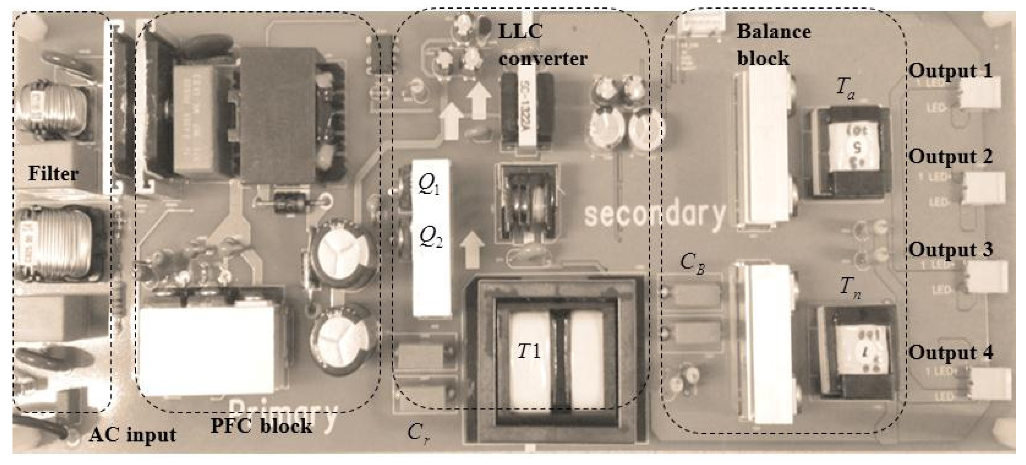
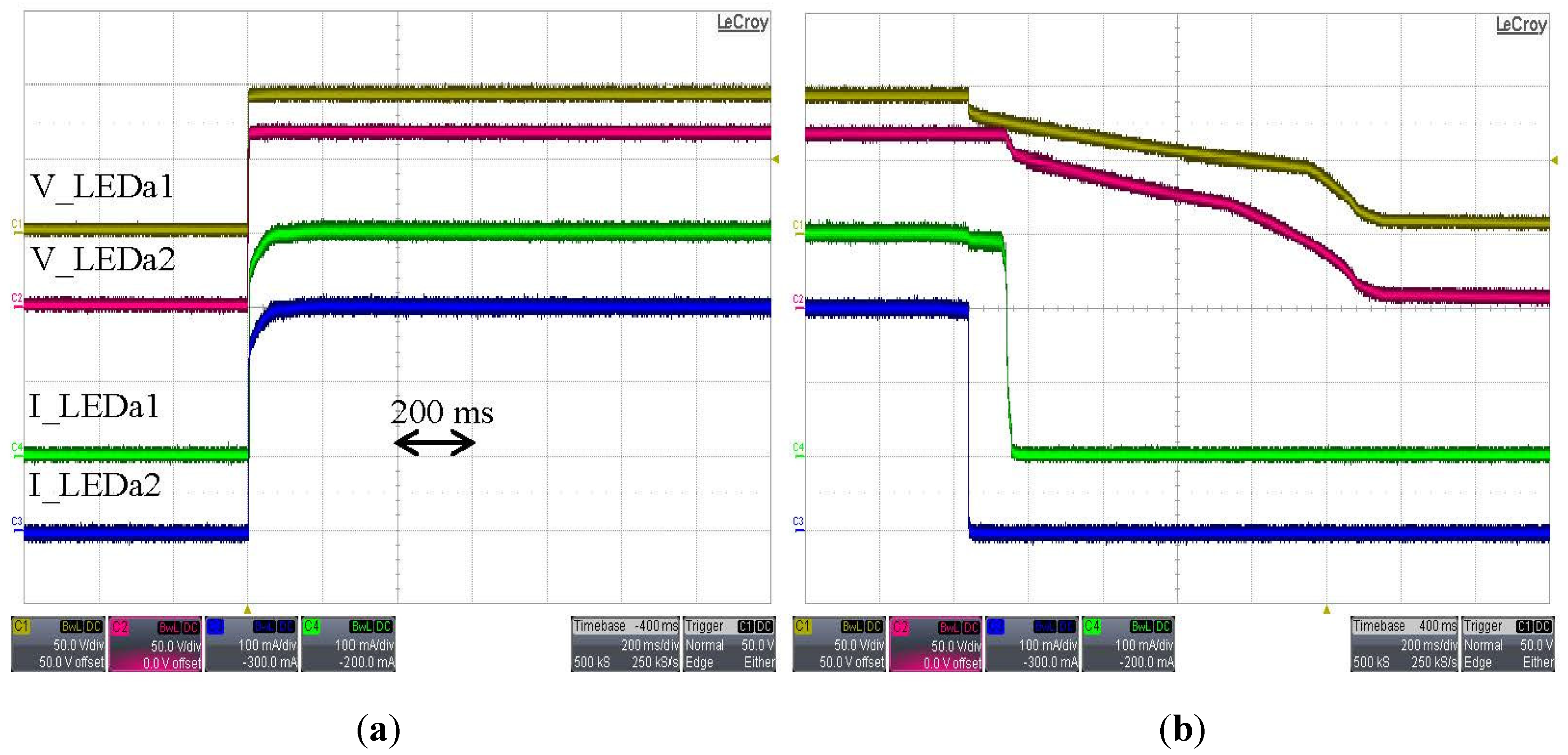
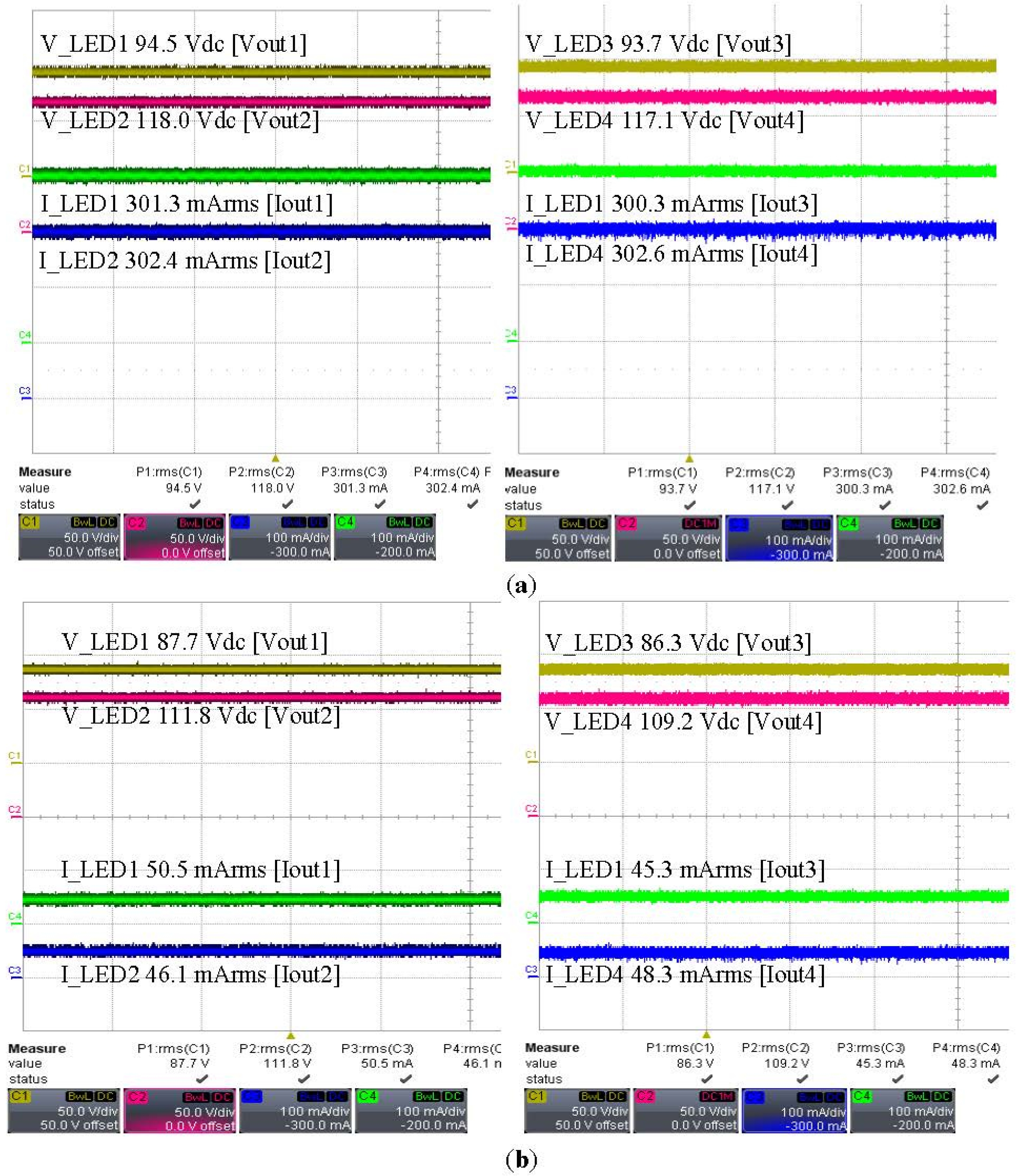
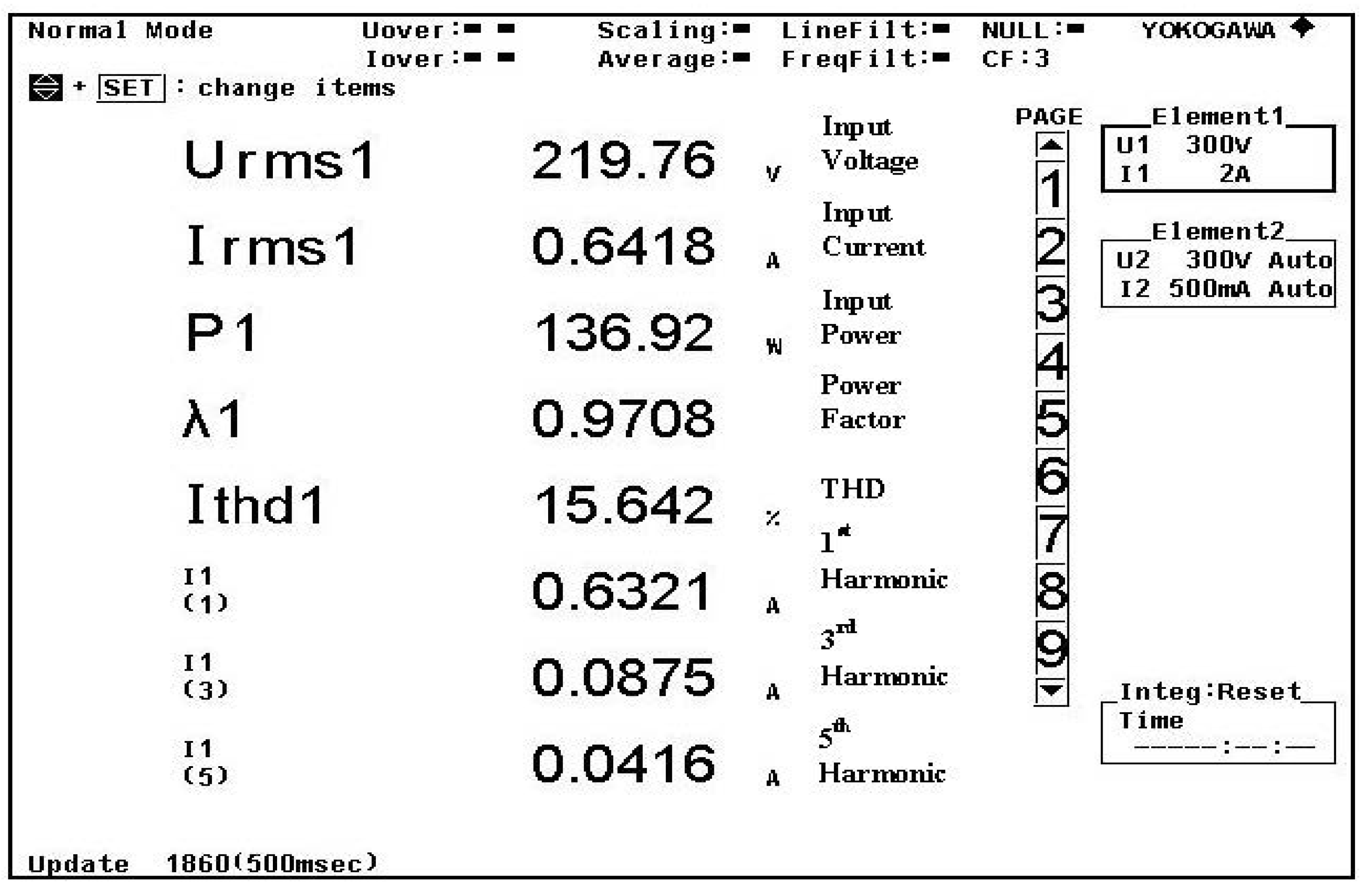
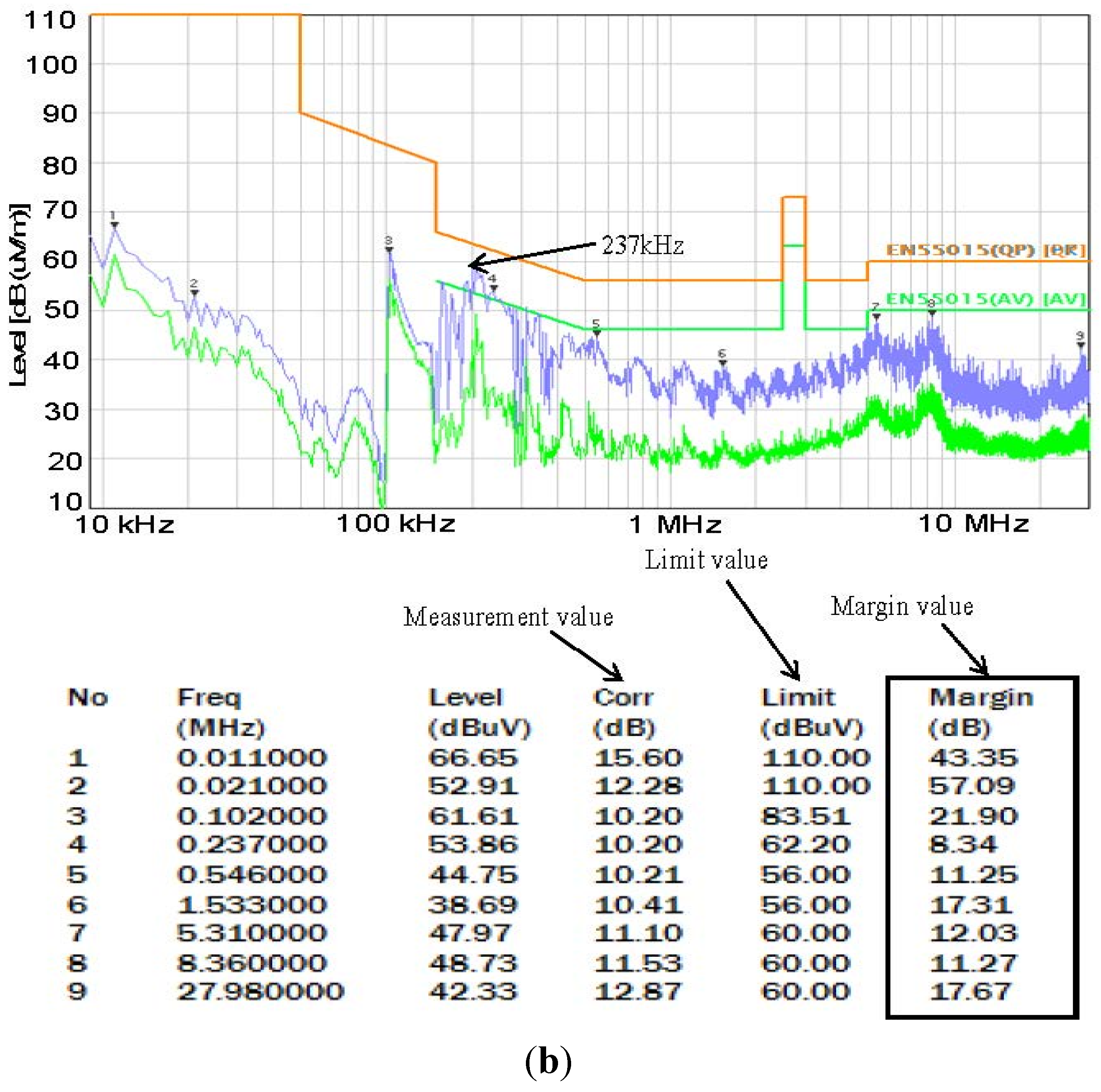
3. Experimental Results

Table 1 shows the system specification of the proposed converter.
Table 1. System specification of the proposed converter.
ComponentPartDescription
Drive ICPFCSCY99102 (Onsemi)
LLCL6599 (STmicro)
MOSFET Q 1 , Q 2 STF13NM60 (STmicro) 600 V/13 A
Transformer T 1 EPC3842 (Crova Hiteck) 51T:35T:35T (650 μH:350 μH:350 μH) Lr = 220 μH
T a EE2020 (Crova Hiteck) 100T:100T (3 mH:3 mH)
Capacitor C r Flim-Cap 10 nF/630 V (Pilkor) × 2 EA (20 nF)
C B Flim-Cap 22 nF/630 V (Pilkor)
C a 1 , C a 2 Ceramic-Cap 1 μF/100 V (Murata) × 2 EA serial (2 μF)
Diode D a 1 , D a 2 STTH8T06 (STmicro) 600 V/8 A
Table 2 shows a comparison of the presented converter and a conventional converter. As shown, the proposed converter can reduce the quantity of the IC, MOSFET, aluminum capacitor, and diode, etc. for each channel. Figure 20 is a photograph of the proposed converter.
Table 2. Comparison between the proposed converter and a conventional converter.
ComponentPartConventional ConverterProposed Converter
ICPFC, LLC2 EA2 EA
Buck4 EA0 EA
MOSFET Q 1 , Q 2 2 EA2 EA
Buck4 EA0 EA
Transformer T 1 1 EA1 EA
T a 0 EA2 EA
InductorBuck4 EA0 EA
Capacitor C r , C B 1EA (CB 0 EA)2 EA
E-Cap5 EA0 EA
DiodeLLC2 EA0 EA
Buck4 EA0 EA
Proposed0 EA4 EA
Total29 EA13 EA
Figure 20. Photograph of the proposed converter.
Energies 08 02125 g020
The experiments are performed with the proposed converter, which is designed for a 140 Watt multi-LED driver. Two 95 Vdc (300 mArms) LED loads and two 120 Vdc (300 mArms) LED loads are applied for multi LED loads.
Figure 21 shows the test waveforms of the LLC converter under full load condition. Channel 1 is the waveform of the transformer’s primary side voltage ( V L m ), Channel 2 is the waveform of the transformer’s primary side current ( I P ), and channel 3 is the waveform of the transformer’s secondary side current. In the case of channel 3, a 90 degree phase difference occurs according to the winding direction, and the current path is determined according to the voltage difference among each channel.
Figure 21. Test waveforms of LLC converter under the full load condition.
Energies 08 02125 g021
Figure 22 shows the LED voltage and current in the cases where the converter is turned on and off. The proposed converter performs stable turn on and soft turn off without an abnormal spike or malfunction.
Figure 22. LED voltage and current in the case where the converter is turned on and off. (a) Turn on; (b) Turn off.
Energies 08 02125 g022
Figure 23 shows the output voltage-current waveform at under 100% and 10% brightness condition. As shown, a constant current control is performed according to dimming control.
Figure 23. Output voltage-current waveform under 100% and 10% brightness condition; (a) Ch1~Ch4 output voltage-current waveform under 100% brightness condition; (b) Ch1~Ch4 output voltage-current waveform under 10% brightness condition.
Energies 08 02125 g023
Figure 24 shows the electrical characteristics of the proposed converter at 220 Vac condition. At the 136.92 Watt input power, efficiency is calculated to be 93% with four channel LED loads (94.5 V × 0.301 A + 118 V × 302 A + 93.7 V × 0.300 A + 117.1 V × 0.302 A = 127.55 Watt). The power factor (λ1) is 0.97. In the case of THD, the ratio of current is limited with the harmonic order. According to KC standards (K61000-3-2) [13], a third harmonic current requires less than PF × 30% and a fifth harmonic current requires less than PF × 10% of fundamental wave. As shown at Figure 24, the total harmonic distortion of input current ( I T H D 1 ) is 15.642%, the ratio between the third harmonic current and the fundamental current (I1(1)) is 13.842% (0.0875 A/0.6321 A × 100%), and the ratio between the third harmonic current and the fundamental current (I1(1)) is 6.581% (0.0416 A/0.6321 A × 100%), thus the proposed converter satisfies the KC standard (K61000-3-2).
Figure 24. Electrical characteristics of the proposed converter.
Energies 08 02125 g024
Figure 25 shows the EMI test result of the proposed converter. Figure 25a shows the Radiation Emission (RE) result. The maximum noise value is 22.3 dBμV/m at 61.909 MHz, and at this point, has a 7.7 dB margin according to the standard CISPR 15 Class B. Figure 25b shows the Conduction Emission (CE) result. The minimum margin value is 8.34 dB at 237 kHz according to CISPR 15 Class B.
Figure 25. EMI test results. (a) EMI RE Test result; (b) EMI CE Test result.
Energies 08 02125 g025aEnergies 08 02125 g025b

4. Conclusions

LEDs have high luminous efficiency and 20%~30% saving cost effect compared to a conventional light source. Therefore, research and development on an LED driver has recently been actively carried out. Generally, LED’s can be configured with a variety of operating voltages and currents. Also, LED’s have the advantage of being able to have a multi-string channel. A conventional multi LED driver system uses an individual LED driver for each channel and this induces the need for many components, reduces the system life time, and has low efficiency.
In this paper, a novel method for a multiple LED driver converter using capacitor and transformer current balancing is proposed. The proposed converter has considerably fewer components and thus saves space compared to the conventional converter. The proposed converter consists of four blocks: (1) the PFC block for high power factor implementation; (2) a half bridge block to generate a square wave voltage with 380 Vdc input; (3) and (4) both blocks consist of a resonant tank and balanced capacitor-transformer circuit. The proposed converter operates using ZVS commutation to achieve high efficiency and to improve the EMI. Through the theoretical analysis and experiments, the proposed converter is analyzed and verified. In the experimental results, the proposed converter was measured at a high power factor (over 0.9) and high efficiency (over 90%) performance. In addition, the EMI and THD characteristics were verified for the reliability of the converter.

Author Contributions

Jae-Hyun Han collected experimental data and prepared figures, Young-Cheol Lim and Jae-Hyun Han wrote and reviewed the manuscript.

Nomenclature

f o , f min
resonant frequency and minimum resonant frequency
L b 1 , L b 2
primary and secondary side inductance of the balanced transformer T a
L l k
leakage inductance of primary side T 1
L m
magnetization inductance of transformer T 1
L p
primary side inductance of transformer T 1
L r , C r
inductance and capacitance of resonant tank
Av
transfer gain of equivalent tank circuit
n
transformer turn ratio
N P , N S
number of turns in the primary and secondary coils respectively
Q
quality factor of equivalent tank circuit
R e q
an equivalent resistive value of the LED
R L
load resistance of equivalent circuit
R L 1 , R L 2
an equivalent resistive value of the L E D a 1 and L E D a 2
V C B , I C B
voltage and current of capacitor C B
v D a 1 , v D a 2
voltage of diode D a 1 , D a 2
v L E D a 1 , v L E D a 2
voltage of L E D a 1 , L E D a 2
V o , I o , P o
output voltage and current and power of equivalent circuit
V o a , I o a , R o a
load voltage and current and resistance of equivalent circuit (fundamental approximation)
V S
voltage across the secondary side of transformer T 1
v T a 1 , v T a 2
primary and secondary side voltage of transformer T a

Conflicts of Interest

The authors declare no conflict of interest.

References

  1. Tan, Y.K.; Huynh, T.P.; Wang, Z. Smart personal sensor network control for energy saving in DC grid powered LED lighting system. IEEE Trans. Smart Grid 2013, 4, 669–676. [Google Scholar] [CrossRef]
  2. Lv, X.; Loo, K.H.; Lai, Y.M.; Tse, C.K. Energy-saving driver design for full-color large-area LED display panel systems. IEEE Trans. Ind. Electron. 2014, 61, 4665–4673. [Google Scholar] [CrossRef]
  3. Hui, S.Y.R.; Chen, H.; Tao, X. An extended photoelectrothermal theory for LED systems: A tutorial from device characteristic to system design for general lighting. IEEE Trans. Power Electron. 2012, 27, 4571–4583. [Google Scholar] [CrossRef] [Green Version]
  4. Zhang, J.; Xu, L.; Wu, X.; Qian, Z. A precise passive current balancing method for multioutput LED drivers. IEEE Trans. Power Electron. 2011, 26, 2149–2159. [Google Scholar] [CrossRef]
  5. Zhao, C.; Xie, X.; Liu, S. Multioutput LED drivers with precise passive current balancing. IEEE Trans. Power Electron. 2013, 28, 1438–1448. [Google Scholar] [CrossRef]
  6. Lin, R.L.; Chang, Y.C.; Lee, C.C. Optimal design of LED array for single-loop CCM buck-boost LED driver. IEEE Trans. Ind. Appl. 2013, 49, 761–768. [Google Scholar] [CrossRef]
  7. Kim, M.G. Error amplifier design of Peak Current Controlled (PCC) buck LED driver. IEEE Trans. Power Electron. 2014, 29, 6789–6795. [Google Scholar] [CrossRef]
  8. Zhang, F.; Ni, J.; Yu, Y. High power factor AC-DC LED driver with film capacitors. IEEE Trans. Power Electron. 2013, 28, 4831–4840. [Google Scholar] [CrossRef]
  9. Lee, A.T.L.; Sin, J.K.O.; Chan, P.C.H. Scalability of quasi-hysteretic fsm-based digitally controlled single-inductor dual-string buck LED driver to multiple strings. IEEE Trans. Power Electron. 2014, 29, 501–513. [Google Scholar] [CrossRef]
  10. Zhang, R.; Chung, H.S.H. Transformer-isolated resonant driver for parallel strings with robust balancing and stabilization of individual LED current. IEEE Trans. Power Electron. 2014, 29, 3694–3708. [Google Scholar] [CrossRef]
  11. Hasan, J.; Ang, S.S. A high-efficiency digitally controlled RGB driver for LED pixels. IEEE Trans. Ind. Appl. 2011, 47, 2422–2429. [Google Scholar] [CrossRef]
  12. Lo, Y.K.; Wu, K.H.; Pai, K.J.; Chiu, H.J. Design and implementation of RGB LED drivers for LCD backlight modules. IEEE Trans. Ind. Electron. 2009, 56, 4862–4871. [Google Scholar] [CrossRef]
  13. Ng, S.K.; Loo, K.H.; Lai, Y.M.; Tse, C.K. Color control system for RGB LED with application to light sources suffering from prolonged aging. IEEE Trans. Ind. Electron. 2014, 61, 1788–1798. [Google Scholar] [CrossRef]
  14. Feng, W.; Lee, F.C.; Mattavelli, P. Optimal trajectory control of LLC resonant converters for LED PWM dimming. IEEE Trans. Power Electron. 2014, 29, 979–987. [Google Scholar] [CrossRef]
  15. Hong, S.W.; Kim, H.J.; Park, J.S.; Gun, Y. Secondary-side LLC resonant controller IC with dynamic PWM dimming and dual-slope clock generator for LED backlight units. IEEE Trans. Power Electron. 2011, 26, 3410–3422. [Google Scholar] [CrossRef]
  16. Cheng, C.A.; Cheng, H.L.; Chung, T.Y. A novel single-stage high-power-factor LED street-lighting driver with coupled inductors. IEEE Trans. Ind. Appl. 2014, 50, 3037–3045. [Google Scholar] [CrossRef]
  17. Wu, X.; Zhang, J.; Qian, Z. A simple two-channel LED driver with automatic precise current sharing. IEEE Trans. Ind. Electron. 2011, 58, 4783–4788. [Google Scholar] [CrossRef]
  18. Kim, J.K.; Lee, J.B.; Moon, G.W. Isolated switch-mode current regulator with integrated two boost LED drivers. IEEE Trans. Ind. Electron. 2014, 61, 4649–4653. [Google Scholar] [CrossRef]

