A Generalized Approach for the Steady-State Analysis of Dual-Bridge Resonant Converters


Abstract
: In this paper, a dual-bridge DC/DC resonant converter with a generalized series and parallel resonant tank is analyzed. A general approach based on Fundamental Harmonic Approximation is used to find the universal steady-state solutions. The analysis results for particular resonant tank configurations are exemplified with several typical resonant tank configurations respectively. The corresponded soft-switching conditions are discussed too. To illustrate the usefulness of the generalized approach, a dual-bridge (LC)(L)-type resonant converter working in below resonance mode is designed based on the analysis results. Finally, simulation and experimental plots of the design example are included to evaluate the validity and the accuracy of the proposed analysis approach.1. Introduction
Since its introduction several decades ago, resonant DC/DC converters have drawn much attention from both industrial engineers [1] and academic researchers [2–9] and have been used in real applications such as consumer electronics products and distribution generation. Different arrangements of resonant tank have been examined to create nearly sinusoidal waveforms and soft switching operation, which in turn enable higher switching frequency and small converter size. Two main control methods, varying frequency and fixed frequency phase-shift control, could be used to control power flow [1–7]. To realize Zero-Voltage Switching (ZVS) in varying frequency control, above resonance or lagging mode operation is preferred with the switching frequency higher than the resonance frequency. Naturally a wide spectrum of voltage and current harmonics would be resulted, which may bring audible noise and high EMI. Consequently the requirement for the design of all frequency-sensitive components including filters, reactive components and magnetic devices would be strict and the total cost would rise. Fixed frequency control of resonant converters, i.e., the so-called phase-shift control, which is limited to full-bridge type resonant converter, suffers from asymmetric switching behavior in two switch legs. Half of the main switches may lose ZVS at light load.
Another popular high-frequency (HF) isolated DC/DC converter reported in the literature is a dual-active-bridge (DAB) converter [10,11], which is featured with simple phase-shift control, high power density and bidirectional power flow. The bidirectional power transfer depends on the AC-link inductor, which includes the leakage inductor of the HF transformer through fixed frequency phase-shift control between two active bridges. Different switching strategies to limit output circulation current and improve efficiency for DAB have been discussed extensively in the literature [12–18].
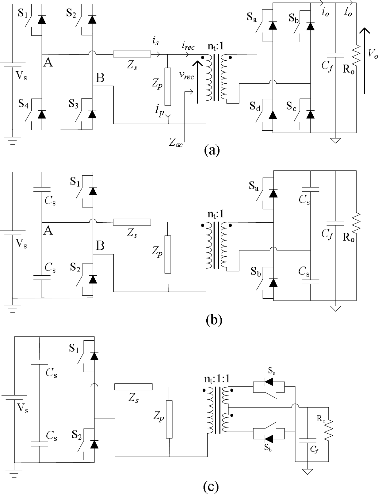
A dual-bridge resonant converter (DBRC) can be regarded as a DAB equipped with a resonant tank. As seen in Figure 1, a DBRC includes the two active bridges across the HF transformer, which can be implemented as either full bridge or half-bridge with different transformer structure types. Although the inserted resonant tank has so many different configurations [3–5], the combination of a series Zs and a parallel Zp could represent most frequently discussed configurations in the literature. Both Zs and Zp are interconnections of a number of inductors and capacitors. Through proper design and arrangement, the leakage and magnetic inductance of the HF transformer might be integrated into the resonant tank possibly. According to the hybrid structure, the DBRC inherits most features of both DAB and conventional resonant converter. Similar to the DAB, the converter is able to provide bidirectional power flow by simply varying the phase-shift between the two square-wave voltages generated by the two active bridges. Due to the existence of resonant tank, most of the voltages and currents in the DBRC have nearly sinusoidal forms. With many available options of the configurations of resonant tank, DBRC would have more flexibilities to realize soft-switching operation.
Conventionally, two different approaches can be applied for the steady-state analysis of resonant converters. (1) At the cost of complicated calculation, the differential equation or state-space approach can give accurate results. When the number of reactive components is high, it would be quite difficult to solve the resulted high-order differential equations and the close-form analytic solutions may be impossible to obtain. (2) Compared with the first approach, frequency domain approach using Fourier series analysis would be easier to implement. Based on the principle of superposition, a compromise between the accuracy and the complexity can be manipulated by means of a proper selection of the number of harmonics involved in the calculation. The so-called complex AC-circuit analysis or fundamental harmonics analysis (FHA) can be regarded as a special case with only fundamental component considered. In [19,20], a modified FHA is proposed for a dual-bridge series resonant converter (DBSRC) with either resistive load or voltage source load. In this paper, the proposed modified FHA approach would be applied for the steady-state analysis of a dual-bridge resonant converter with a generalized series-parallel resonant tank as show in Figure 1. The features that the paper tends to show are listed as follows. The selected approach can be used for the steady-state analysis of a DBRC with a generalized series-parallel tank. The obtained results could be used for the evaluation of soft-switching conditions and a fast initial design. Furthermore, the general results can be applied for most of the commonly used resonant tanks with minor modification.
This rest of the paper is organized as follows. The steady state in a DBRC with a series-parallel resonant tank is analyzed by a modified FHA approach at first. Switch stresses and soft-switching conditions are derived. Then the general analysis results are discussed for several particular configurations of resonant tanks respectively. A design example using an (LC)(L)-type resonant tank is given based on the analysis results. Verification is performed by means of both PSIM simulation and actual experimental tests.
2. Steady-State Analysis in Frequency Domain
In this section, the modified FHA approach would be used for the steady-state analysis of DBRC with a series-parallel tank. Although the FHA is equivalent to the fundamental version of Fourier series approach, it presents the results using a unique view angle from the load side to include the effects of secondary active switching. FHA is also easy to calculate and suitable for quick estimations of steady-state parameters and a fast initial converter design.
2.1. Assumption and Notation
To simplify the analysis process, all switches, diodes, inductors, capacitors and the HF transformer in the converter are assumed to be ideal and lossless. Snubber circuit effects are neglected too. For convenience, all quantities located on the secondary side of the HF transformer have been transferred to the primary side, which are marked by the apostrophe. Additionally, all quantities presented are normalized with the base values below:
2.2. Modified Fundamental Harmonics Approximation
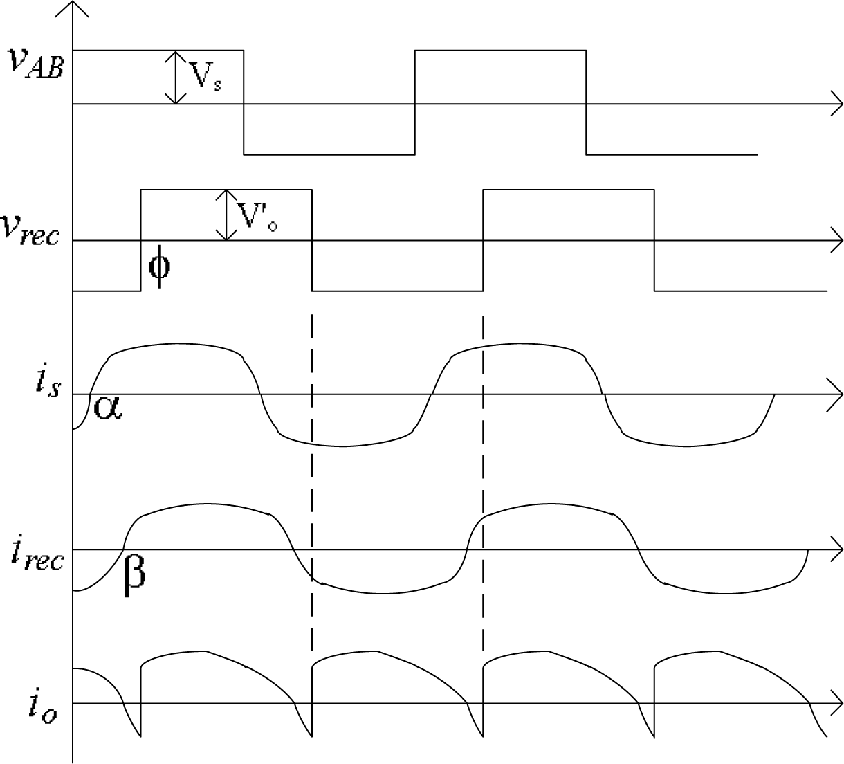
As a simplified version in frequency domain approach, only the fundamental components of all voltages and currents are considered in FHA. The rationale originates from the nature resonance phenomena, i.e., most voltages and current are nearly sinusoidal. Thus, to neglect the effects of high-order harmonics would not reduce the accuracy too much. The typical steady-state waveforms of several important voltages and currents are shown in Figure 2.
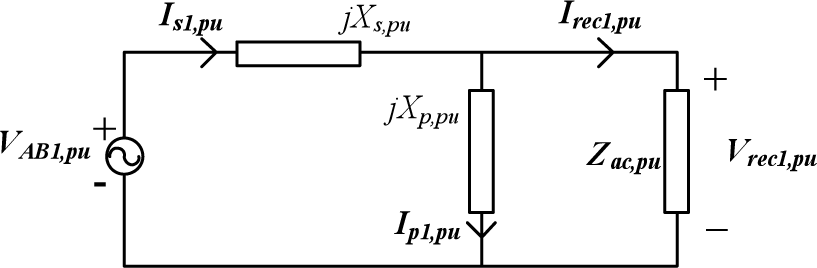
It is seen that both vAB and vrec are square-wave with a controlled phase-shift ϕ between them, whose amplitudes are Vs and respectively. The output current io is obtained from the transformer secondary current i2 by active rectification, whose average value is the load current Io. The key step in FHA is to represent the load side including the HF transformer by an equivalent impedance Zac. In the conventional FHA used for regular resonant converters with capacitive output filter, this impedance is purely resistive due to the HF diode rectifier. However, it could not always be resistive in a DBRC since the secondary bridge is actively controlled now. According to the waveforms shown in Figure 2, the normalized fundamental peak values of vrec and irec can be found as:
Thus, the fundamental equivalent circuit of the DBRC in phasor domain can be drawn like Figure 3. In phasor domain, the fundamental phasor of the input square-wave voltage source vAB shown in Figure 2 is given as:
According to Figure 3, the resulted resonant current phasor could be calculated as:
After being converted into time domain, the corresponding fundamental resonant current is1,pu(t) is expressed as:
Following the same principle, the fundamental primary current irec1,pu(t) is expressed as:
The fundamental parallel branch current ip1,pu(t) is given as:
The complex voltage gain in Figure 3 is defined as:
With the help of Equation (15), the expression of fundamental converter gain is shown to be:
With the assumption of lossless power transfer, the complex fundamental output power is given as:
The fundamental output active power P1,pu and reactive power Q1,pu can be evaluated as:
The polarity of active power depends on both the reactance of series resonant tank Xs,pu and the phase-shift ϕ. With the assumption of an inductive series resonant tank (i.e., Xs,pu > 0), ϕ can be controlled in either [0, π/2] or [π/2, π] to transfer a certain amount of positive active power. However, when delivering the same amount of active power, the absolute value of reactive power generated in the case of [π/2, π] is definitely higher than that in the case of [0, π/2], which indicates high circulating current. If Xs,pu < 0, a negative phase-shift ϕ ∈ [−π/2, 0] can also result in a positive active power.
2.3. Soft-Switching Conditions
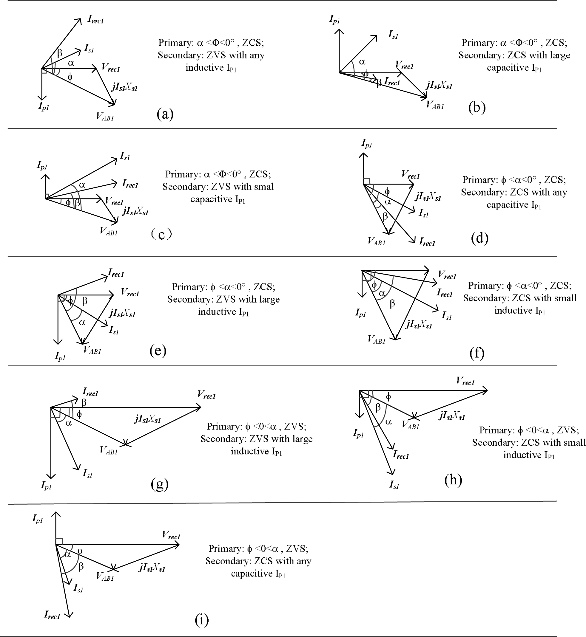
The soft-switching situation in the DBRC can be identified by the phase angles between some particular phasors. The necessary ZVS condition in the primary bridge is that is1 lags vAB1. The necessary ZVS condition in the secondary bridge is that irec1 leads vrec1.
With the assumption of an inductive Xs,pu, the possible soft-switching situations with the corresponding phasor diagrams are listed in Figure 4. The angle ϕ is assumed to be larger than zero for positive power flow. On the primary side, if α > 0 for Figure 4a–f, then the primary side switches can work in ZVS, otherwise the primary switches would work in ZCS for Figure 4g–i. On the secondary side, as long as α < ϕ, the switches on the secondary bridge can work in ZVS for either any inductive parallel ip (Figure 4a,g) or a small capacitive parallel ip (Figure 4b,h). A large capacitive ip would result in ZCS on the secondary side (Figure 4c,i). If α > ϕ, the switches on the secondary bridge will work in ZCS for either any capacitive ip (Figure 4f) or a small inductive parallel ip (Figure 4e). Only a large inductive ip may enable ZVS on the secondary side (Figure 4d).
In the case of a capacitive series resonant tank, the resulted soft-switching conditions would show a duality relationship compared with the above case. The detail can be understood easily with the help of Figure 5. The angle ϕ is assumed to be negative for positive active power flow. On the primary side, if α > 0 for Figure 5g–i, then the primary side switches can work in ZVS, otherwise the primary switches would work in ZCS for Figure 5a–f. On the secondary side, if α < ϕ, the switches on the secondary bridge can work in ZVS for either any inductive parallel ip (Figure 5a) or a small capacitive parallel ip (Figure 5c). A large capacitive ip would result in ZCS on the secondary side (Figure 5b). If 0 > α > ϕ, the switches on the secondary bridge will work in ZCS for either any capacitive ip (Figure 5d) or a small inductive parallel ip (Figure 5f). Only a large inductive ip may enable ZVS on the secondary side (Figure 5e).
Also, with the help of the analysis results, the necessary conditions of ZVS in the primary and secondary bridges could be concluded as:
After simplifications, the two ZVS conditions can be rewritten as:
Normally the series resonant tank is composed of an inductor or a series connection of LC working in above resonance condition so that Xs,pu is positive. Thus, to realize ZVS in both bridges, the ideal necessary solution is concluded as:
To satisfy Equation (24), it is desirable that both 1/M and M(1 + Xs,pu/Xp,pu) are larger than 1 since the maximum of cos ϕ is 1 at no load. It is noted that if M ≤ 1 the ZVS operation of the primary bridge can be maintained from full load to zero load (as shown in Figure 4a–f). Once M is fixed, the ratio Xs,pu/Xp,pu shall be chosen properly to make 1 ≤ M(1 + Xs,pu/Xp,pu) so that the ZVS in the secondary bridge can be maintained for a wide range of load. It should be noted that the associated high circulation current from a high Xs,pu/Xp,pu would be a penalty.
Although hardly found in literature, the series resonant tank could be capacitive, for example, when a series connection of LC is operated with a switching frequency below the resonance frequency. Thus, the ZVS conditions in two bridges are:
Apparently Equation (25) gives a solution opposite to Equation (24). It seems that the two schemes will have mirrored operation with same power transfer capability theoretically. For actual application, those two schemes may differ from each other in terms of the size of reactive components and switch stress.
It can be concluded from the above analysis that the active power transfer and the soft-switching condition in the primary bridge are affected by the series resonant tank. Without impact on the power transfer, the parallel resonant tank contributes to the soft-switching operation of the secondary bridge only.
3. Analysis Results for Particular Tanks
In this section, the analysis results for several particular configurations of resonant tank that were studied frequently in the literature are discussed individually. The subscript “s” and “p” of L or C denotes the component in the series tank Zs or the parallel tank Zp respectively. Two ratios are defined as:
The base frequency is chosen the same as the series resonance frequency ωr:
The normalized switching frequency F and the quality factor Q are defined as:
Thus, the normalized reactance of inductors and capacitors in Zs and Zp can be expressed as: XLs,pu = QF; XCs,pu = −Q/F; XLp,pu = QFKL; XCp,pu = −Q/(KCF).
3.1. A Two-Element Tank: (LC) Type
The standard SRC (series resonant converter) has a series LC tank and has no parallel tank. The transformer leakage inductance can be included into the series inductance and the transformer magnetizing inductance should be made as large as possible. Since there is no parallel tank (Xp,pu = ∞), the resonant current is is equal to the transformer current irec. The converter gain and peak resonant current are:
According to Equation (18), if F > 1, the phase-shift ϕ should be positive to enable a power flow from the primary to the secondary. If F < 1, the phase-shift ϕ should be negative to enable a power flow from the primary to the secondary. The necessary ZVS condition is given as:
The ZVS range for F > 1 is found the same as that of a DAB [10,11]. Only M = 1 can meet the ZVS requirements of both bridges at the same time. When F < 1, no value of M can let both sides work in ZVS at the same time.
3.2. A Three-Element Tank: (LC)(L) Type
The (LC)(L) type series resonant converter has a series LC tank and a parallel inductor tank. The transformer leakage inductance and magnetizing inductance can be utilized as part of the resonant tank. The converter gain and resonant peak current have the same expression as those in the case of (LC) tank. The other peak currents are shown as:
The necessary ZVS conditions in both of bridges are given as:
For F > 1, it is possible to achieve ZVS operation in both bridges for any phase-shift : the maximum of M is chosen not more than one for full ZVS operation on the primary side, and then the inductor ratio KL can be manipulated to keep ZVS when M is minimum to fulfill ZVS operation on the secondary side.
For F < 1, it is possible to achieve ZVS operation in both bridges for a range of phase-shifts ϕ ∈ [ϕmax, 0]: the minimum of M is chosen larger than one when ϕ = ϕmax, so that ZVS operation on the primary side is secured, and then the inductor ratio KL can be manipulated to keep ZVS on the secondary side when M is maximum. It can be concluded from Equations (36) and (37) that KL is preferred to be smaller for both cases to achieve a wide range of ZVS operations. The side-effect brought by a small KL is a high current flowing in the parallel tank.
3.3. A Three-Element Tank: (LC)(C) Type
The series-parallel (LC)(C) type resonant converter has a series LC tank and a parallel capacitor tank. The converter gain and resonant peak current have the same expression as those in the case of (LC) tank. The parallel capacitor peak current is given as:
The transformer current irec has the same expression as Equation (34) with a different A3 as:
The necessary ZVS conditions in both of the bridges are given as:
For F > 1, it is possible to achieve ZVS operation in both bridges for a range of phase-shifts at heavy load. At light load when ϕ is approaching zero, one of the two bridges will enter into ZCS definitely. For F < 1, it is impossible to achieve ZVS operation simultaneously in both bridges for any phase-shift ϕ even if M = 1.
In conclusion, the parallel resonant tank is expected to provide an inductive current so that the ZVS range of the secondary bridge can be extended. Also, the satisfaction of Equations (24) and (25) cannot guarantee ZVS in actual operation due to the existence of snubber circuit and parasitic components, thus some margin should be given in actual design.
4. Validation Using an (LC)(L) DBRC with F < 1
To examine the validity of the steady-state analysis above, the design, simulation and experimental test of a full-bridge (LC)(L) dual-bridge resonant converter working in below resonance mode are presented in this section.
4.1. Design
The converter to be designed is to be used as a battery charger between a DC bus and a battery stack. The rated output power is assumed at Po = 200 W. The input voltage Vs = 100 V is assumed constant and the output voltage has a deviation of 10% (Vo = 43.2–48 V) i.e., Mmin = 0.9 Mmax. The switching frequency is 100 kHz.
The designed converter is supposed to work in below resonance mode. According to discussions in [19,21] for F > 1, the resonant current is quite sensitive to the normalized switching frequency F. A value of F near 1 is helpful to reduce the peak resonant current, which is also true for F < 1. The value of quality factor Q has impact on both resonant current and the size of resonant tank. A small Q can result in small resonant tank. Finally, F = 0.9, Q = 1 is chosen in this work.
The design objective is to achieve wide ZVS operation range as the load varies. As indicated by Equation (37), the ZVS operation on the primary side relies on the converter gain M solely and both M and KL need to be manipulated for ZVS operation in the secondary bridge. According to Equation (16), the maximum phase-shift ϕmax happens at Mmin. If Mmin is purposely selected to satisfy cos ϕmax = 1/Mmin, then cos ϕ > 1/M is always true for the whole range of output voltage and load and ZVS on the primary is secured. After calculation, the converter gain are found to be Mmin = 1.064 and Mmax = 1.183. The phase-shifts under those two conditions are ϕmax = −19.57° and ϕrate = −17.94° (the phase-shift for rated power at Mmax) respectively. The HF transformer turns ratio is calculated as: nt = Mmax ·· Vin/Vomax = 2.46. Thus the reflected full load resistance is . Then, the resonant tank can be obtained as: Ls = 100.22 μH, Cs = 20.47 nF. The inductor ratio KL can be determined at Mmax with ϕrate = −17.94°. With the help of Equation (37)KL is set to 1.2 and Lp is 120 μH. The specifications of the (LC)(L)-type DBRC working in below resonance mode are concluded in Table 1. With this design scheme, the converter is supposed to work as described in (vii) of Figure 5.
4.2. Simulation Results
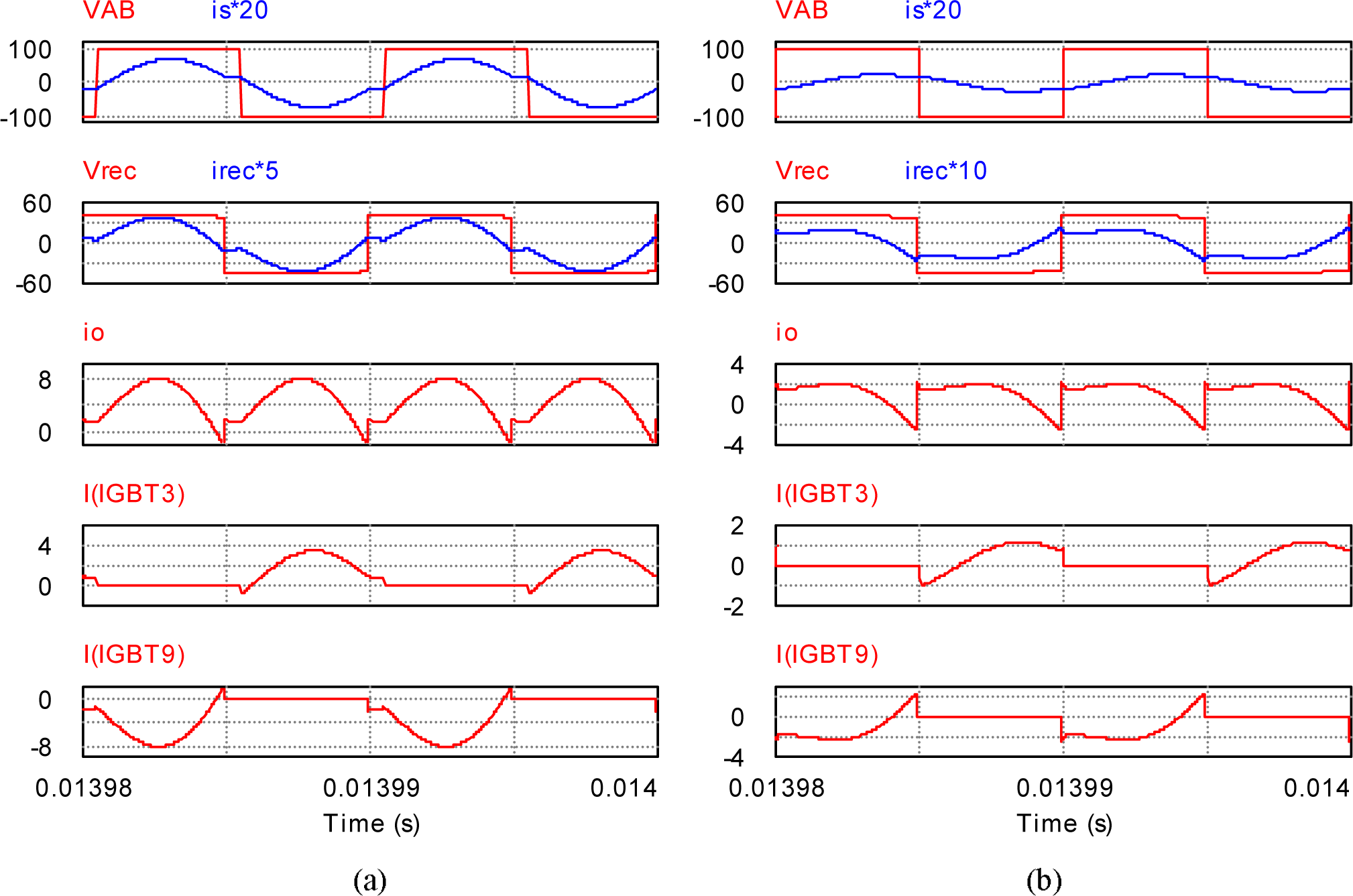
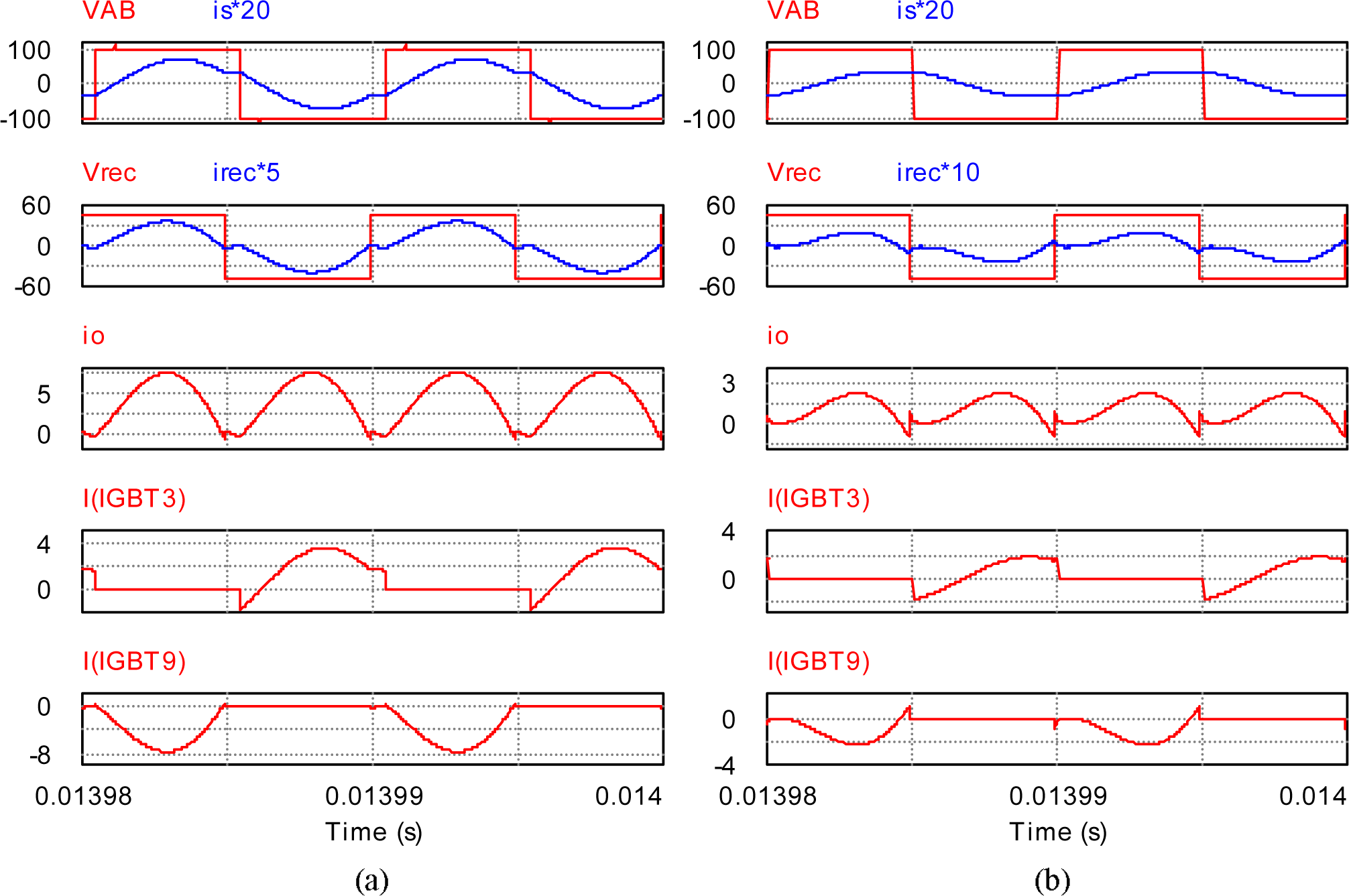
Firstly the (LC)(L)-type dual-bridge converter is simulated in PSIM 9.0. In order to mimic actual operation, more non-ideal parameters are included in simulation setup: the dead-band is set at 3° or 83.3 ns, on-state voltage-drop of switch is set at 1 V, turn-on voltage of anti-parallel diode is set at 0.7 V. The operation conditions with output voltage Vo = 43.2 V and Vo = 48 V are shown in Figures 6 and 7 respectively. For each of two cases, both full load and 25% load operational conditions are presented.
The two square waveform voltages vAB, vrec (on the secondary side) are shown with their bridge currents is, irec (on the secondary side) together, respectively. Soft-switching condition can be checked by means of the switch currents in each of the two bridges (iIGBT3 is one of switch currents on the primary, iIGBT9 is one of switch currents on the secondary). It can be found that ZVS operation could be held for the full range of load. Although the waveforms of output current io show some circulation current for all test conditions, the portion of circulation current is quite small even at light load.
4.3. Experimental Results
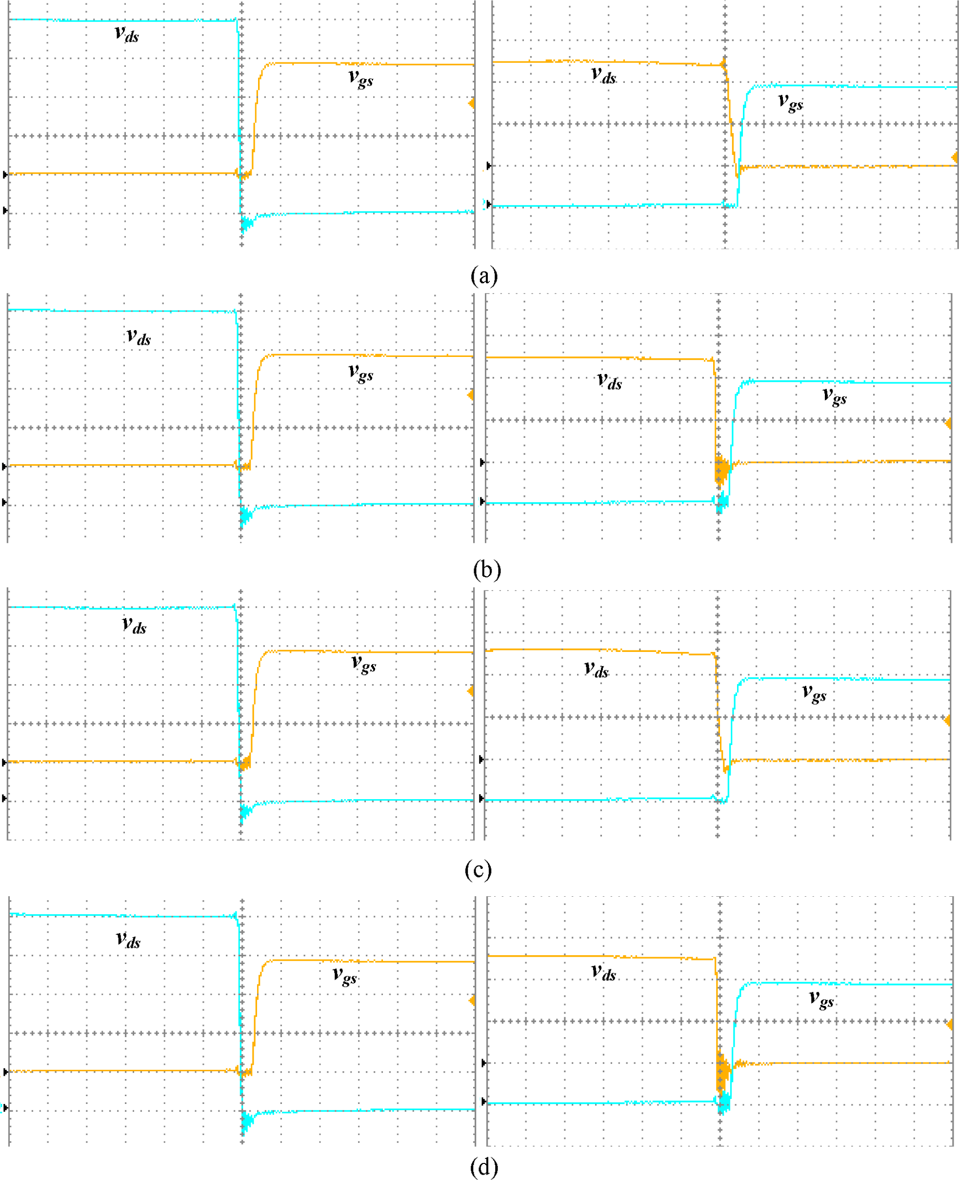
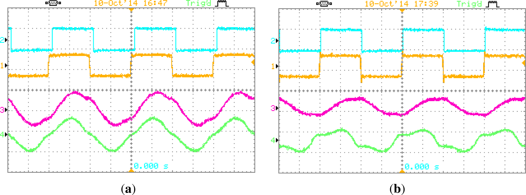
To verify the validity of the steady-state analysis further, a lab prototype of the (LC)(L)-type dual-bridge resonant converter was built and tested. The core of the HF transformer is one pair of EPCOS ETD39 core (material N97). The winding are made of multi-thread Litz wire with a transformer turns ratio of 22:9. The magnetic inductance is measured at 1.8 mH. The primary reflected total equivalent leakage inductance is measured at 4.85 μH. Thus an external series inductor of 96μH is added. Both the series inductor and the parallel inductor are built with the toroidal core (material Ni–Fe permalloy). The two shifted gating signals are generated from an eZdspF2812 DSP development board. The eight main switches used in the two bridges are IRFR4620.
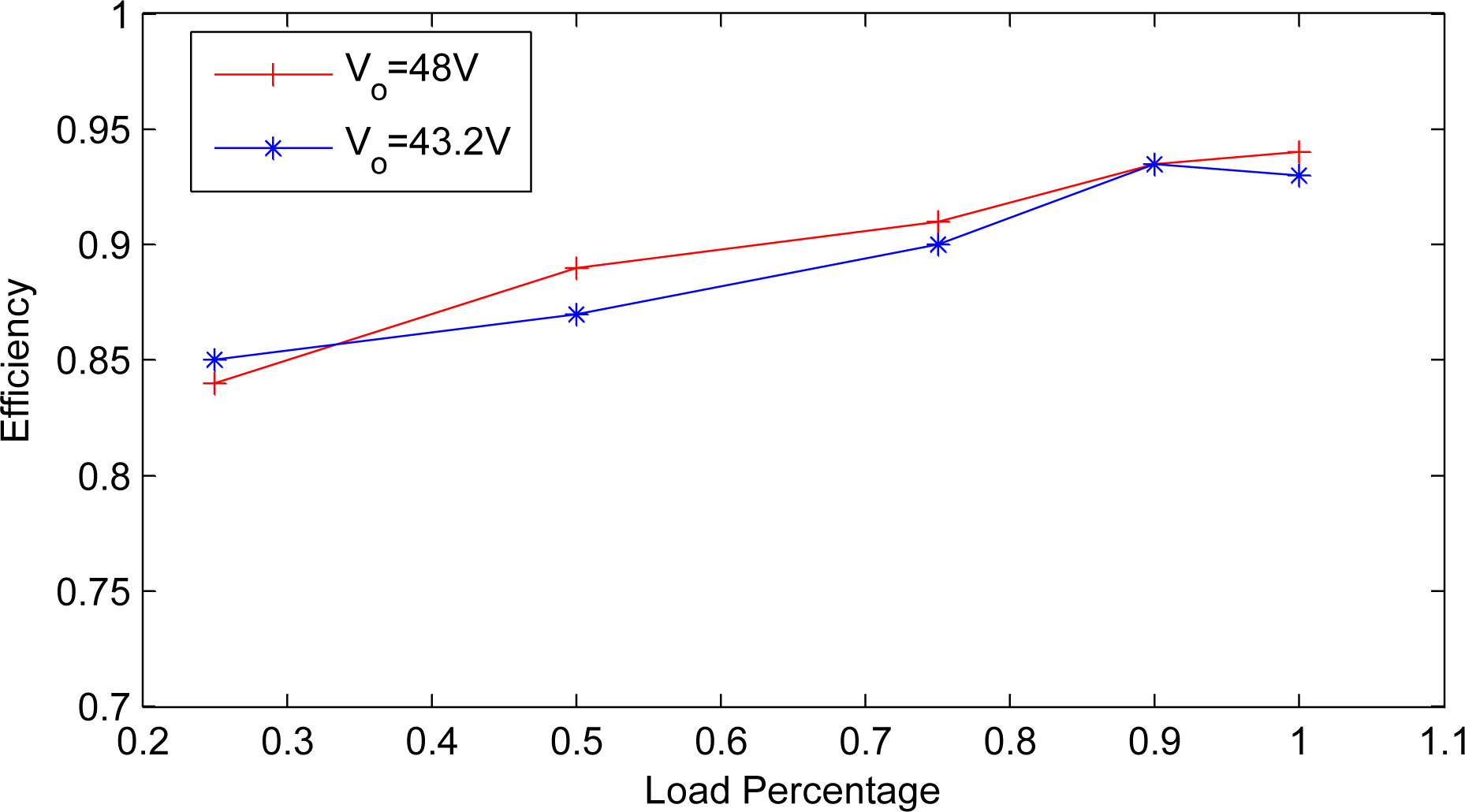
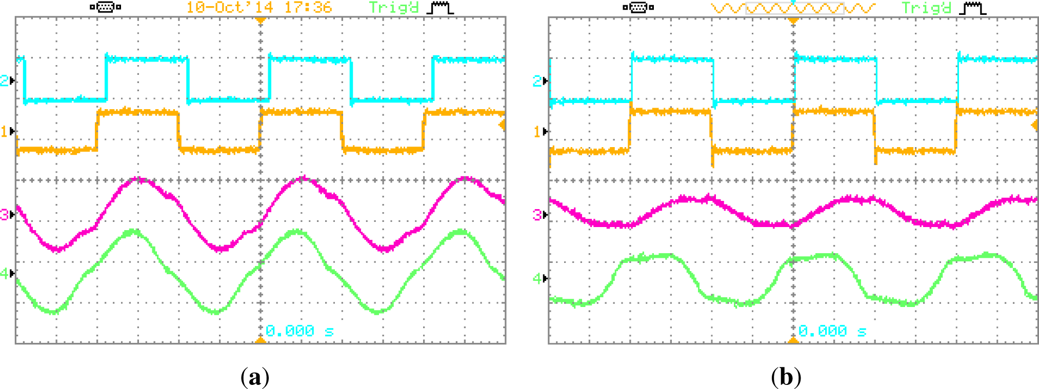
The experimental plots of Vo = 48 are presented in Figure 8, which consists of test situations for full load and 25% load respectively. The experimental plots of Vo = 43.2 V under the same conditions are given in Figure 9. At heavy load, the parallel current ip does not affect irec too much. However, the effect of ip on irec becomes apparent at light load. The ZVS operation can be confirmed from Figure 10, in which the gating signals and the switch voltages are shown together. The converter efficiency at full load with Vo = 48 V and Vo = 43.2 V are 94% and 93% respectively and the efficiency curve at different load level are presented in Figure 11.
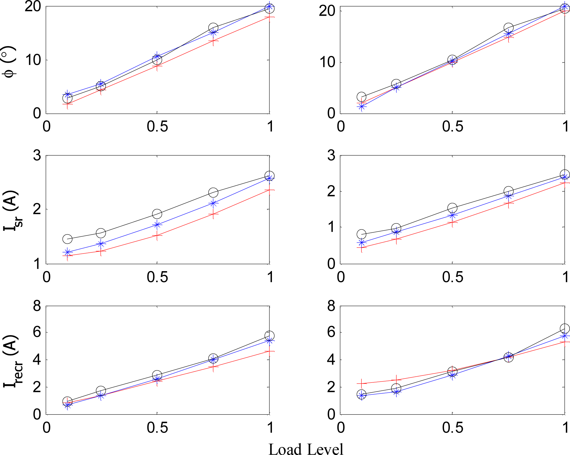
The comparison of some parameters (phase-shift ϕ, series resonant RMS current Isr and the transformer RMS current on the secondary Irecr) between the theoretical calculation (denoted by “+”), simulation values (denoted by “*”) and experimental results (denoted by “o”) are included in Figure 12. Reasonable matches can be observed for most of values. According to the design, the variation range of ϕ is relatively narrow for the whole operation range. Because sin ϕ ≈ ϕ, if ϕ is small, it can be seen that the variation of ϕ with regards to load is almost linear. The dead-band of gating signals for each complementary switch pair is neglected in theoretical calculation, but it does exist in simulation and actual implementation. Besides, the dead-band cannot be set high in simulation since the switch model in PSIM has no turn-on and turn-off delay. In addition, the switching transient in actual circuit due to HF parasitic parameters is neglected in both calculation and simulation. The parallel inductor current actually shows a triangular form instead of the assumed sinusoidal form, which is the main reason of the mismatch of currents.
5. Conclusions
With the introduction of an equivalent impedance, a modified fundamental harmonics approach is applied to a general dual-bridge resonant DC/DC converter. Although only fundamental components of all voltages and currents are considered in the analysis, the operation condition can still be predicted approximately with acceptable accuracy due to the resonance phenomenon. The ZVS conditions of different resonant tanks are derived. A design example based on a dual-bridge (LC)(L) resonant converter working under below resonance mode is presented. Simulation and experimental results are included for the purpose of validation. It is shown that the modified fundamental harmonics analysis approach for dual-bridge DC/DC resonant converter can provide satisfactory results for fast design with uncomplicated calculation.
Acknowledgments
The authors would like to thank the financial support from the Science and Technology Development Fund of Macau (FDCT) under Grant Agreement No. 067/2011/A.
Author Contributions
Gao-Yuan Hu is responsible for theoretical derivation and proving, circuit implementation and paper writing. The main contribution of Xiaodong Li is planning, coordination and consultation of the whole project. The simulation results are contributed by Bo-Yue Luan.
Conflicts of Interest
The authors declare no conflict of interest.
References
- Choi, H. Design consideration of half-bridge LLC resonant converter. J. Power Electron 2007, 7, 13–20. [Google Scholar]
- Steigerwald, R.L. A comparison of half-bridge resonant converter topologies. IEEE Trans. Power Electron 1988, PE-3(2), 174–182. [Google Scholar]
- Bhat, A. A unified approach for steady-state analysis of resonant converters. IEEE Trans. Power Electron 1991, 38, 251–259. [Google Scholar]
- Bhat, A. A generalized steady-state analysis of resonant converters using two-port model and Fourier-series approach. IEEE Trans. Power Electron 1998, 13, 142–151. [Google Scholar]
- Batarseh, I. Resonant converter topologies with three and four energy storage elements. IEEE Trans. Power Electron 1994, 9, 64–73. [Google Scholar]
- Chen, W.; Rong, P.; Lu, Z.Y. Snubberless bidirectional DC-DC converter with new CLLC resonant tank featuring minimized switching loss. IEEE Trans. Ind. Electon. 2010, 57, 3075–3086. [Google Scholar]
- Mao, M.; Tchobanov, D.; Li, D.; Maerz, M. Design optimisation of a 1 MHz half-bridge CLL resonant converter. IET Power Electron 2008, 1, 100–108. [Google Scholar]
- Selvaperumal, S.; Rajan, C. Investigation of closed-loop performance for an LCL resonant converter in a real-time operating system environment. IET Power Electron 2012, 5, 511–523. [Google Scholar]
- Jang, J.; Joung, M.; Choi, B.; Hong, S.; Li, S. Dynamic analysis and control design of optocoupler-isolated LLC series resonant converters with wide input and load variations. IET Power Electron 2012, 5, 755–764. [Google Scholar]
- De Doncker, R.W.; Divan, D.M.; Kheraluwala, M.H. A three-Phase soft-Switched high power density DC/DC converter for high power applications. IEEE Trans. Ind. Appl. 1991, 27, 63–73. [Google Scholar]
- Kheraluwala, M.H.; Gascoigne, R.; Divan, D.M.; Baumann, E. Performance characterization of a high power dual active bridge DC-to-DC converter. IEEE Trans. Ind. Appl. 1992, 28, 1294–1301. [Google Scholar]
- Jain, A.K.; Ayyanar, R. PWM control of dual active bridge: Comprehensive analysis and experimental verification. IEEE Trans. Power Electron 2011, 26, 1215–1227. [Google Scholar]
- Zhou, H.; Khambadkone, A.M. Hybrid modulation for dual-active-bridge bidirectional converter with extended power range for ultracapacitor application. IEEE Trans. Ind. Appl. 2009, 45, 1434–1442. [Google Scholar]
- Bai, H.; Mi, C. Eliminate reactive power and increase system efficiency of isolated bidirectional dual-active-bridge DC-DC converters using novel dual-phase-shift control. IEEE Trans. Power Electron 2008, 23, 2905–2914. [Google Scholar]
- Oggier, G.; Garcia, G.; Oliva, A.R. Switching control strategy to minimize dual active bridge converter losses. IEEE Trans. Power Electron 2009, 24, 1826–1838. [Google Scholar]
- Oggier, G.; Garcia, G.; Oliva, A.R. Modulation strategy to operate the dual active bridge DC-DC converter under soft switching in the whole operating range. IEEE Trans. Power Electron 2011, 26, 1228–1236. [Google Scholar]
- Shi, X.; Jiang, J.; Guo, X. An efficiency-optimized isolated bidirectional DC-DC converter with extended power range for energy storage systems in microgrids. Energies 2012, 6, 27–44. [Google Scholar]
- Jiang, J.; Bao, Y.; Wang, L.Y. Topology of a bidirectional converter for energy interaction between electric vehicles and the grid. Energies 2014, 7, 4858–4894. [Google Scholar]
- Li, X.; Bhat, A. Analysis and Design of High-Frequency Isolated Dual-Bridge Series Resonant DC/DC Converter. IEEE Trans. Power Electron 2010, 21, 850–862. [Google Scholar]
- Li, X.; Bhat, A. Ac equivalent circuit analysis for high-frequency isolated dual bridge series resonant dc/dc converter, In Proceedings of the IEEE 39th Power Electronics Specialist Conference (PESC), Rhodes, Greece, 15–19 June 2008; pp. 238–244.
- Li, X. A LLC-type dual-bridge resonant converter: analysis, design, simulation and experimental results. IEEE Trans. Power Electron 2014, 29, 4313–4321. [Google Scholar]


| Input DC Voltage | 100 V | Output DC Voltage | 43.2–48 V |
|---|---|---|---|
| Output power | 0–200 W | Switching frequency | 100 kHz |
| Series inductance Ls | 100.22 μH | Series capacitance Cs | 20.47 nF |
| Parallel inductance Lp | 120 μH | Turns ratio of the transformer | 2.46 |
© 2014 by the authors; licensee MDPI, Basel, Switzerland This article is an open access article distributed under the terms and conditions of the Creative Commons Attribution license (http://creativecommons.org/licenses/by/4.0/).
Share and Cite
Hu, G.-Y.; Li, X.; Luan, B.-Y. A Generalized Approach for the Steady-State Analysis of Dual-Bridge Resonant Converters. Energies 2014, 7, 7915-7935. https://doi.org/10.3390/en7127915
Hu G-Y, Li X, Luan B-Y. A Generalized Approach for the Steady-State Analysis of Dual-Bridge Resonant Converters. Energies. 2014; 7(12):7915-7935. https://doi.org/10.3390/en7127915
Chicago/Turabian StyleHu, Gao-Yuan, Xiaodong Li, and Bo-Yue Luan. 2014. "A Generalized Approach for the Steady-State Analysis of Dual-Bridge Resonant Converters" Energies 7, no. 12: 7915-7935. https://doi.org/10.3390/en7127915
APA StyleHu, G.-Y., Li, X., & Luan, B.-Y. (2014). A Generalized Approach for the Steady-State Analysis of Dual-Bridge Resonant Converters. Energies, 7(12), 7915-7935. https://doi.org/10.3390/en7127915