Article

Series-Parallel Inductor and Switched Capacitor Based Novel Tri Switch DC–DC Converter

1
Department of Electrical Engineering, Indian Institute of Technology, Patna 801106, India
2
Department of Electrical Engineering, University of Texas at Arlington, Arlington, TX 76019, USA
3
School of Robotics and Advanced Manufacture, Harbin Institute of Technology, Harbin 150001, China
*
Authors to whom correspondence should be addressed.
Energies 2026, 19(12), 2773; https://doi.org/10.3390/en19122773
Submission received: 8 April 2026 / Revised: 22 May 2026 / Accepted: 1 June 2026 / Published: 9 June 2026

Abstract

Decoupled maximum power point tracking control and output voltage control can be accomplished simultaneously using dual-duty cycle control. However, developed triple switch triple mode (TSTM) exhibits absence of the common ground between the solar panel and output load therefore causing the leakage current to flow which creates safety concern especially for household electrification. In addition to having a negative effect on the solar panel, leakage current increases power losses. Thus, this work proposes a unique TSTM dc-dc converter. The suggested converter has the following advantages: (1) The presence of a common ground between the output load and the solar panel eliminates the leakage current. (2) Reduced electromagnetic interference issues present due to leakage current. (3) Enhanced voltage gain over wider duty cycle. (4) Enables simultaneous decoupled control of MPPT and output voltage. (5) Absence of voltage oscillation across the switches. The proposed TSTM converter is an unique combination of switched inductor and switched capacitor. Both inductor and capacitors are connected in order to boost the level of voltage at the output terminal. The operating principle, design equations and device stress are analyzed in detail for the proposed TSTM. The comparison over existing converter in terms of voltage gain and switch stresses are highlighted in details. Lastly, a laboratory prototype (40/400 V) for 400 W is created and thoroughly tested in order to validate mathematical calculations.

1. Introduction

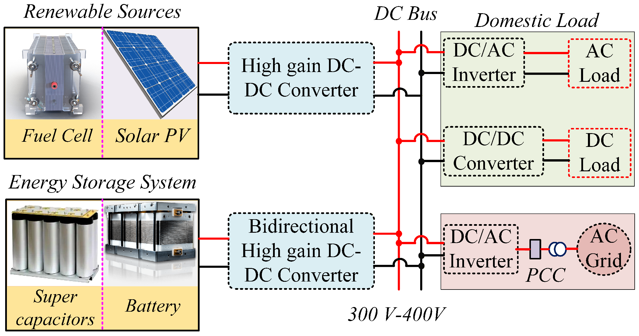
HIGH-GAIN dc-dc converters are essential for fuel cell and renewable energy systems designed for household applications [1,2]. A general layout of use of solar energy is shown in Figure 1. Photovoltaic energy source typically have low, erratic output voltages [3]. In renewable energy, a dc-dc converter required to control the output voltage level of renewable energy sources to match the demand of the utility [4,5]. For solar photovoltaic cell, two dc-dc converters are required for maximum power point tracking (MPPT) and boosting voltage. In various applications, multistage dc-dc converters are needed to meet high voltage demands. However, multistage power converters exhibit lower efficiency on account of higher power loss occurring in large number of components. In addition, multistage configurations increase the risk of failure and reduce the reliability of the system. The use of magnetic isolation between the input and output terminals determines whether high-gain dc-dc converters are classified as isolated or non-isolated [6]. A high-frequency transformer (HFT) is necessary for magnetic isolation, and because of the leakage inductance, it creates voltage spikes in power switches [7]. A non-isolated converter’s lack of magnetic isolation drastically lowers the converter’s size and cost.
In non-isolated converters, the conventional boost converter (CBC) is simple in operation and compact, but for high voltage gain it requires a high duty ratio [8]. However, at such a high duty ratio, voltage gain is influenced by semiconductor device parameters and the equivalent series resistance (ESR) of passive components (inductors and capacitors). Topologies derived from the CBC, such as cascaded boost converters, can achieve higher voltage while operating at low duty cycles [9,10]. Although these topologies have a large number of components, their efficiency decreases, leading to self-heating, which further reduces the reliability and lifespan of the converter. The literature discusses a variety of high-gain non-isolated dc-dc converters based on approaches such as the linked inductor [11], Z/quasi-Z network [12], switched capacitors (SC) network [13], and switched inductors (SL) network [14,15,16]. In order to attain high voltage gain, converters that use coupled inductors use the number of turn ratios as an extra degree of freedom. Nevertheless, excessive input current ripples, voltage spikes across the switch, and leakage inductance are linked to these converters. Clamped circuits are required to reduce the voltage spike, which raises the converter’s size and cost [11]. The voltage gain of the converter can have increased by using switched capacitor (SC) networks, and the gain increase is proportional to the number of SC networks used. Nevertheless, the issue related to SC circuits is high current transient, which increases the current stress on the switches. To mitigate the current transient, a small inductor is connected in series with the capacitor of SC network to obtain zero current switching (ZCS) but extra arrangement exhibits complex structure [10]. Multilevel boost converter (MBC) with SC is discussed in [17], but it requires a large inductor at the input to produce a steady input current. Reference [18] has reported input parallel output series with dual coupled inductor with reduced current ripple at input side. However, because the input inductors are connected to the voltage multiplier’s (VM) inductors, the converter’s switches have a high conduction current, which raises the conduction losses. An interleaved boost structure-based double-switch high-voltage gain converter with an N-stage Dickson (VM) is proposed in [19]. To obtain high voltage gain this converter require four VM-stages consisting of five diodes and five capacitors. Further by reducing the component modified Dickson charge pump VM with four diodes and five capacitors is presented in [20].
To increase the voltage gain with minimal switch voltage stress, ref. [21] makes use of an active switching inductor (ASL). Nevertheless, this converter’s diode voltage stress is more than the voltage of the output. The literature has since examined a number of hybrid topologies created by fusing ASL and SC networks [22,23,24,25,26]. To achieve high voltage gain, the authors of [22] combined the ASL network with an asymmetric ladder-SC network. Because of the low impedance, it experiences considerable current stress in the switches. To increase the voltage gain, a ladder SC network is combined with a regenerative-boost configuration and coupled with the ASL network in [23]. The regenerative-boost configuration greatly increases the size and expense of the converter by adding one switch and one inductor to the one shown in [22]. ASL-based converters with quadratic voltage gain are produced in [24] by connecting a diode-capacitor across the ASL network’s switch. This gives the switch a low-impedance path, which raises the inrush current significantly. Additionally, because of the asymmetrical structure of these converters, the switches and inductors experience unequal current stress, which raises the conduction losses. High voltage gain is typically achieved by integrating the SC and ASL networks. However, because of large SC networks, problems with current spikes in the diodes and switches are unavoidable. Furthermore, the output capacitance of the switches and the values of the inductor have a significant impact on ASL converters. Increased switch voltage stress and reduced efficiency result from the inductors creating a resonance circuit with the switches’ output capacitors while the switch is off [25]. A hybrid converter that combines an ASL network with a quasi-Z-source network is suggested in [27]. This converter’s limited duty cycle is a disadvantage, despite the fact that it generates a much higher voltage gain. Any change in the duty cycle value greatly affects converters with small duty cycle ranges [28].
In [29], a unidirectional switch is included into the ASL network to provide a triple switch, triple mode (TSTM) dc-dc converter. The voltage gain is increased by this converter’s two duty cycles ( D 1 and D 2 ). Additionally, it improves overall efficiency by providing flexibility in output voltage management through various duty cycle combinations. To increase voltage gain, SC networks and voltage lift cells are used. Voltage raise cells are added to the TSTM converter at the input terminals in [30,31], increasing the current strains in the switches. Furthermore, in converters, the output voltage is not as high as the voltage stress on the output diode and unidirectional switch [29,30,31].
By substituting a passive switched inductor network for the ASL network’s simple inductors, voltage gain is increased in [32,33]. However, the increasing number of diodes and inductors makes these converters large. Three control strategies for hybrid TSTM converters are examined in [34] for their flexibility: (1) manipulating D 1 and fixing D 2 , (2) fixed D 1 and regulating D 2 , and (3) controlling both D 1 and D 2 . On the other hand, TSTM converters [14,29,30,31,32,33,35,36] shows the absence of common ground between the input and output which eventually led to issues related to the electromagnetic interference, leakage current, etc. All these converters also show the oscillations during mismatch of inductance which increases the voltage stress across the switches. Because of this, power dissipation in semiconductor devices and passive components are increased, leading to a self-heating effect in the converter, causing temperature-dependent parameter variations (such as ESR of passive components, on-state mosfet resistance, forward voltage drop of diodes, etc.) to vary repeatedly, which increases the thermal stress on the converter devices and significantly reduces the efficiency, voltage gain, and reliability of the converter [37,38,39].
This article proposes a unique TSTM dc-dc converter that achieves significant voltage gain by combining ASL and SC networks for household electrification. The following is a summary of the suggested converter’s features.
  • Two capacitors are separated from the output capacitor. When switched off, each capacitor provides a single ASL network switch. As a result, the voltage stress across the switches is decreased and the voltage oscillation is abolished.
  • The proposed converter operates with two duty cycles ( D 1 , D 2 ) and offers the flexibility to achieve the desired voltage gain with different combinations of duty cycles. The operational efficiency of the converter can be improved by properly selecting the duty cycles for a given voltage gain.
  • The proposed converter has three controller design degrees of freedom, including the following options: (1) regulating D 1 and repairing D 2 , (2) repairing D 1 and regulating D 2 , and (3) regulating both D 1 and D 2 .
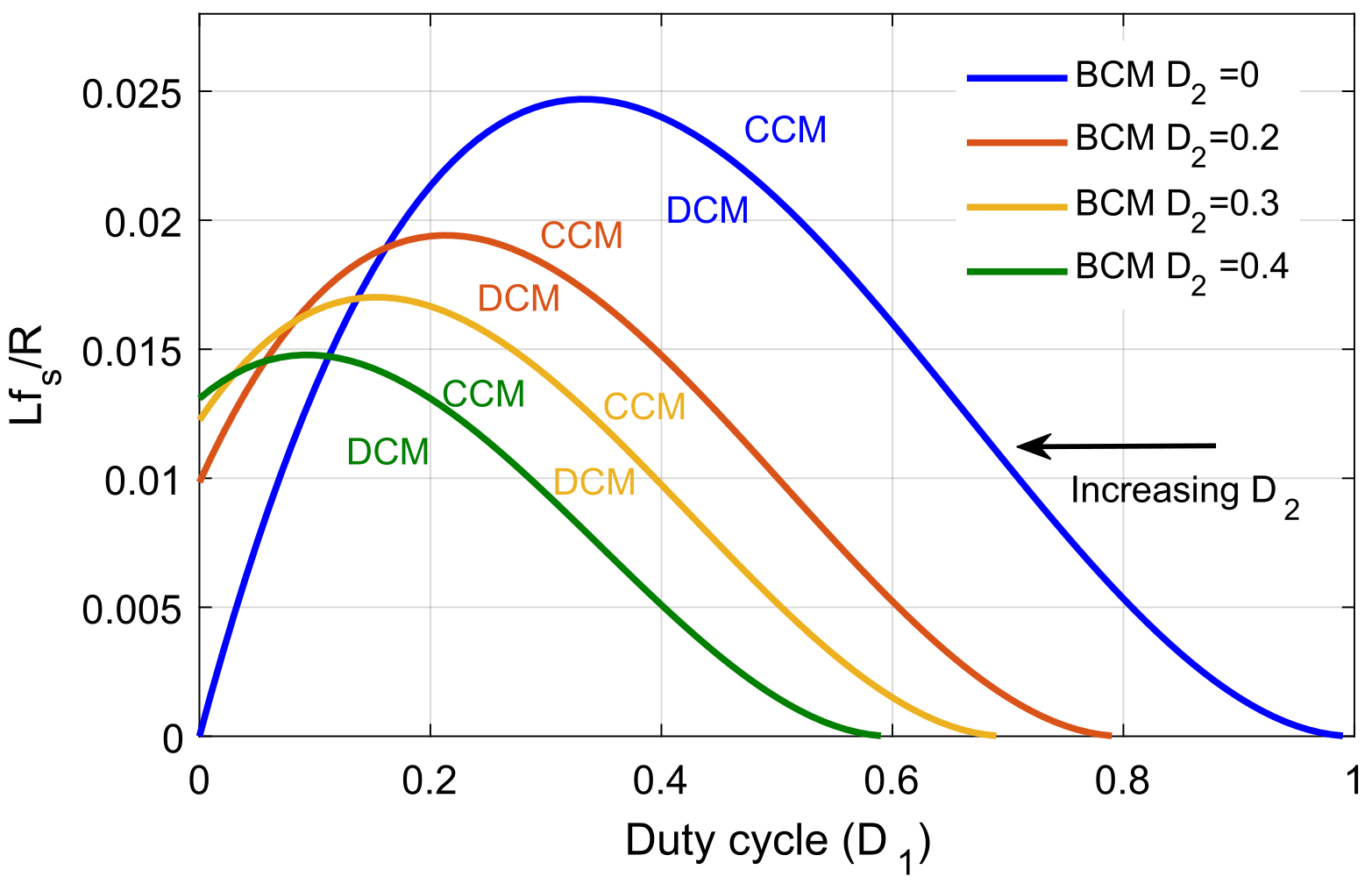
  • The proposed converter offers a common grounding feature between input and output to eliminate the electromagnetic interference (EMI) and leakage current issues. Furthermore, depending on the value of D 2 , it has different boundaries for continuous conduction modes (CCM) and discontinuous conduction modes (DCM).
  • The suggested converter provides significant voltage gain across a broad range of duty cycles by utilizing ASL and SC networks. This converter is less sensitive to any change in the duty cycle value than converters with limited duty cycles.

2. Configuration of High Gain Converter

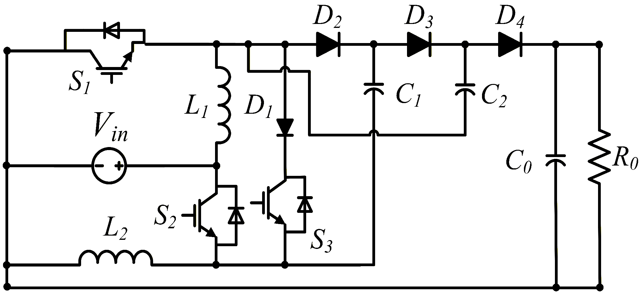
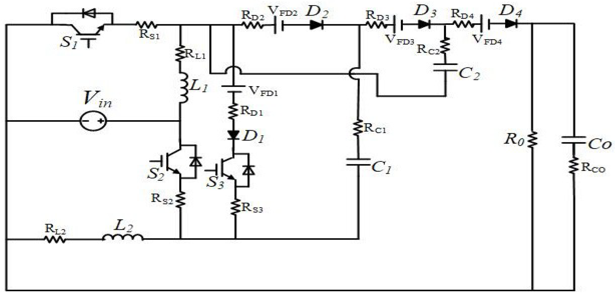
The proposed converter is composed of two switches S 1 , S 2 that act as a main switch and two inductors L 1 , L 2 at the low voltage side, as shown in Figure 2. In addition to this one auxiliary switch S 3 is connected in series with diode D 1 . SC cell ( D 2 C 1 ), ( D 3 C 2 ) and ( D 4 C 0 ) are utilized in converter to enhance the voltage gain of converter. The duty cycle of of main and auxiliary switch is defined by D 1 and D 2 respectively. In this section the detailed analysis of developed converter is discussed in details. For this some assumptions are considered:
  • Parasitic effects on devices are ignored.
  • Capacitor are enough to suppress the voltage ripple.
  • Inductance values at low voltage side are equal ( L 1 = L 2 ).

2.1. CCM Operation

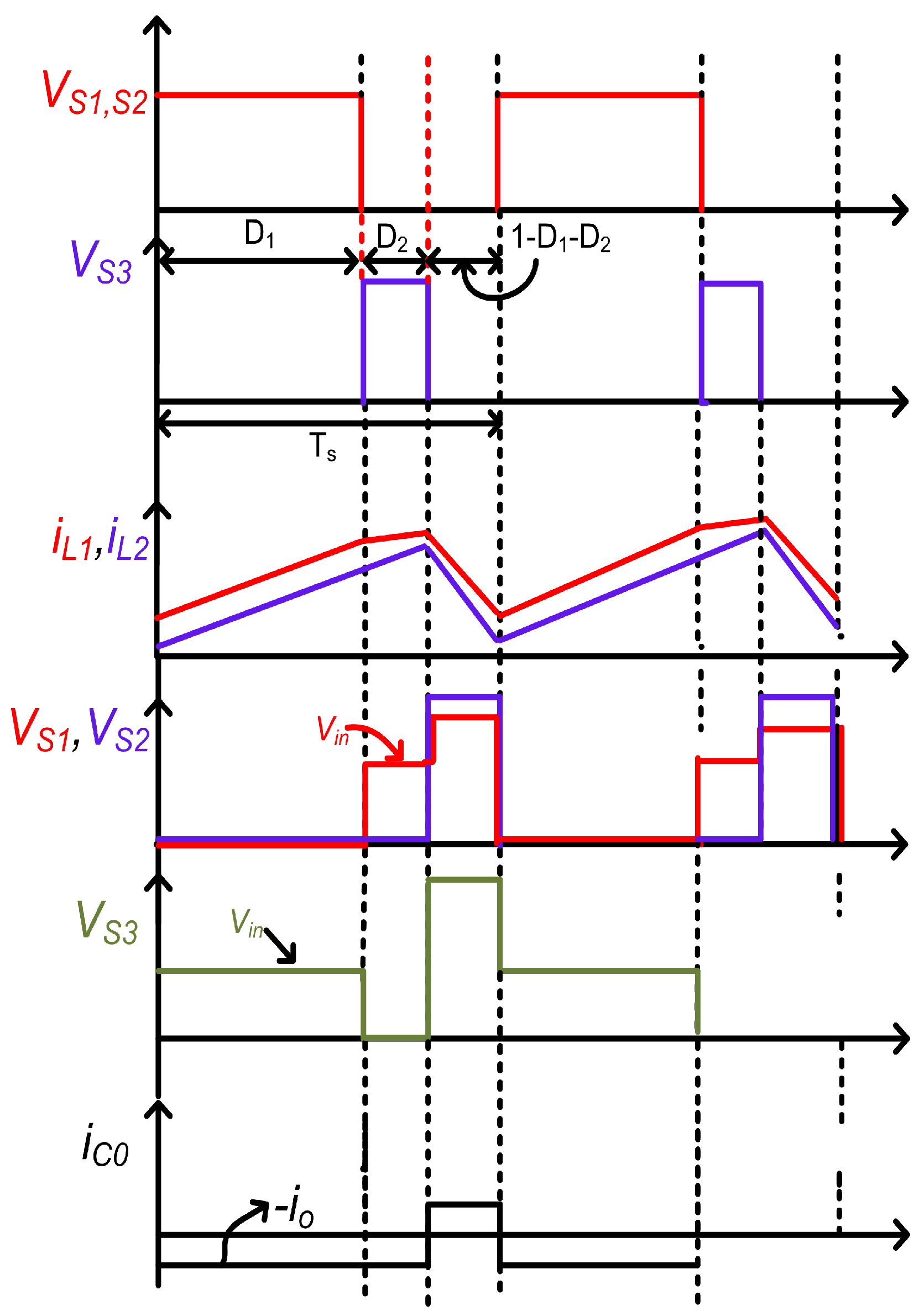
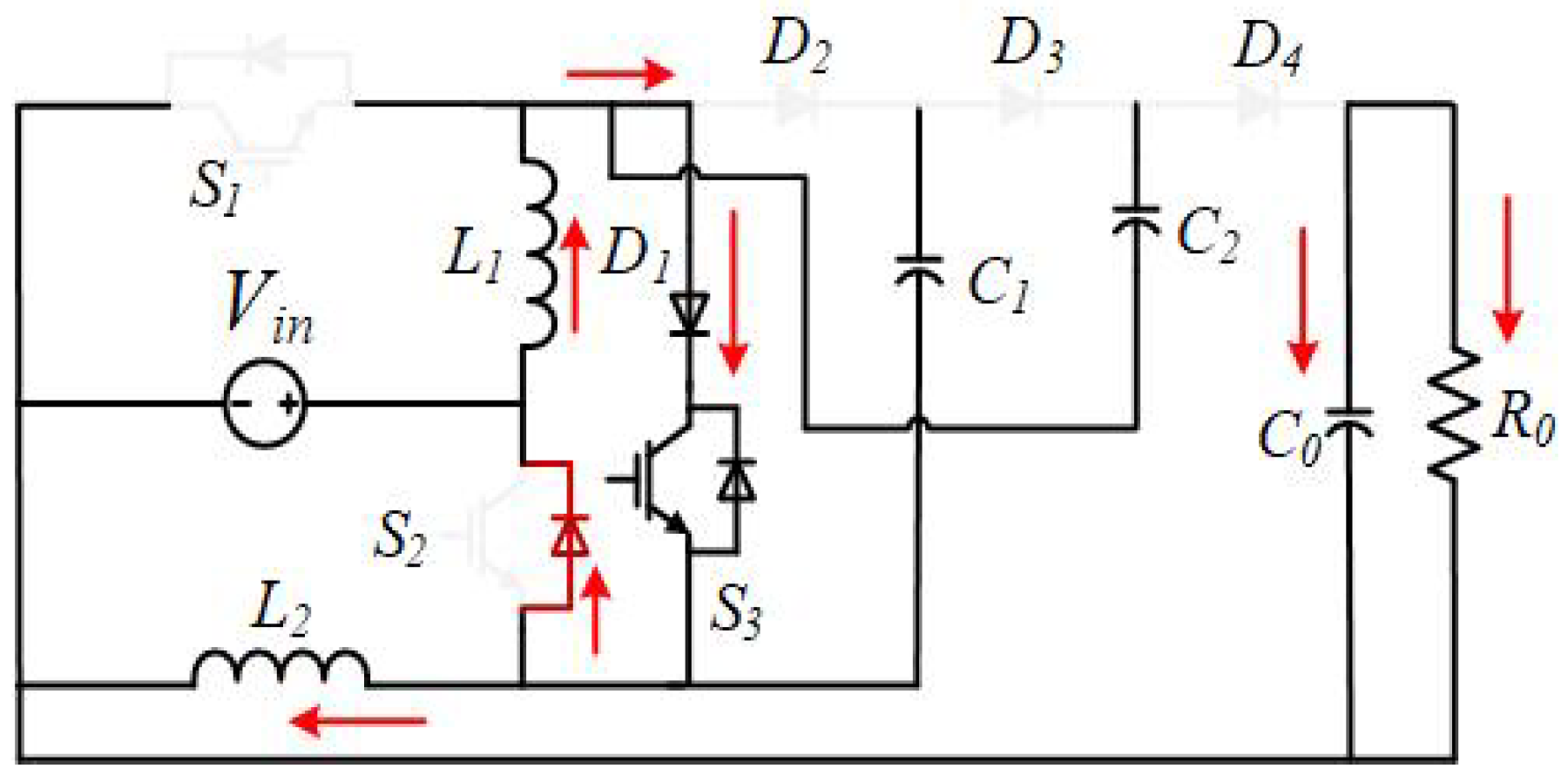
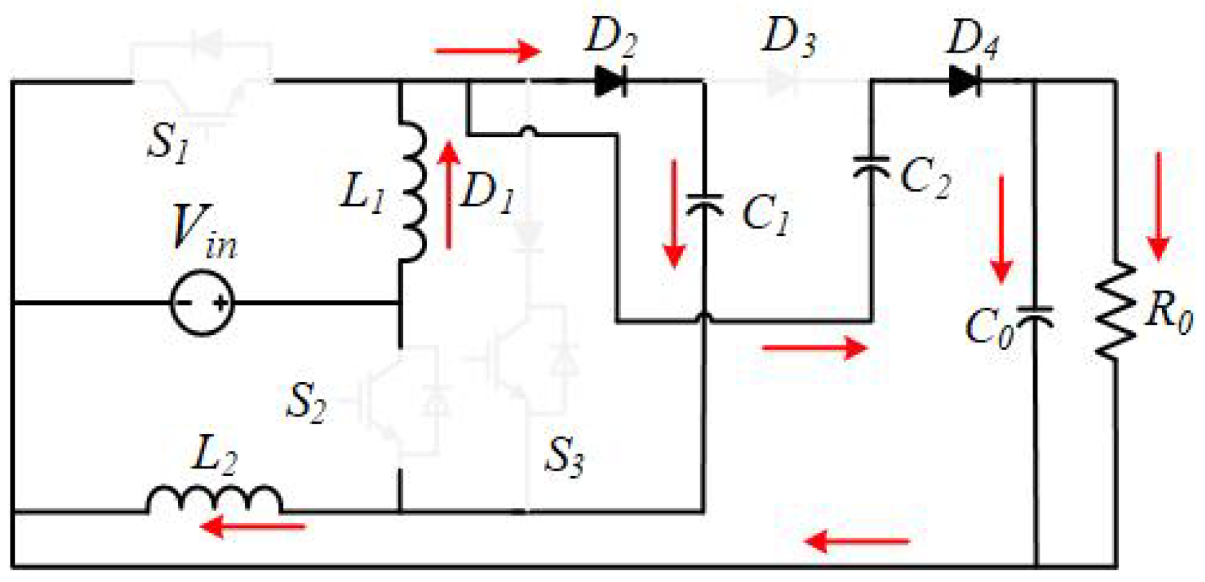
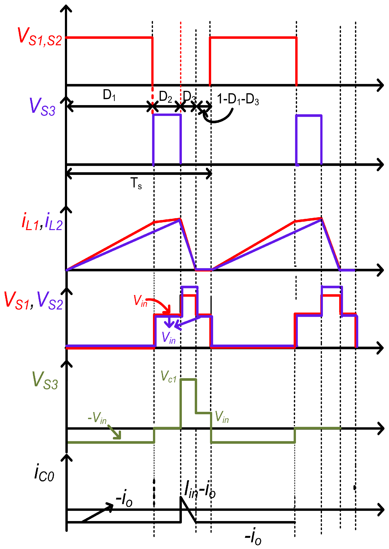
The proposed converter has three modes in CCM, which can be summarized as follows. The steady state waveform during CCM mode is shown in Figure 3. The conducting and nonconducting devices are shown by red and dashed color, respectively, along with the direction of the current path.

2.1.1. Mode-1 ( 0 < t < D 1 T s )

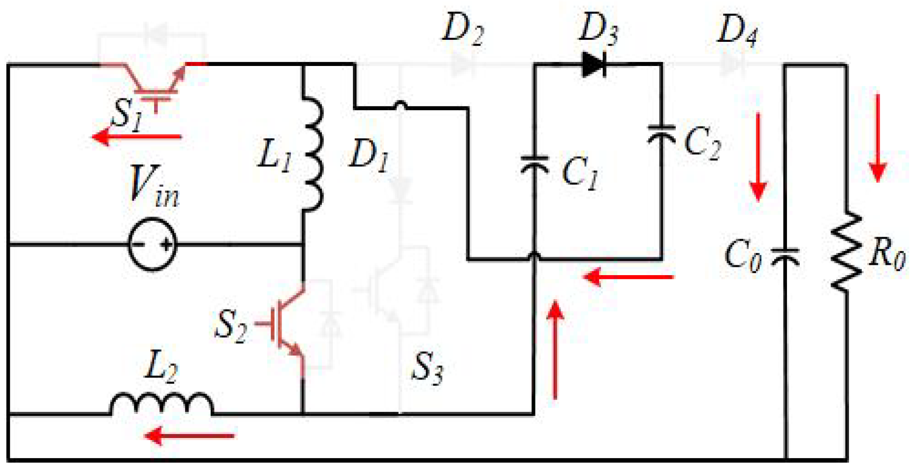
For this mode as shown in Figure 4, main switches S 1 , S 2 are turned ON and auxiliary switch S 3 is turned OFF. Both inductors L 1 and L 2 are magnetized by input voltage V i n . Capacitor C 1 discharges its energy to charge C 2 through diode D 3 . The voltage across capacitors and inductors is obtained as follows using equivalent circuit:
V L 1 = V L 2 = V i n V C 2 V C 1 = V i n }

2.1.2. Mode-2 ( D 1 T s < t < D 2 T s )

Both switches S 1 and S 2 are turned OFF, but auxiliary switch S 3 is turned ON as shown in Figure 5. The voltage across inductor L 1 is almost zero due to the reverse conducting diode of switch S 2 . However, inductor L 2 is still magnetized with V i n .
V L 1 = 0 V L 2 = V i n }

2.1.3. Mode-3 ( D 2 T s < t < T s )

In this mode all three switches are turned OFF as shown in Figure 6. Inductor L 1 releases its stored energy to charge capacitor C 0 via diode D 4 . Similarly, L 2 releases its energy to charge capacitor C 1 through diode D 2 . The following equation holds for this mode:
V L 1 = V i n + V C 2 V 0 V L 2 = V i n V L 1 V C 1 V L 2 = V 0 V C 1 V C 2 }
The relationship between output and input voltage depends on duty cycles D 1 and D 2 , which can be derived using the volt-second principle across both inductors L X (X = 1, 2).
0 D 1 T s V L X d t + D 1 T s D 2 T s V L X d t + D 2 T s T s V L X d t = 0
Substituting the value of V L 1 and V L 2 , results following expressions,
V C 1 = ( 1 + D 1 ) ( 1 D 1 D 2 ) V i n V C 2 = ( 2 D 2 ) ( 1 D 1 D 2 ) V i n }
Therefore, the output voltage of converter is
V 0 = ( 3 2 D 2 ) ( 1 D 1 D 2 ) V i n
Voltage gain M C C M of proposed converter can be given by
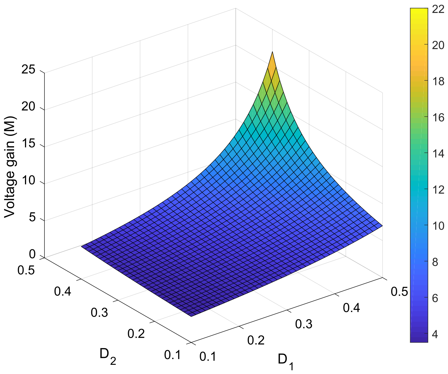
M = V 0 V i n = ( 3 2 D 2 ) ( 1 D 1 D 2 )
The voltage gain variation of proposed converter is illustrated in Figure 7.

2.2. DCM Operation and Boundary Condition

In DCM operation is divided into four operating modes shown in Figure 8. The first and second operational modes are the same as the CCM operation. The inductors current reaches to zero in third operating modes ( D 3 ) and in final fourth mode all devices are turned OFF and inductor current becomes zero. Therefore, in DCM operation following relation can be derived.
V i n D 1 + V i n D 2 + ( V 0 V C 1 V C 2 ) D 3 + 0 = 0 D 3 = ( D 1 + D 2 ) ( V C 1 + V C 2 V 0 ) V i n }
The capacitor discharges its stored energy to load. The average current in the output capacitor for every switching state is given by,
I C 0 = 1 2 ( D 3 T s I L 2 m a x ) I 0 T s T s
In steady state I C O equals to zero,
I C 0 = ( D 1 + D 2 ) 2 V i n 2 T s ( V C 1 + V C 2 V 0 ) 2 L V 0 R = 0
Solving (10) voltage gain in DCM mode of operation is given by,
V 0 V i n = 1 2 A + 1 2 A 2 + 2 ( D 1 + 0.5 D 2 ) 2 τ
where, τ = L R T s and A = 3 + D 1 D 2 1 D 1 D 2
The boundary condition for the developed converter can be found as:
τ B C M = ( 1 D 1 D 2 ) 2 ( D 1 + 0.5 D 2 ) 2 ( 3 2 D 2 )
However, for the converter’s CCM mode operation, the (13) is necessary to be satisfied.
τ > ( 1 D 1 D 2 ) 2 ( D 1 + 0.5 D 2 ) 2 ( 3 2 D 2 )
The boundary condition of the proposed converter for different value of D 2 is shown in Figure 9.

2.3. Effect of Parasitic Parameter on Voltage Gain

To show the effect of parasitic parameters on the voltage gain, the following parasitic parameters are considered: R L 1 —Inductor L 1 resistance, R L 2 —Inductor L 2 resistance, R S 1 —Switch S 1 resistance, R S 2 —Switch S 2 resistance, R D 1 —Diode D 1 resistance, R D 2 —Diode D 2 resistance, R D 3 —Diode D 3 resistance, R D 4 —Diode D 4 resistance, R C 1 —Capacitance C 1 resistance, R C 2 —Capacitance C 2 resistance, R C 0 —Capacitance C 0 resistance, V F D 1 —Diode D 1 forward voltage drop, V F D 2 —Diode D 2 forward voltage drop, V F D 3 —Diode D 3 forward voltage drop, V F D 4 —Diode D 4 forward voltage drop as shown in Figure 10.
The voltage equation in Mode-1 ( 0 < t < D 1 T s ) is
  V L 1 = V i I L 1 R L 1 I s 1 R s 1   V L 2 = V i I L 2 R L 2 I s 2 R s 2   V c 2 V c 1 = V i V D F 3 I s 1 R s 1 I s 2 R s 2   + I c 1 , 1 ( R c 1 + R c 2 + R D 3 ) }
The voltage equation in Mode-2 ( D 1 T s < t < D 2 T s ) is
  V L 1 = I L 1 ( R L 1 + R D 1 + R S 1 ) V D F 1   V L 2 = V i I L 2 R L 2 }
The voltage equation in Mode-3 ( D 1 T s < t < T s ) is
  V L 1 = V i I L 1 R L 1 + I c 2 , 3 R c 2 V c 2 I D 4 R D 4 V D F 4 V 0 I c 0 , 3 R C 0   V L 2 = V i V L 1 I L 1 R L 1 I D 2 R D 2 V D 2 V c 1 I c 1 , 3 R c 1 I L 2 R L 2 }
Applying voltage second balance in Equation (14), (15), and (16),
G = 3 2 D 2 1 D 1 D 2 α D 1 + β D 2 V i ( 1 D 1 D 2 ) 2 γ + ζ V i   2 V D F 1 + 2 V D F 2 + ( 1 D 1 D 2 ) V D F 3 V i ( 1 D 1 D 2 ) }
where, α = 2 I L 1 R L 1 + 2 I S 1 R S 1 + I L 2 R L 2 + I S 2 R S 2 , β = I L 2 R L 2 + 2 I L 1 ( R L 1 + R D 1 + R S 3 ) , γ = 2 I L 1 R L 1 + 2 I L 2 ( R L 2 + R D 2 + R C 1 ) and ζ = I S 2 R S 2 + I S 1 R S 1 + I C 1 , 1 ( R C 1 R C 2 R D 3 )

3. Device Stress and Design Equations

3.1. Voltage and Current Stress Across Diode and Switches

Applying Kirchhoff’s current law (KCL) in Figure 4, Figure 5 and Figure 6, current stress through capacitor, diodes and switches can be derived as reported in Table 1.
Similarly like current stress voltage stress across diodes and switches can be examined in Table 2.

3.2. Inductor and Capacitor Design

For the developed converter to operate in CCM mode the inductor current must be higher than half of their ripple current ( 2 I L x Δ i L , x = 1 , 2 ) . The average current flowing through both inductor is given as:
I L 1 = 2 I 0 ( 1 D 1 D 2 ) ,   I L 2 = I 0 ( 1 D 1 D 2 ) }
The inductance can be calculated as:
L 1 V i n 2 ( 3 2 D 2 ) D 1 4 P 0 f s ,   L 2 V i n 2 ( 3 2 D 2 ) D 1 2 P 0 f s }
The capacitance selection is based on voltage ripple in the capacitors or is 1% of their voltage.
C 1 = C 2 = I 0 Δ v c 1 f s ,   C 0 = I 0 D 1 Δ v c 0 f s }
where Δ v c 1 %, Δ v c 2 % and Δ v c 0 are the percentage voltage ripple and f s = switching frequency of converter.

3.3. Voltage Balancing Across the Switches

In [40], the voltage oscillation across switches of ASI converter has been studied. This oscillation is present due to unequal values of either (i) drain to source capacitors of ( C s 1 & C s 2 ) MOSFETs or (ii) inductances ( L 1 & L 2 ) or both. In several ASI converters, this oscillation have been observed. Thus, the voltage stress of the switches is practically higher than the theoretical one. In the proposed converter, voltage across C s 1 & C s 2 are supported by the capacitors voltage of the SC cells. Subsequently, the voltage oscillation across C s 1 & C s 2 are suppressed. Subsequently, the practical MOSFETs’ voltage stress is reduced. Analytical proof of suppression of voltage stress is as follows:
From Figure 4 and Figure 5, the voltages across C s 1 and C s 2 are obtained as
V C S 1 = V S 1 = V o V C 2
and,
V C S 2 = V S 2 = V i + V C 1 + V C 2 V o
V i , V C 1 , V C 2 & V o are constant and therefore, V S 1 and V S 2 are also constant. Therefore, even if the MOSFETs internal capacitance is different for two MOSFETs then also the voltage across the MOSFETs i.e., V C S 1 and V C S 2 remain constant. Hence, the voltage oscillations across the MOSFETs are suppressed.
According to Figure 4, the charging voltage of L 1 and L 2 are equal, and the principle of energy balance ensures equal discharging voltage across these inductors. V L 1 , V L 2 are obtained as
V L 1 = V i n + V C 2 V 0 , V L 2 = V 0 V C 1 V C 2
Therefore, v L 1 and v L 2 are also constant and therefore, mismatch in the inductance parasitic does not create any oscillation. This analysis shows the voltage across the switches is reduced due absence of oscillation which felicitate us to use lower rating switches and hence efficiency will be improved.

4. Comparison, Analysis and Dynamic Model of Converter

4.1. Comparison with Other Topologies

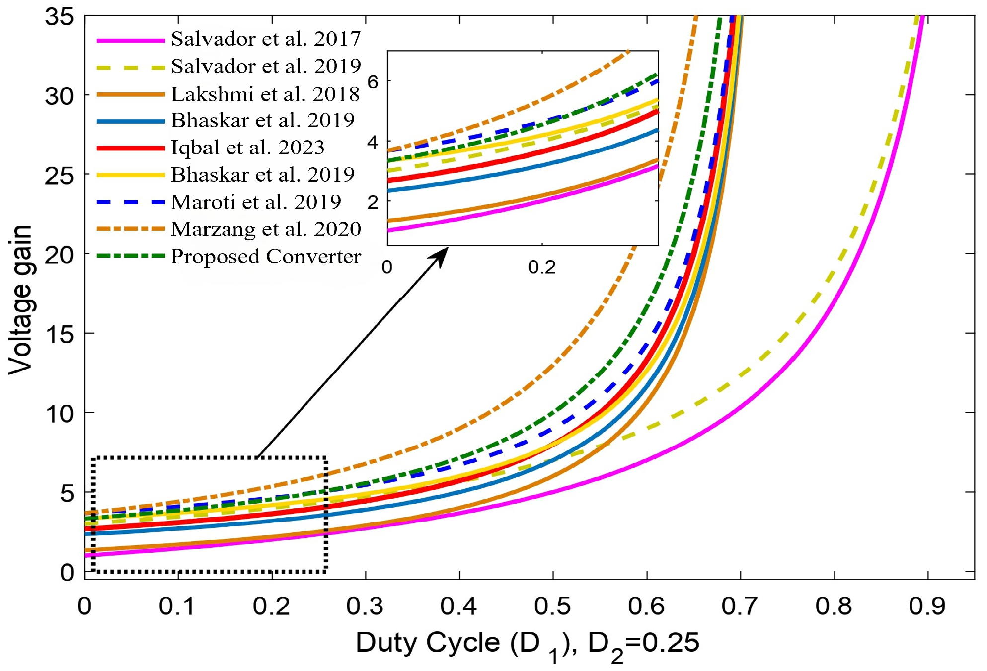
In order to clearly demonstrate the benefits of the proposed converter, Table 3 compares similar topologies in terms of voltage gain, number of devices utilized and switch as well as diode stress. The ASL network in converter [41,42] needs a high duty cycle to achieve a higher voltage conversion ratio. A three switch-based ASL converter is reported in [29] with low component to achieve high gain; however, the voltage stress across the auxiliary switch is equal to the output voltage. An improved version of the converter is presented in [32] with more switch stress across the auxiliary switch. Converter [31] achieves high gain but all switches are under high voltage stress compared to the proposed converter. Converter [30,33] is reported earlier with a slightly low gain and the output diode has greater voltage stress. The authors report a converter [34] with greater gain compared to the proposed converter, but the output diode is having greater voltage stress. All compared converters reported earlier, presented in Figure 11, do not have the feature of common ground except the proposed converter, which helps in reducing the electro magnetic interference and leakage current issues in the proposed converter.
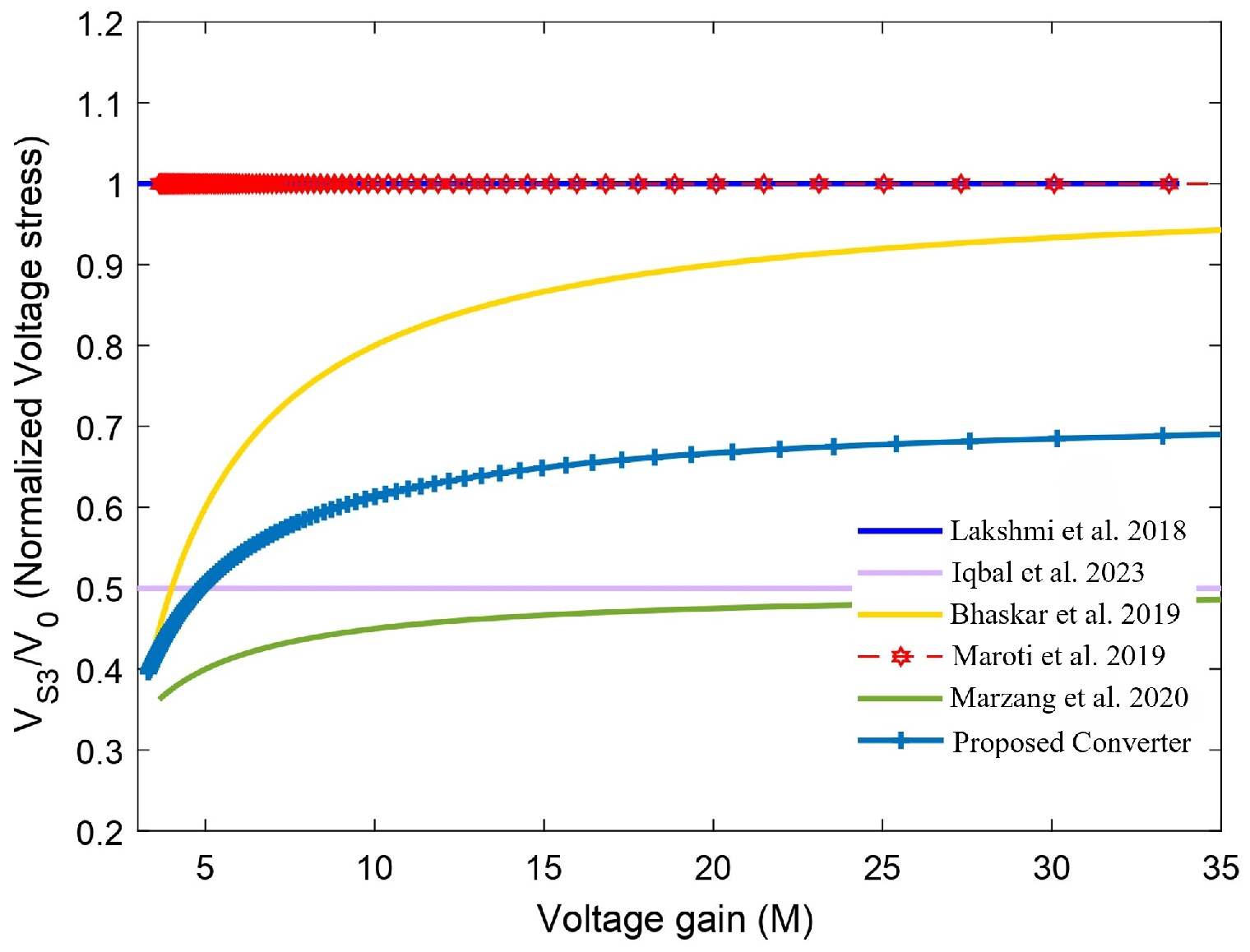
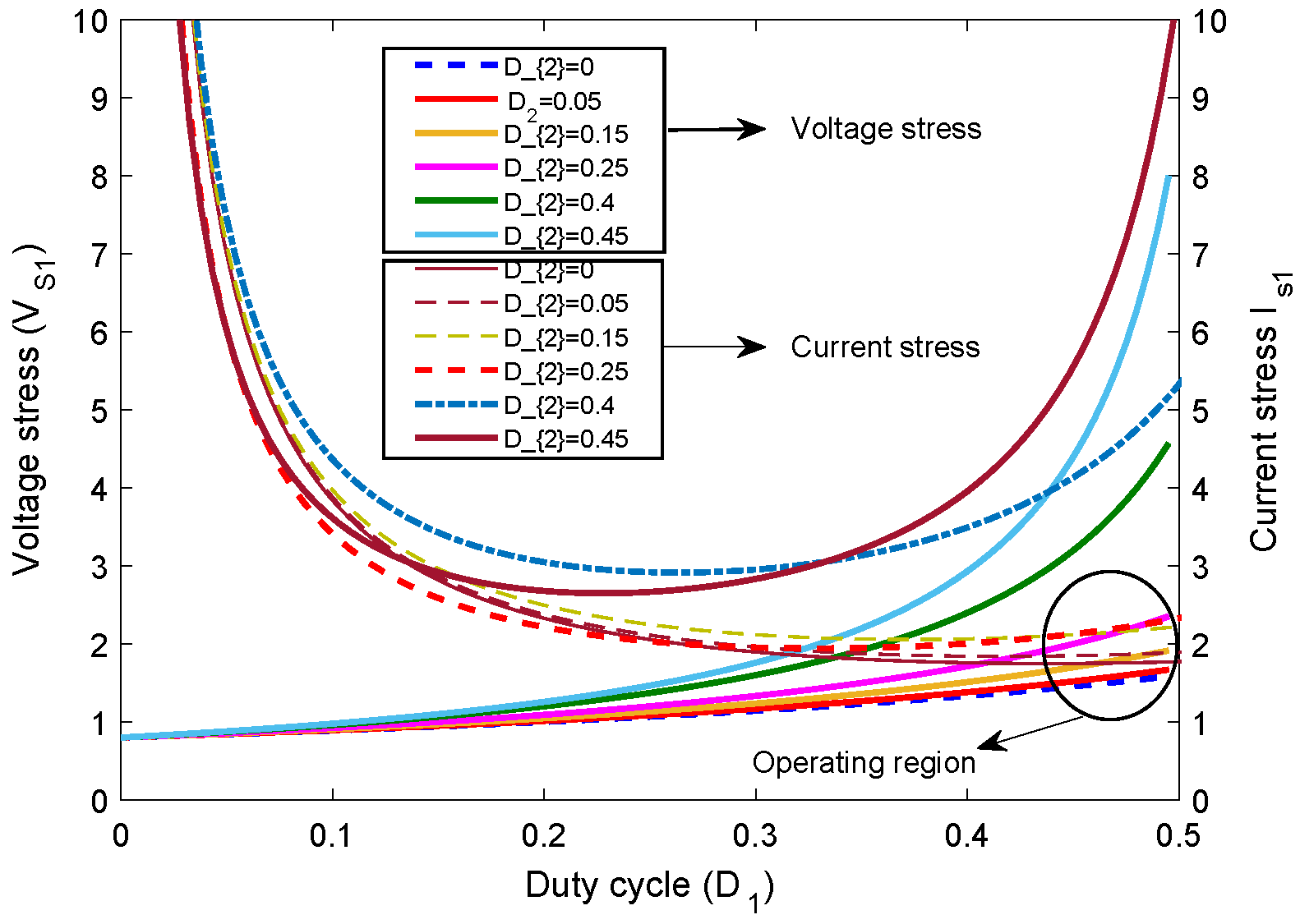
Normalized voltage across auxiliary switch S 3 is illustrated in Figure 12. It can be seen that the voltage across switch S 3 is in the acceptable range with respect to other structures. Similarly the voltage and current stress of the switch is shown in Figure 13 for different value of D 2 . It can be seen that the optimal value of voltage and current stress for switch is near to D 1 = 0.45 0.5 and D 2 = 0.15 0.3 . Based on the above analysis, we designed converter for D 1 = 0.5 and D 2 = 0.25 to achieve the desired gain with minimal device stress. Furthermore, the proposed converter stored energy in inductor and capacitor is lower when compared to other converters as shown in Table 4, which signifies the improved power density. Moreover, the switch and diode utilization is better in the proposed converter which also addresses the concern of high cost. The cost of the proposed converter is lowest amongst other converters.

4.2. Dynamic Modeling

In order to control the developed converter, dynamic modelling of the converter is derived using a small-signal AC model which helps to analyze its stability. For controlling the output voltage here we control duty D 1 and fixed duty D 2 . Two inductor currents ( i ^ L 1 i ^ L 2 ) and two capacitor voltages ( v ^ c 1 , v ^ c 2 and v ^ c 0 ) are taken as state variables. For all three operating modes of the converter, a set of equations is obtained for each period. The coupling between capacitors C 1 and C 2 has been eliminated by adding the corresponding series resistance ( r C 2 ) within the same loop to prevent the incorrect state variables.
i L 1 ( t ) = I L 1 + i ^ L 1 ( t )   i L 2 ( t ) = I L 2 + i ^ L 2 ( t ) v C 1 ( t ) = V C 1 + v ^ c 1 ( t )   v C 2 ( t ) = V C 2 + v ^ c 2 ( t ) v C 0 ( t ) = V C 0 + v ^ c 0 ( t )   v i n ( t ) = V i n + v ^ i n ( t ) d 1 ( t ) = D 1 + d ^ 1 ( t )     }
The state, input, output, and control variables can be characterised by small-signal disturbances Equation (24). Where I L 1 , I L 2 , V C 1 , V C 2 , V C 0 , V i n and D 1 are the steady state components, i ^ L 1 ( t ) , i ^ L 2 ( t ) , v ^ c 1 ( t ) , v ^ c 2 ( t ) , v ^ c 0 ( t ) , and d ^ 1 ( t ) are the small-signal disturbances.
G v d 1 ( s ) = v 0 ^ ( s ) d ^ 1 ( s ) = 2.94 × 10 6 s 4 3.67 × 10 13 s 3 3.0 × 10 27 s 2 8.9 × 10 20 s + 1 × 10 25 8.7 s 5 + 1.08 × 10 8 s 4 + 1.81 × 10 10 s 3 + 4.78 × 10 15 s 2 + 4.18 × 10 17 s + 5.19 × 10 21
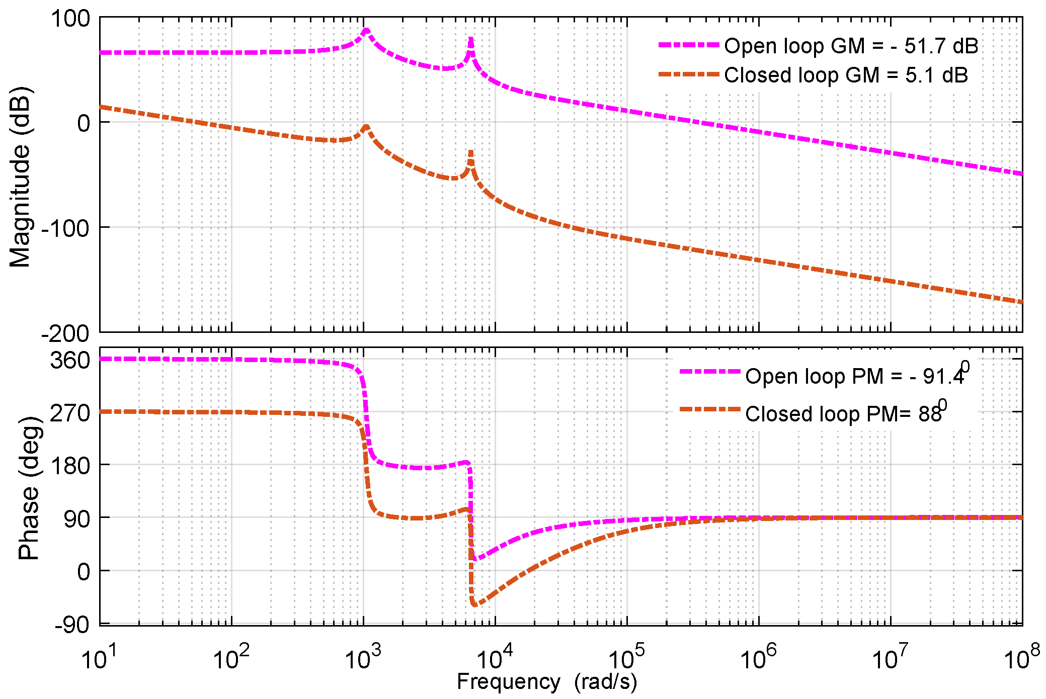
After perturbation and linearisation, the proposed converter’s transfer function is obtained as Equation (25). From the transfer function demonstrated in Equation (25), the Bode plot for the proposed converter is obtained as shown in Figure 14. The Bode plot shows that the gain margin (GM) and phase margin (PM) are negative, which indicates that the proposed converter is unstable in open-loop operation.
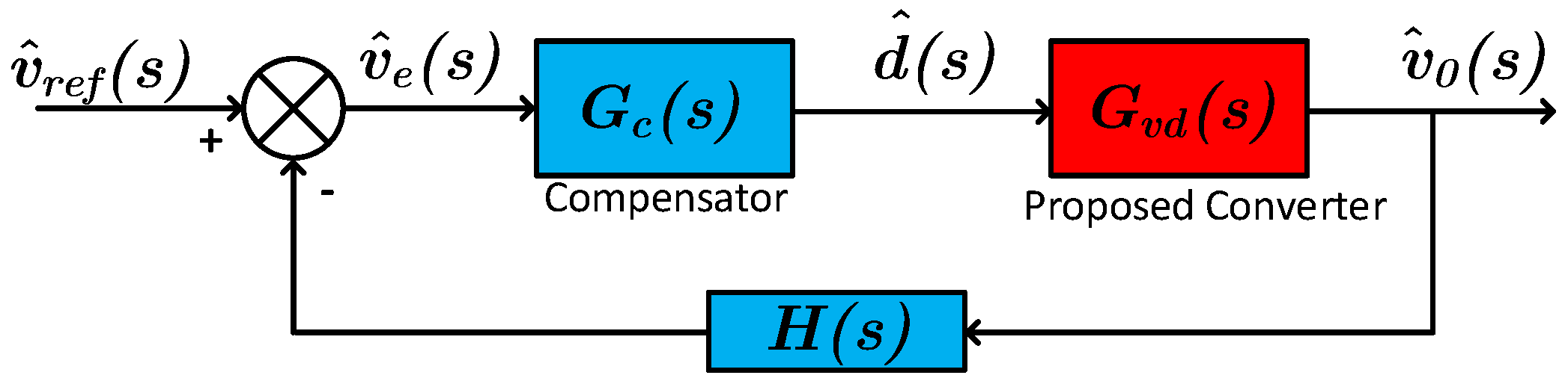
In order to stabilize the converter, a controller is required as shown in Figure 15. Here, a single loop based voltage control technique using a proportional integral (PI) is employed to regulate the output voltage of the developed converter. The behaviour of the converter is shown in Figure 15, after placing a controller and both GM and PM are positive suggests that the converter has stabilized.

5. Experimental Result and Its Analysis

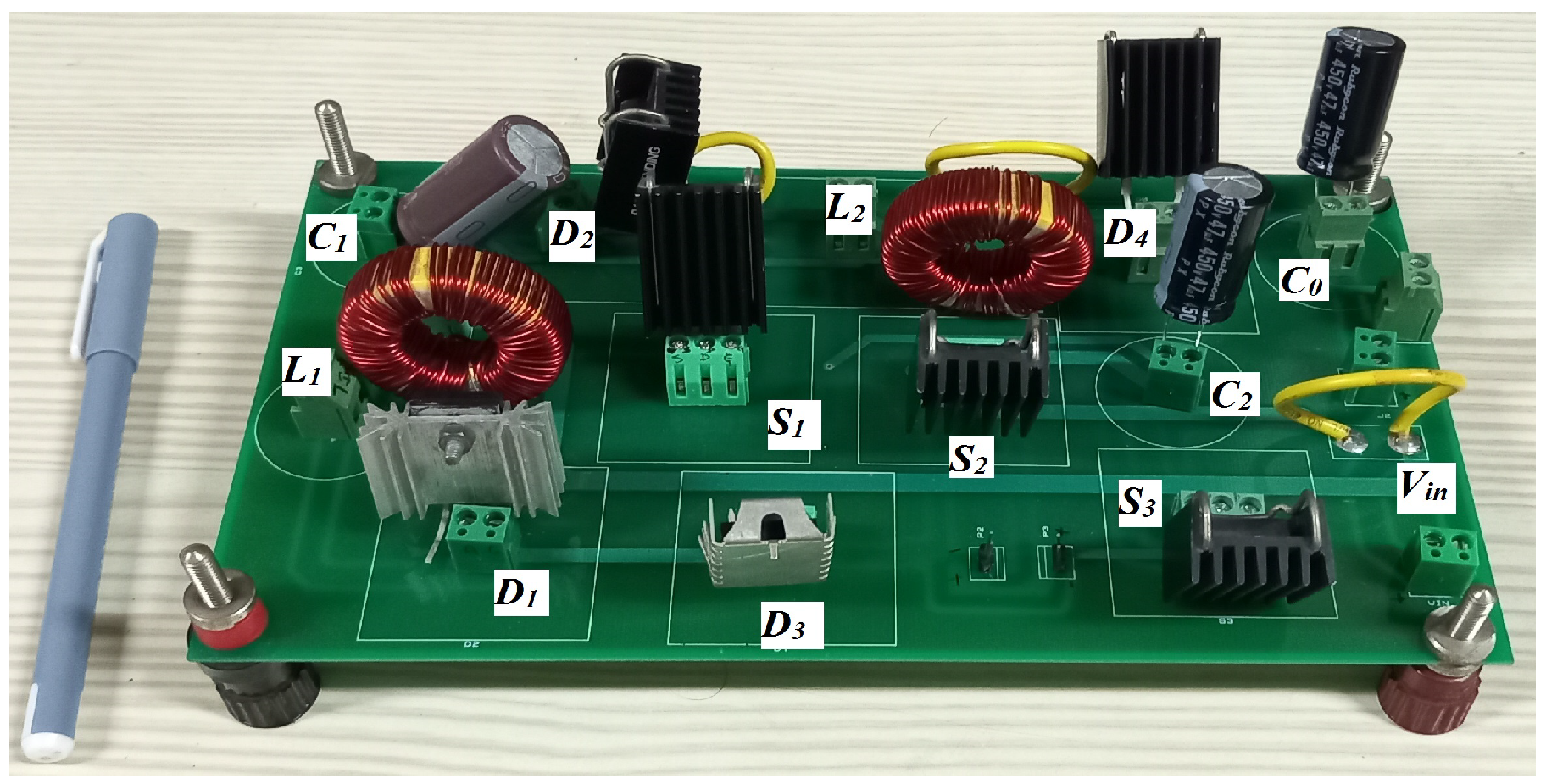
To validate the theoretical analysis, a laboratory prototype of the converter with 400 W output power has been built; a photograph of the prototype is shown in Figure 16 and the specifications of the converter parameters and comparison between measured and calculated values are in Table 5 and Table 6, respectively. All measurements of the converter parameters have been taken using the Yokogawa DLM2024 (200 MHz) oscilloscope, the Hioki-3273-50 clamp ON (30 A, 0.1 V/A) current probe, and the HIOKI differential 9322 voltage probe.
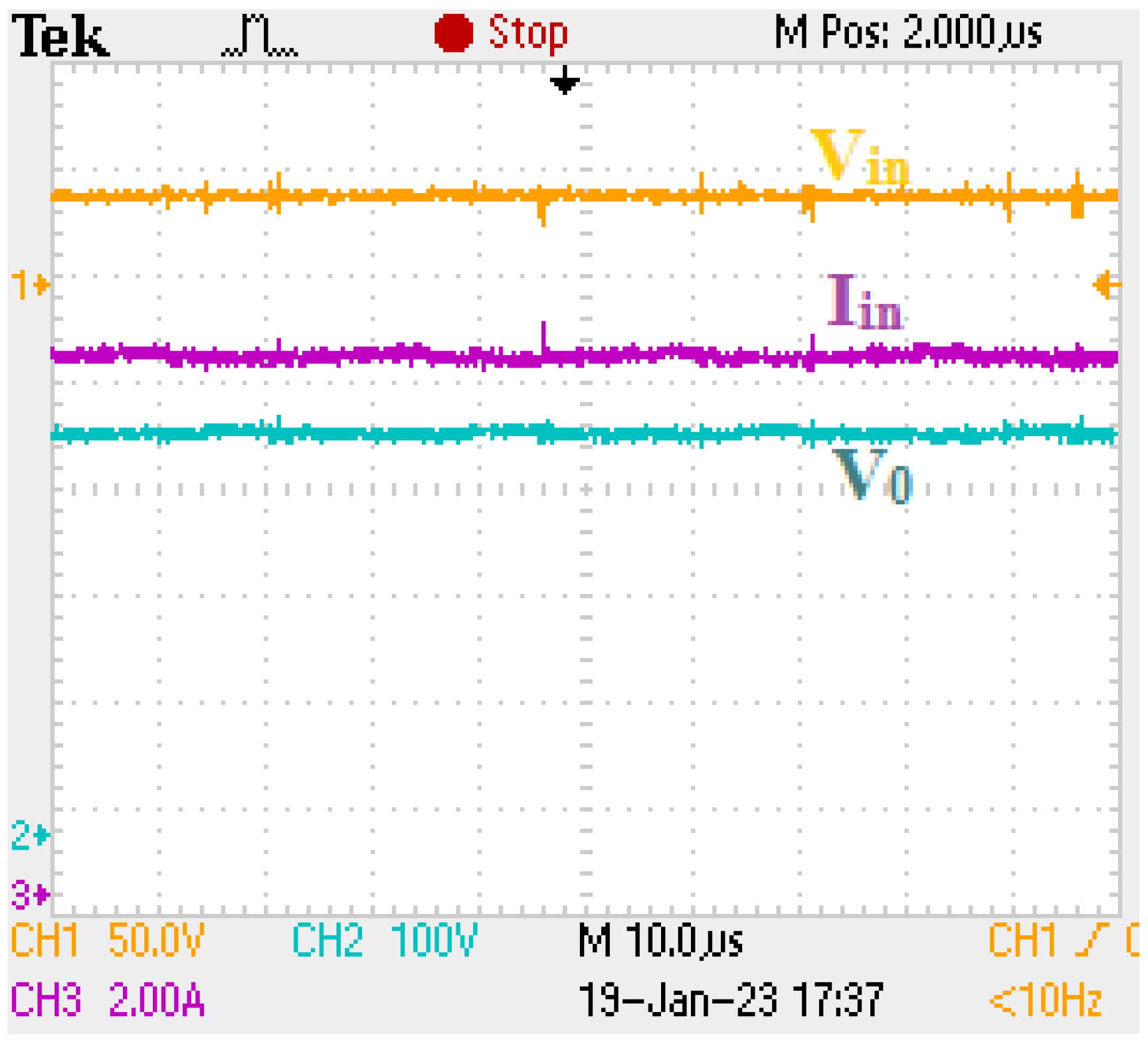
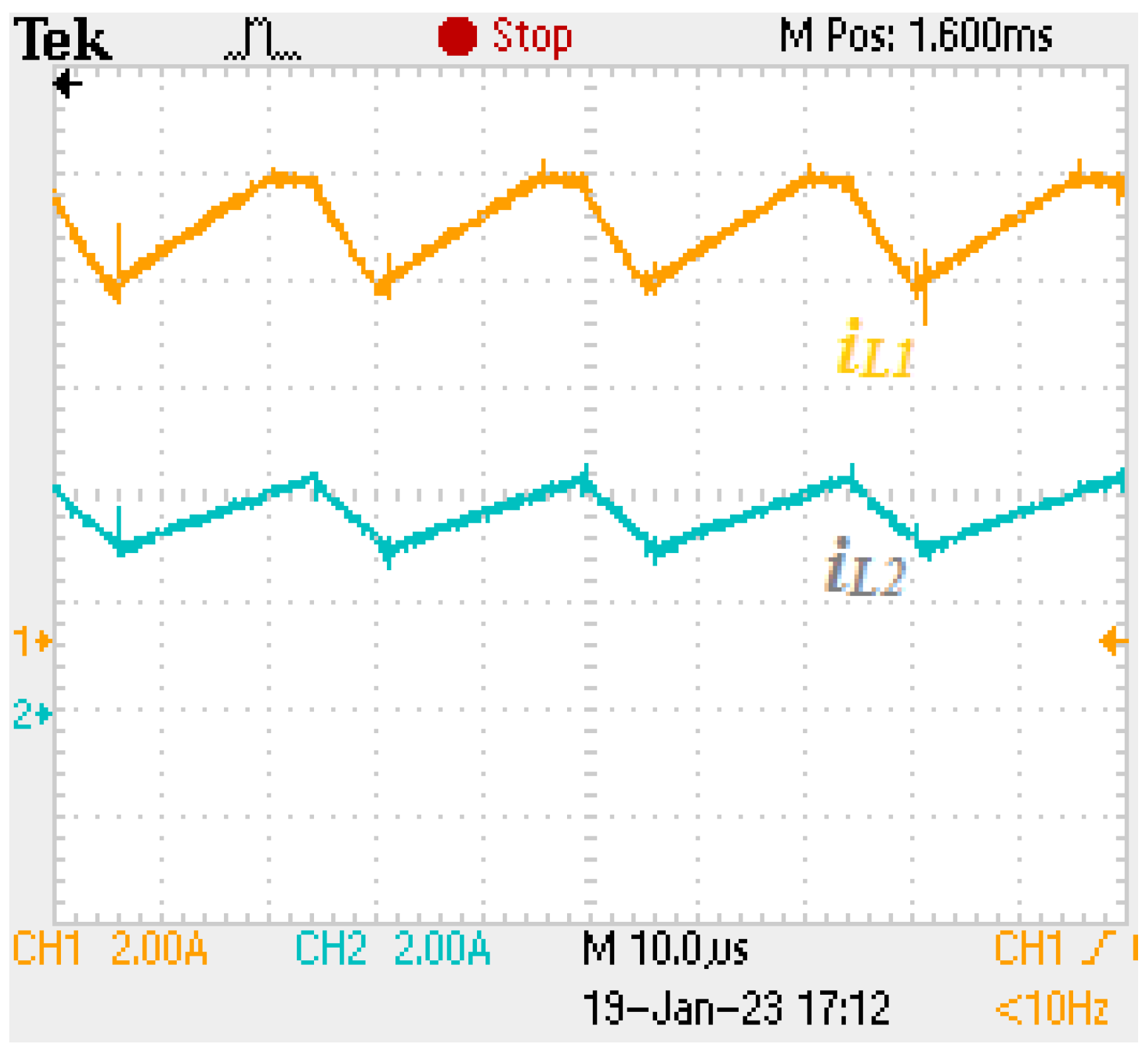
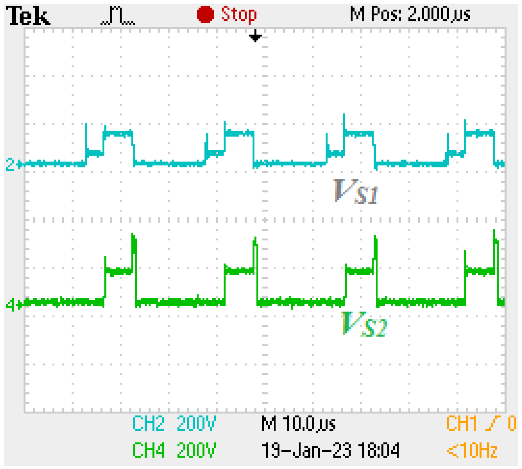
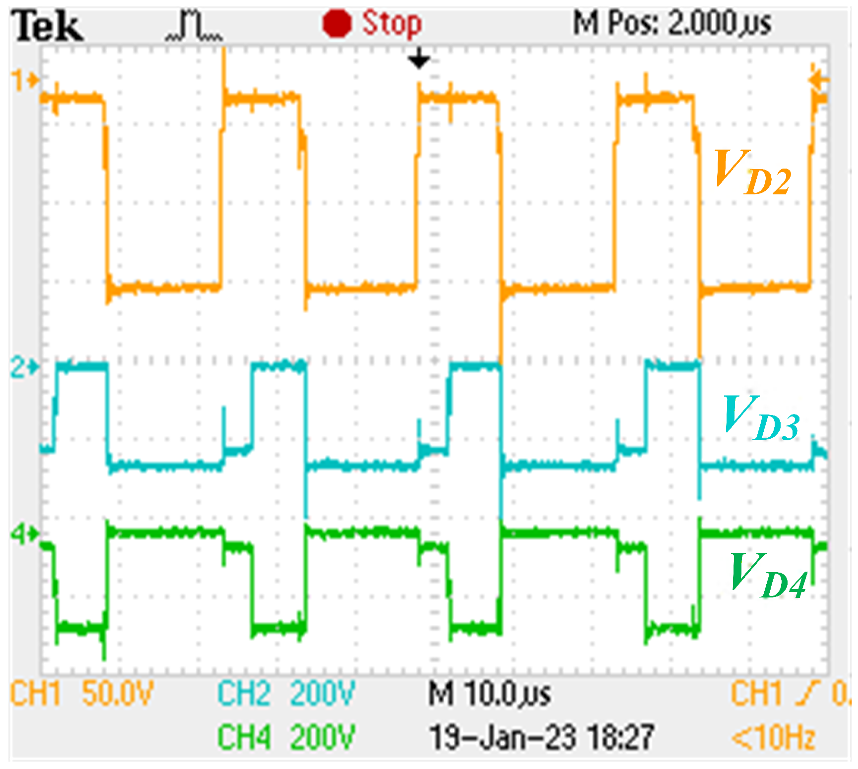
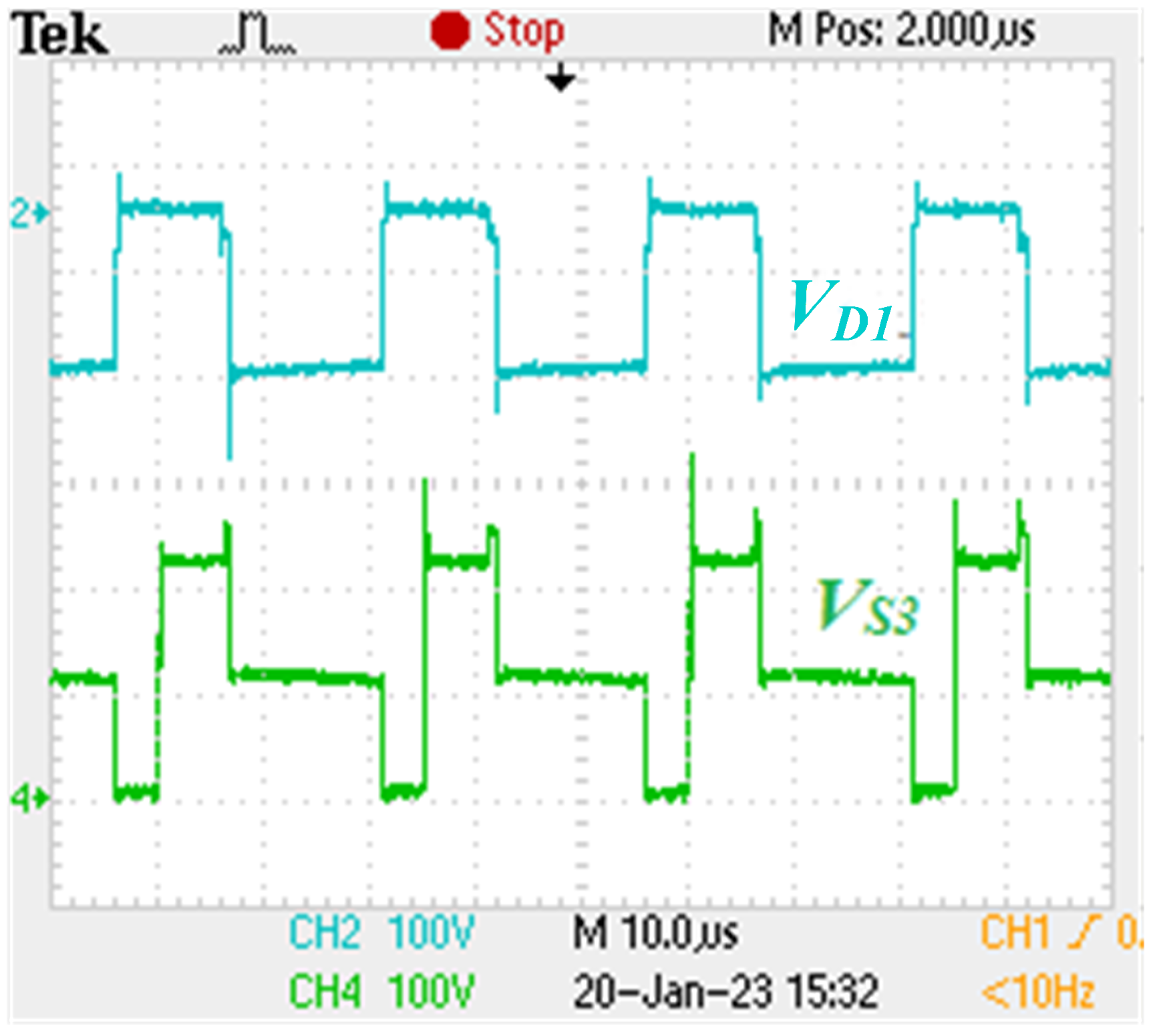
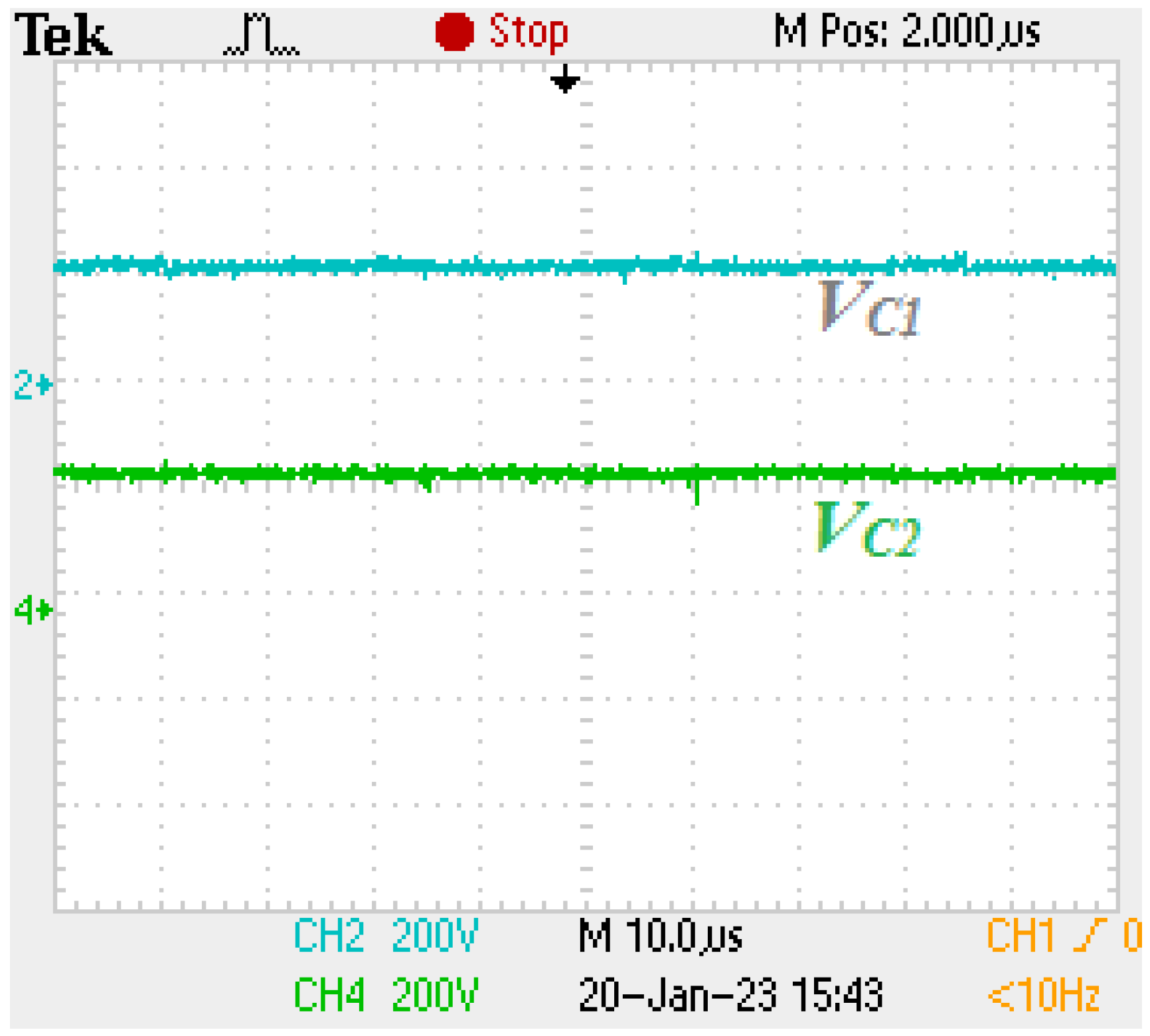
The input–output parameters for converter V i n , I i n and V 0 are captured with values 40 V, 10 A, 394 V, respectively, as shown in Figure 17. The duty cycle kept at D 1 = 0.5 and D 2 = 0.25 respectively and the value of load resistance is R 0 = 400   Ω . The inductors current profile with an average value I L 1 = 7.9 A and I L 2 = 3.95 A presented in Figure 18. The maximum value of voltage of switch S 1 = 120 V and switch S 2 = 150 V shown in Figure 19. The peak value of voltage across diode D 2 = 240 V, D 3 = 280 V and D 4 = 130 V shown in Figure 20. The voltage stress across output diode D 1 = 180 V and auxiliary switch S 3 = 230 V reported in Figure 21. The voltage across capacitor C 1 and C 2 are 230 V, 250 V, respectively, shown in Figure 22.
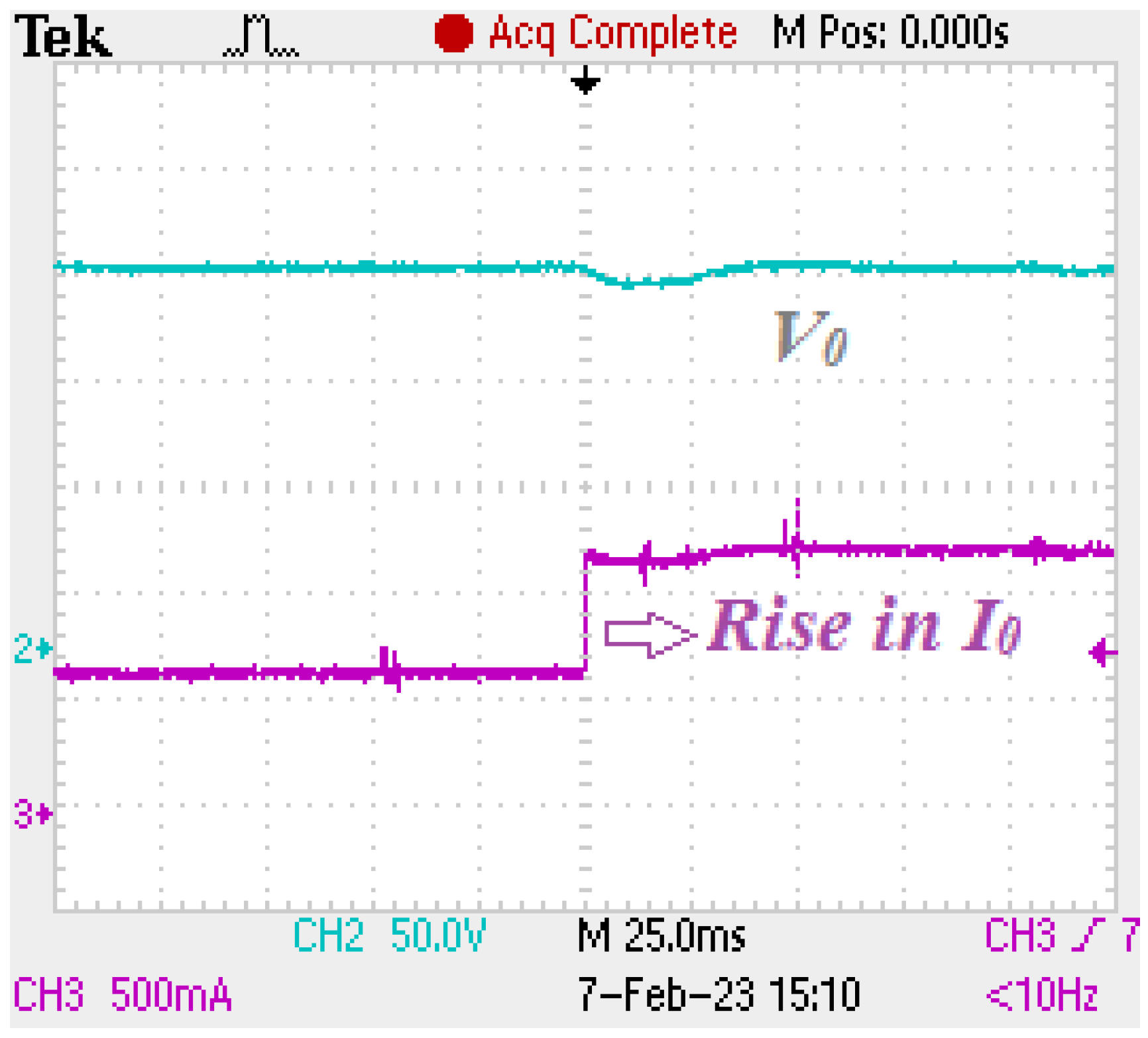
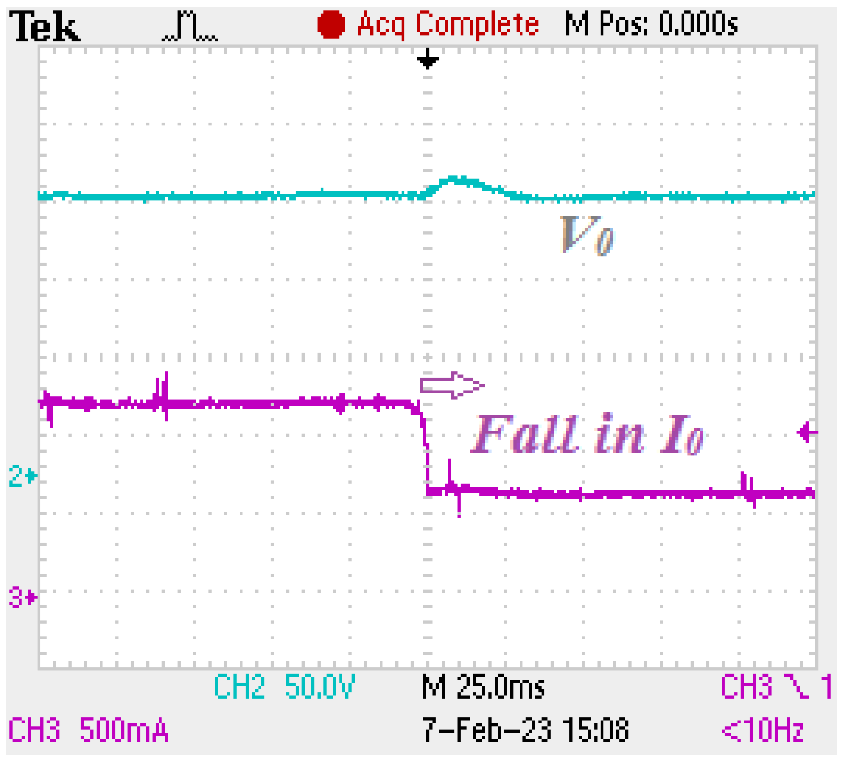
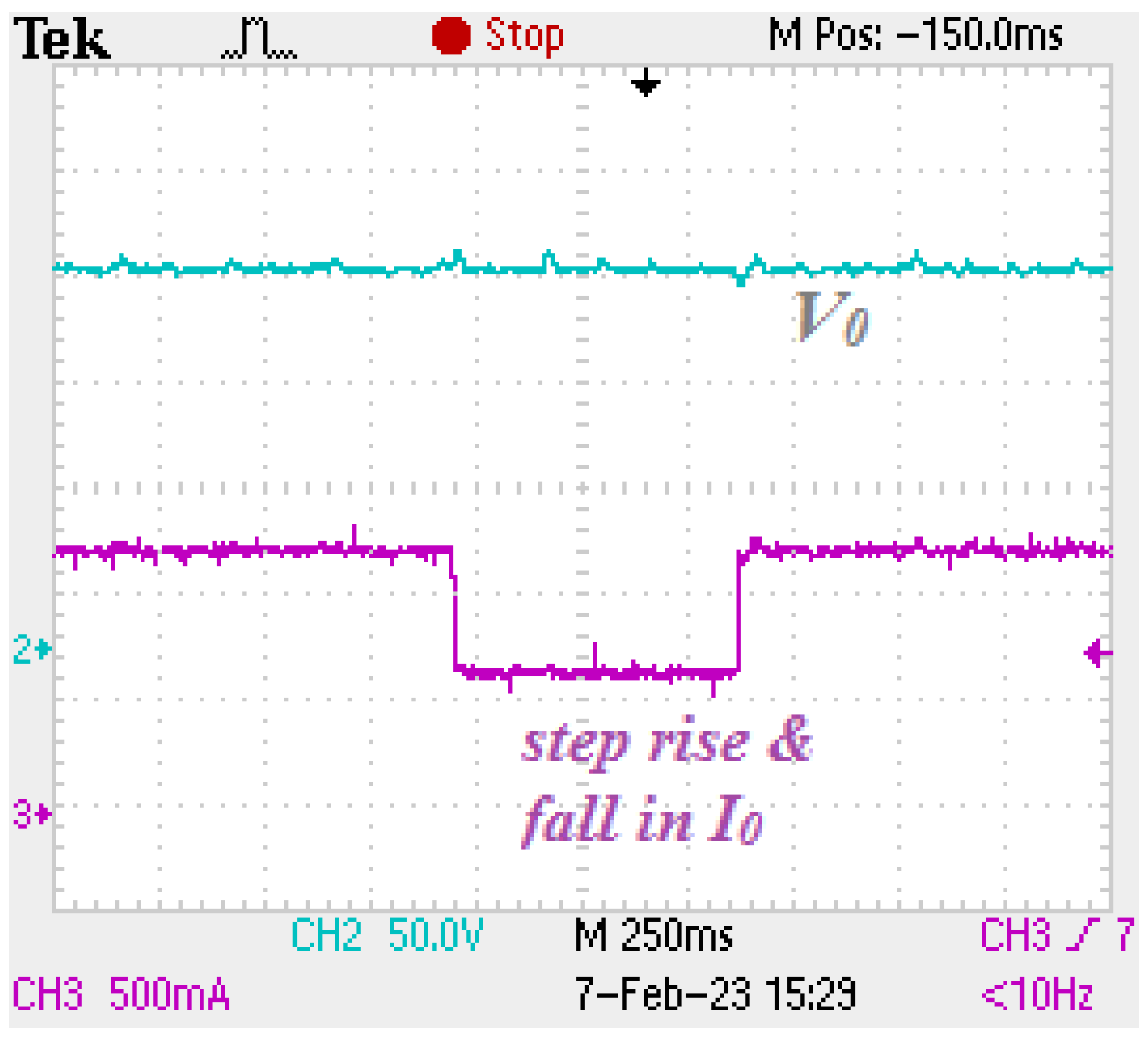
Furthermore, the proposed converter is tested under closed loop condition. A PI controller is used to regulate the output voltage for the load as well input voltage variation. In both, two subcases of step rise and fall in the load current are experimentally verified and the results are captured in Figure 23 and Figure 24, respectively, and the output voltage is maintained as a constant. The steps rise as well as fall in I 0 and both variations are captured in single window of oscilloscope as shown in Figure 25.
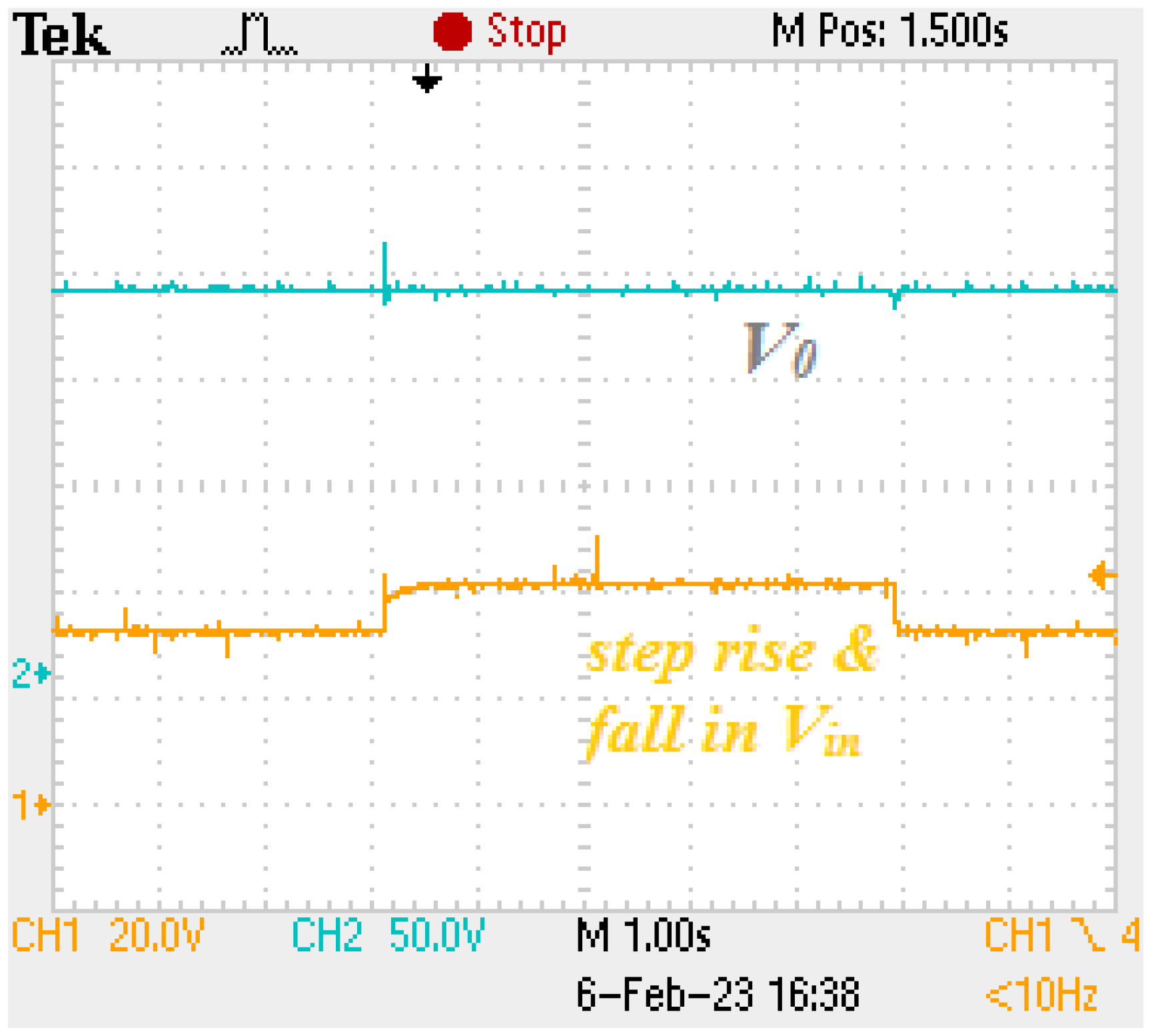
Similarly, variations in supply V i n are captured in Figure 26 and show that the output voltage is maintained as a constant irrespective of load and input supply variation.

5.1. Energy-Based Analysis of Volume of Inductor and Capacitor and Utilization Factor of Switches and Diodes

The size of passive components, like inductors and capacitors, is crucial because it influences the overall size, efficiency, and cost of power converter systems. The size and volume of these components are mostly defined by their energy-storage capacity, which depends on their voltage, current, and permissible ripple. Hence, the volume of the inductor E L is given by
E L = D 1 V i f s Δ i L 1 I L 1 + D 1 V i f s Δ i L 2 I L 2
The capacitor’s volume E C , as determined by
E C = I o V C 1 f s Δ V C 1 + I o V C 2 f s Δ V C 2 + I o D 1 V C o f s Δ V C o
Utilizing Equations (26) and (27), the volume of the inductors and capacitors for the various converters is calculated and presented in Table 4. With the same design limits for all these converters, with an inductor current ripple δ I L of 0.25 % and a capacitor voltage ripple δ V C of 2 %, the size of these converters is evaluated for V i = 40 V, f s = 40 kHz, and R L = 400 Ω . The proposed converter exhibits reduced inductor and capacitor volumes in comparison to [29,30,34,35].
In the cost assessment of the power converter, the cost of the power switches and diodes constitutes a substantial part of the converter cost. Consequently, when comparing costs, the switch utilization factor and the diode utilization factor are considered, and these are illustrated in Equations (28) and (29), respectively. These factors are critical in determining the overall efficiency and performance of the converter, as they directly influence both the initial investment and the long-term operational expenses.
U S = V o I o n = 1 2 V S n I S n , r m s
and
U D = V o I o n = 1 4 V D n I D n , r m s
where V S n , I S n , r m s , V D n , and I D n , r m s are switch voltage stress, switch rms current, diode voltage stress, and diode rms current, respectively. The utilization factor for switches and diodes is calculated for the converters [29,30,34,35] and compared with the proposed converter. The cost of the proposed converter is least among all the converters compared.

5.2. Power Loss Analysis and Efficieny

For power loss calculation parasitic effect of each component is considered: Inductors resistance r L 1 = r L 2 = 0.08   Ω , capacitor resistance r C 1 = r C 2 = 0.15   Ω and r C 0 = 0.3   Ω , MOSFET on state resistance r d s o n = 0.015   Ω , diode drop V f = 0.58   V, diode resistance r d = 0.003   Ω and switching frequency f s w = 40 kHz.
The inductor losses ( P L ) contributed to conduction loss ( P L , c o n d ) and core loss ( P L , c o r e ) given by
P L , c o n d = I L 1 , r m s 2 r L 1 + I L 2 , r m s 2 r L 2
P L , c o r e = 2 [ 71.92 B 1.92 f s 1.47 V e ]
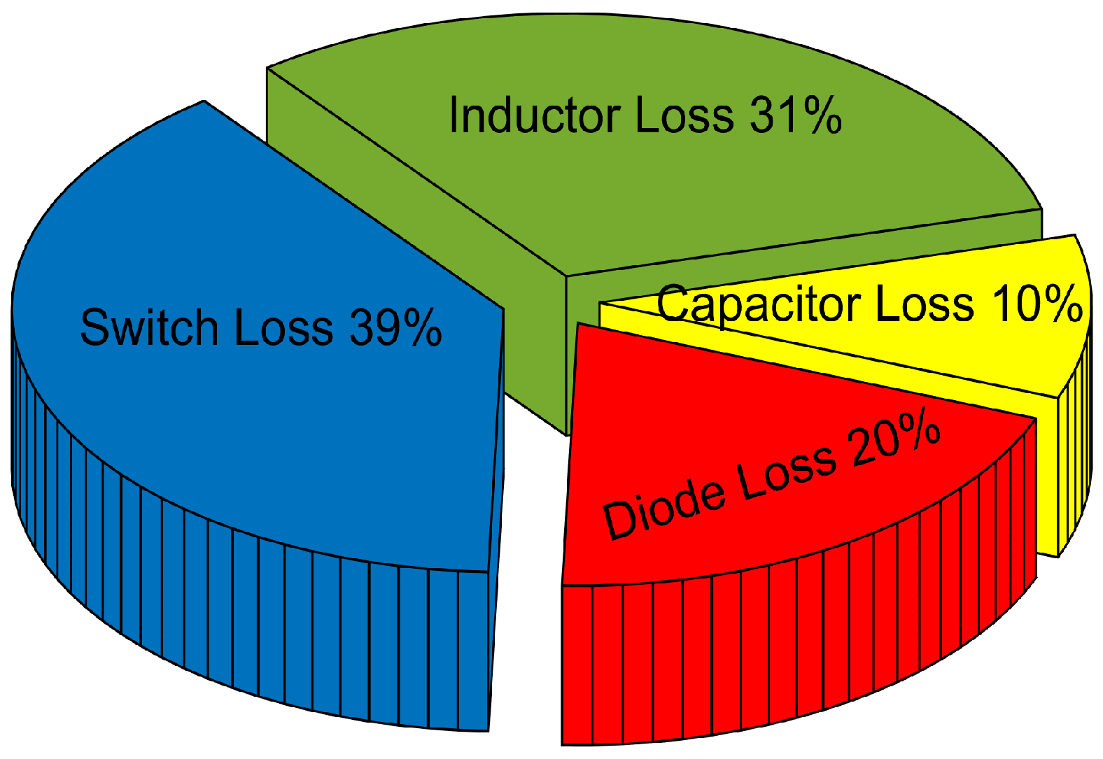
where I L 1 , r m s 2 , I L 1 , r m s 2 are the R M S currents flowing through the inductor L 1 , L 2 , respectively. The losses are contributed by inductor P L = 7.4 W, in which conduction loss is 6.4 W magnetic core loss P L C o r e = 1 W. The losses in the capacitors consist mainly conduction loss, which is expressed as
P C = n = 1 2 I c n , r m s 2 R c n + I c o , r m s 2 . r c o
where, R c n and r c o are the equivalent resistance of the capacitors, and total capacitor loss is P C = 2.7 W.
The Losses in the switches are classified into switching loss ( P S 1 ) and Conduction Loss ( P S 2 ) given by
P S 1 = n = 1 3 t r k + t f k 2 V S n I S ( n , p ) f s
P S 2 = n = 1 3 I s n , r m s R d s n 2
where I S ( n , p ) , I s n , r m s 2 , V S n , R d s n , C S n , t r k , and t f k are the rms current, Peak Current, maximum voltage stress across, turn on resistance, output capacitance, rise time and fall time of the nth switch, respectively. At Nominal operating point I S ( 1 , p ) and I S ( 2 , p ) are 10 A and 8 A, respectively, and reverse voltage stress are V S 1 and V S 2 are 120 V and 240 V, respectively. Therefore, switching losses and conduction losses in the switches are 9.328 W and 1.17 W, respectively. The losses with the diode are also classified into conduction and diode reverse recovery loss, which is expressed as
P D 1 = n = 1 4 I D n , a V F n
P D 2 = n = 1 4 Q r d n V D n f s
where I D n , a , V F n , V D n , and Q r d n are the average diode current, forward diode voltage drop, reverse Voltage stress and reverse recovery charge of the n t h diode, respectively. Thus, the diode’s reverse recovery loss is 2.36 W and its conduction loss is 2.9 W. As a result, the total power loss in the converter is
P L o s s = P L + P L c o r e + P C + P S 1 + P S 2 + P D 1 + P D 2
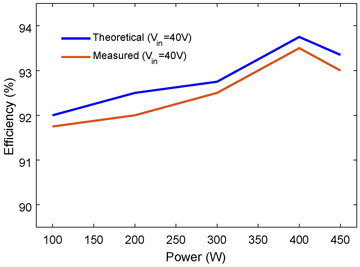
The corresponding efficiency, computed as η = O u t p u t O u t p u t + L o s s e s , is appox. 94 %. Moreover, the efficiency curve variation from 100 W to 450 W along with the comparison of theoretical and measured efficiency is shown in Figure 27 and the percentage loss in the respective converter component for full load (400 W) is depicted in Figure 28.

6. Conclusions

In this manuscript, a dc-dc converter based on a combination of doubly duty cycle ( D 1 and D 2 ) to achieve high gain using SC network is presented for household electrification. By utilizing the additional switch S 3 , flexible high voltage gain is achieved at a low duty cycle of ASL network along with three controller degrees of freedom ( D 1 , D 2 and both D 1 and D 2 ), which can reduce the extra boost converter requirement for the MPPT controller in PV applications. The characteristic waveforms of CCM and DCM are systematically analysed, and the boundary conditions between CCM-DCM are derived and explained in detail. Moreover, design equation, voltage and current stress for semiconductor devices are presented in CCM, and a detailed analysis of power loss, efficiency and comparison with other recent converter topologies is conducted, demonstrating that the proposed converter exerts low stress on semiconductor devices with wide voltage gain. A small signal model is developed and controller is designed to stabilize the plant. The PI controller is used to improve the GM from −51.7 dB to +5.7 dB and PM from −91.4° to +88°, respectively. As the converter shares common ground between its input and output, therefore, zero leakage current presence and reduced EMI effect is ensured. Finally, a laboratory prototype of 400   W output power with duty ratio D 1 = 0.5 , and D = 0.25 to achieve gain equals to 10 times (40/400 V) are included to ascertain the potential of the proposed converter for photovoltaic application. The experimental efficiency also reached to 94% because of absence of oscillation across the switch and lower stress across the components.
The proposed converter has the following limitations: (1) Because of the asymmetric connection of the switch capacitor across all three modes of operation, in mode 1, SC is effectively connected in parallel with L 1 and in series with L 2 ; unequal current sharing occurs in the inductor ( L 1 ) 7.5 A and the inductor ( L 2 ) 3.95 A, which increases the conduction loss and thermal stress. (2) The capacitor is experiencing high ripple current stress, so a high-power rating (KW) and the need for a low effective series resistance (ESR) and high ripple current capability capacitor are required. These limitations can be addressed in future work.

Author Contributions

Conceptualization, Writing-original draft, S.K. (Sahendara Kumar); Validation, S.K. (Sajid Kamal), writing—review and editing, Supervision, A.K.; Funding acquisition, X.P. All authors have read and agreed to the published version of the manuscript.

Funding

This project is funded under the grant no. SPARC/2025-2026/P4262 received from The Scheme for Promotion of Academic and Research Collaboration, India.

Data Availability Statement

The original contributions presented in the study are included in the article, further inquiries can be directed to the corresponding author.

Conflicts of Interest

The authors declare no conflicts of interest.

References

  1. Williamson, S.S.; Rathore, A.K.; Musavi, F. Industrial electronics for electric transportation: Current state-of-the-art and future challenges. IEEE Trans. Ind. Electron. 2015, 62, 3021–3032. [Google Scholar] [CrossRef]
  2. Dhananjaya, M.; Sathik, J.; Mekhilef, S.; Alghaythi, M.L. New Single-Input Dual-Output Converter for DC Nanogrid Application. IEEE Trans. Consum. Electron. 2025, 71, 3294–3303. [Google Scholar] [CrossRef]
  3. Reza, M.; Kumar, A.; Wang, Y.; Raghuram, M.; Naresh, P.; Singh, S.K.; Xiong, X.P.X. High gain quasi switched boost inverter with optimal performance parameters. IEEE Trans. Transp. Electrif. 2020, 6, 554–567. [Google Scholar] [CrossRef]
  4. Vijayan, M.; Udumula, R.R.; Mahto, T. A Novel High Gain Tertiary Port Boost Converter for Hybrid Energy System Integration. IEEE Trans. Consum. Electron. 2024, 71, 643–654. [Google Scholar] [CrossRef]
  5. Varesi, K.; Hassanpour, H.; Saeidabadi, S. Novel high step-up DC–DC converter with increased voltage gain per devices and continuous input current suitable for DC microgrid applications. Int. J. Circuit Theory Appl. 2020, 48, 1820–1837. [Google Scholar] [CrossRef]
  6. Chub, A.; Vinnikov, D.; Blaabjerg, F.; Peng, F.Z. A review of galvanically isolated impedance-source dc–dc converters. IEEE Trans. Power Electron. 2016, 31, 2808–2828. [Google Scholar] [CrossRef]
  7. Pan, X.; Li, H.; Liu, Y.; Zhao, T.; Ju, C.; Rathore, A.K. An overview and comprehensive comparative evaluation of current-fed-isolated-bidirectional DC/DC converter. IEEE Trans. Power Electron. 2019, 35, 2737–2763. [Google Scholar] [CrossRef]
  8. Islam, S.; Marzang, V.; Iqbal, A.; Mehrjerdi, H.; Ahmed, H.F.; Samiullah, M.; Bakhsh, F.I. An Extendable High Step-up Quadratic Boost Topology Having low Voltage Stress on MOSFETs. IEEE Trans. Consum. Electron. 2025, 71, 7947–7958. [Google Scholar] [CrossRef]
  9. Zhu, M.; Luo, F. Series sepic implementing voltage-lift technique for DC–DC power conversion. IET Power Electron. 2008, 1, 109–121. [Google Scholar] [CrossRef]
  10. Lei, H.; Hao, R.; You, X.; Li, F.; Zhou, M. Nonisolated High Step-Up Soft-Switching DC-DC Converter Integrating Dickson Switched-Capacitor Techniques. In Proceedings of the 2018 IEEE Energy Conversion Congress and Exposition (ECCE), Portland, OR, USA, 23–27 September 2018. [Google Scholar]
  11. Liu, H.; Hu, H.; Wu, H.; Xing, Y.; Batarseh, I. Overview of high-step-up coupled-inductor boost converters. IEEE J. Emerg. Sel. Top. Power Electron. 2016, 4, 689–704. [Google Scholar] [CrossRef]
  12. Kumar, A.; Xiong, X.; Pan, X.; Reza, M.; Beig, A.R.; Jaafari, K.A. A wide voltage gain bidirectional DC–DC converter based on quasi Z-source and switched capacitor network. IEEE Trans. Circuits Syst. II Express Briefs 2020, 68, 1353–1357. [Google Scholar] [CrossRef]
  13. Elsayad, N.; Moradisizkoohi, H.; Mohammed, O.A. A new single-switch structure of a DC–DC converter with wide conversion ratio for fuel cell vehicles: Analysis and development. IEEE J. Emerg. Sel. Top. Power Electron. 2019, 8, 2785–2800. [Google Scholar] [CrossRef]
  14. Singh, A.; Siva, V.; Kumar, A.; Singh, S.K. Analysis and Design of Switched LC Converter with reduced Voltage stress for Photovoltaic applications. IEEE Trans. Ind. Appl. 2023, 59, 6468–6479. [Google Scholar] [CrossRef]
  15. Varesi, K.; Ghorbani, M. A generalized common-ground single-switch continuous input-current boost converter favourable for DC microgrids. Int. J. Circuit Theory Appl. 2020, 48, 1658–1675. [Google Scholar] [CrossRef]
  16. Lee, S.S.; Chu, B.; Lim, C.S.; Lee, K.-B. Two-inductor non-isolated DC-DC converter with high step-up voltage gain. J. Power Electron. 2019, 19, 1069–1073. [Google Scholar]
  17. Rosas-Caro, J.C.; Ramirez, J.M.; Peng, F.Z.; Valderrabano, A. A DC-DC multilevel boost converter. IET Power Electron. 2010, 3, 129–137. [Google Scholar] [CrossRef]
  18. Hu, X.; Gong, C. A High Gain Input-Parallel Output-Series DC/DC Converter with Dual Coupled Inductors. IEEE Trans. Power Electron. 2015, 30, 1306–1317. [Google Scholar] [CrossRef]
  19. Prabhala, V.A.K.; Fajri, P.; Gouribhatla, V.S.P.; Baddipadiga, B.P.; Ferdowsi, M. A DC–DC Converter With High Voltage Gain and Two Input Boost Stages. IEEE Trans. Power Electron. 2016, 31, 4206–4215. [Google Scholar] [CrossRef]
  20. Baddipadiga, B.P.; Ferdowsi, M. A high-voltage-gain dc-dc converter based on modified dickson charge pump voltage multiplier. IEEE Trans. Power Electron. 2017, 32, 7707–7715. [Google Scholar] [CrossRef]
  21. Yang, L.-S.; Liang, T.-J.; Chen, J.-F. Transformerless DC–DC converters with high step-up voltage gain. IEEE Trans. Ind. Electron. 2009, 56, 3144–3152. [Google Scholar] [CrossRef]
  22. Tang, Y.; Wang, T.; He, Y. A switched-capacitor-based active-network converter with high voltage gain. IEEE Trans. Power Electron. 2013, 29, 2959–2968. [Google Scholar] [CrossRef]
  23. Krishna, B.; Karthikeyan, V. Active switched-inductor network step-up DC–DC converter with wide range of voltage-gain at the lower range of duty cycles. IEEE J. Emerg. Sel. Top. Ind. Electron. 2021, 2, 431–441. [Google Scholar] [CrossRef]
  24. Gu, Y.; Chen, Y.; Zhang, B.; Qiu, D.; Xie, F. High step-up DC–DC converter with active switched LC-network for photovoltaic systems. IEEE Trans. Energy Convers. 2018, 34, 321–329. [Google Scholar] [CrossRef]
  25. Tang, Y.; Wang, T. Study of an improved dual-switch converter with passive lossless clamping. IEEE Trans. Ind. Electron. 2014, 62, 972–981. [Google Scholar] [CrossRef]
  26. Mohammed, M.R.; Al-Sumaiti, A.S.; Beig, A.R.; Hosani, K.A.; Wang, C. A common grounded voltage quadrupler ASL/PSC hybrid converter with reduced voltage stress. IEEE Trans. Ind. Electron. 2023, 71, 4773–4784. [Google Scholar] [CrossRef]
  27. Li, H.; Chen, D. A novel high step-up non-isolated quasi-Z-source DC-DC converter with active switched inductor and switched capacitor. IEEE J. Emerg. Sel. Top. Power Electron. 2023, 11, 5062–5077. [Google Scholar] [CrossRef]
  28. Elsayad, N.; Moradisizkoohi, H.; Mohammed, O. A new SEPIC-based step-up DC-DC converter with wide conversion ratio for fuel cell vehicles: Analysis and design. IEEE Trans. Ind. Electron. 2020, 68, 6390–6400. [Google Scholar] [CrossRef]
  29. Lakshmi, M.; Hemamalini, S. Nonisolated High Gain DC–DC Converter for DC Microgrids. IEEE Trans. Ind. Electron. 2018, 65, 1205–1212. [Google Scholar] [CrossRef]
  30. Bhaskar, M.S.; Alammari, R.; Meraj, M.; Padmanaban, S.; Iqbal, A. A New Triple-Switch-Triple-Mode High Step-Up Converter With Wide Range of Duty Cycle for DC Microgrid Applications. IEEE Trans. Ind. Appl. 2019, 55, 7425–7441. [Google Scholar] [CrossRef]
  31. Maroti, P.K.; Al-Ammari, R.; Bhaskar, M.S.; Meraj, M.; Iqbal, A.; Sanjeevikumar, P.; Rahman, S. A Novel High Gain Three-State Switching Hybrid Boost Converter for DC Microgrid Applications. IET Power Electron. 2019, 12, 2741–2750. [Google Scholar] [CrossRef]
  32. Bhaskar, M.S.; Meraj, M.; Iqbal, A.; Padmanaban, S.; Maroti, P.K.; Alammari, R. High Gain Transformer-Less Double-Duty-Triple-Mode DC/DC Converter for DC Microgrid. IEEE Access 2019, 7, 36353–36370. [Google Scholar] [CrossRef]
  33. Maroti, P.K.; Padmanaban, S.; Bhaskar, M.S.; Meraj, M.; Iqbal, A.; Al-Ammari, R. High gain three-state switching hybrid boost converter for DC microgrid applications. IET Power Electron. 2019, 12, 3656–3667. [Google Scholar] [CrossRef]
  34. Marzang, V.; Hosseini, S.H.; Rostami, N.; Alavi, P.; Mohseni, P.; Hashemzadeh, S.M. A High Step-Up Nonisolated DC–DC Converter With Flexible Voltage Gain. IEEE Trans. Power Electron. 2020, 35, 10489–10500. [Google Scholar] [CrossRef]
  35. Iqbal, A.; Gore, S.; Maroti, P.K.; Islam, S.; Meraj, M.; Marzband, M. A new triswitching double duty high voltage gain boost converter for DC nanogrid application. IEEE Trans. Ind. Appl. 2023, 59, 6242–6250. [Google Scholar] [CrossRef]
  36. Samiullah, M.; Bhaskar, M.S.; Meraj, M.; Iqbal, A.; Ashraf, I.; Komurcugil, H. High gain switched-inductor-double-leg converter with wide duty range for DC microgrid. IEEE Trans. Ind. Electron. 2020, 68, 9561–9573. [Google Scholar] [CrossRef]
  37. Cheng, T.; Dah-ChuanLu, D.; Siwakoti, Y.P. Electro-Thermal Average Modeling of a Boost Converter Considering Device Self-heating. In Proceedings of the 2020 IEEE Applied Power Electronics Conference and Exposition (APEC), New Orleans, LA, USA, 15–19 March 2020; pp. 2854–2859. [Google Scholar] [CrossRef]
  38. Górecki, K.; Górecki, P. Electrothermal Averaged Model of a Half-Bridge DC–DC Converter Containing a Power Module. Electronics 2024, 13, 3662. [Google Scholar] [CrossRef]
  39. Erickson, R.W.; Maksimovic, D. Fundamentals of Power Electronics; Springer Science & Business Media: Berlin/Heidelberg, Germany, 2007. [Google Scholar]
  40. Tang, Y.; Wang, T.; He, Y.; Fu, D. Study of a high step-up voltage gain DC/DC converter with passive lossless clamp circuit. In IECON 2013-39th Annual Conference of the IEEE Industrial Electronics Society; IEEE: New York, NY, USA, 2013; pp. 1308–1313. [Google Scholar]
  41. Salvador, M.A.; de Andrade, J.M.; Lazzarin, T.B.; Coelho, R.F. Nonisolated high-step-up DC–DC converter derived from switched-inductors and switched-capacitors. IEEE Trans. Ind. Electron. 2019, 67, 8506–8516. [Google Scholar] [CrossRef]
  42. Salvador, M.A.; Lazzarin, T.B.; Coelho, R.F. High step-up DC–DC converter with active switched-inductor and passive switched-capacitor networks. IEEE Trans. Ind. Electron. 2017, 65, 5644–5654. [Google Scholar] [CrossRef]
Figure 1. DC microgrid showing the use of solar energy.
Energies 19 02773 g001
Figure 2. Proposed high gain dc-dc converter.
Energies 19 02773 g002
Figure 3. Waveform of CCM.
Energies 19 02773 g003
Figure 4. Mode-1 Equivalent circuit diagram.
Energies 19 02773 g004
Figure 5. Mode-2 Equivalent circuit diagram.
Energies 19 02773 g005
Figure 6. Mode-3 Equivalent circuit diagram.
Energies 19 02773 g006
Figure 7. Voltage gain of converter in CCM.
Energies 19 02773 g007
Figure 8. Waveform of DCM.
Energies 19 02773 g008
Figure 9. Proposed converter boundary condition.
Energies 19 02773 g009
Figure 10. Proposed Converter with Parasitic parameters.
Energies 19 02773 g010
Figure 11. Comparison of voltage gain with various converters [29,30,32,33,34,35,41,42] for D 2 = 0.25 .
Energies 19 02773 g011
Figure 12. Comparison of normalized switch stress across S 3 with various converters [29,30,33,34,35].
Energies 19 02773 g012
Figure 13. Voltage and current stress of switch.
Energies 19 02773 g013
Figure 14. Control structure of proposed TSTM.
Energies 19 02773 g014
Figure 15. Bode plot of converter without and with controller.
Energies 19 02773 g015
Figure 16. Photograph of proposed converter.
Energies 19 02773 g016
Figure 17. Input–output voltage and current waveform.
Energies 19 02773 g017
Figure 18. Zoomed Inductor current profile.
Energies 19 02773 g018
Figure 19. Voltage stress of main switch S 1 and S 2 .
Energies 19 02773 g019
Figure 20. Voltage stress of intermediate diode D 2 , D 3 and D 4 .
Energies 19 02773 g020
Figure 21. Voltage stress of output diode D 1 and auxiliary switch S 3 .
Energies 19 02773 g021
Figure 22. Average value of intermediate capacitor voltage.
Energies 19 02773 g022
Figure 23. Dynamic performance under step rise in I 0 .
Energies 19 02773 g023
Figure 24. Dynamic performance under step fall in I 0 .
Energies 19 02773 g024
Figure 25. Dynamic behaviour under both rise and fall in I 0 .
Energies 19 02773 g025
Figure 26. Dynamic behaviour both rise and fall in V i n .
Energies 19 02773 g026
Figure 27. Comparison of theoretical and measured efficiency.
Energies 19 02773 g027
Figure 28. Power loss distribution at 400 W.
Energies 19 02773 g028
Table 1. Current stress on capacitor and diodes.
ElementMode-1Mode-2Mode-3
i C 1 I 0 D 1 0 I 0 ( 1 D 1 D 2 )
i C 2 I 0 D 1 0 I 0 ( 1 D 1 D 2 )
i C 0 I 0 I 0 I 0 ( D 1 + D 2 ) ( 1 D 1 D 2 )
i D 1 0 2 I 0 ( 1 D 1 D 2 ) 0
i D 2 00 I 0 ( 1 D 1 D 2 )
i D 3 I 0 D 1 00
i D 4 00 I 0 ( 1 D 1 D 2 )
i S 1 ( 1 + D 1 D 2 ) I 0 ( 1 D 1 D 2 ) D 1 00
i S 2 ( 1 D 2 ) I 0 ( 1 D 1 D 2 ) D 1 I 0 ( 1 D 1 D 2 ) 0
i S 3 0 2 I 0 ( 1 D 1 D 2 ) 0
Table 2. Voltage stress across diodes and switches.
DevicesMode-1Mode-2Mode-3
V D 1 V i n 0 ( 1 + D 1 ) V i n ( 1 D 1 D 2 )
V D 2 ( 2 D 2 ) V i n ( 1 D 1 D 2 ) ( 1 + D 1 ) V i n ( 1 D 1 D 2 ) 0
V D 3 0 V i n ( 2 D 2 ) V i n ( 1 D 1 D 2 )
V D 4 ( 1 D 2 ) V i n ( 1 D 1 D 2 ) D 1 V i n ( 1 D 1 D 2 ) 0
V S 1 0 V i n ( 1 D 2 ) V i n ( 1 D 1 D 2 )
V S 2 00 V i n ( 1 D 1 D 2 )
V S 3 V i n 0 ( 1 + D 1 ) V i n ( 1 D 1 D 2 )
Table 3. Comparison of proposed topology with existing topologies.
TopologyLCSDTCGainMaximum SwitchMaximum SwitchMaximum DiodeEfficiencyInputCommon
Voltage StressCurrent StressVoltage stress CurrentGround
Converter [42]332210 1 + 3 D 1 D V S 1 = V S 2 = V 0 1 + 3 D I S 1 = I S 2 = 2 ( 1 + D ) 1 D I 0 V D 1 = V D 1 = 2 V 0 1 + 3 D 95.9%continuousNO
Converter [41]232310 3 + D 1 D V S 1 = V S 2 = V 0 3 + D I S 1 = I S 2 = 4 I 0 1 D V D 1 = V D 2 = 2 V 0 3 + D 96%continuousNO
V D 0 = 2 V 0 3 + D
Converter [29]21328 1 + D 1 1 D 1 D 2 V S 1 = V S 2 = ( 2 D 2 ) V 0 2 ( 1 + D 1 ) I S 1 = I S 2 = I 0 1 D 1 D 2 V D 1 = ( 1 D 1 D 2 ) V 0 1 + D 1 95%continuousNO
V S 3 = V 0 I S 3 = I 0 1 D 1 D 2 V D 2 = 2 D 2 1 + D 1 V 0
Converter [32]223310 2 D 2 1 D 1 D 2 V S 1 = ( 1 D 1 D 2 ) V 0 2 ( 2 D 2 ) I S 1 = I S 2 = 2 D 2 1 D 1 D 2 I 0 V D 1 = V 0 2 96%continuousNO
V S 2 = ( 1 D 1 D 2 ) V 0 2 ( 2 D 2 ) I S 3 = 2 D 2 1 D 1 D 2 V D 2 = ( 1 + D 1 ) V 0 1 D 1 D 2
V S 3 = 1 + D 1 1 D 1 D 2 V 0
Converter [35]223310 2 1 D 1 D 2 V S 1 = V S 2 = V 0 2 I S 1 = I S 3 = I 0 1 D 1 D 2 V D 1 = V D 2 = V 0 2 95%continuousNO
V S 3 = V 0 2 I S 2 = I 0 D 1 ( 1 D 1 D 2 ) V D 0 = V 0
Converter [30]232210 3 D 1 2 D 2 1 D 1 D 2 V S 1 = ( 2 D 2 ) 2 ( 3 D 1 2 D 2 ) V 0 I S 1 = 3 D 1 2 D 2 1 D 1 D 2 I 0 V D 1 = ( 2 D 2 ) 2 ( 3 D 1 2 D 2 ) V 0 93.2%continuousNO
V S 2 = ( 2 D 2 ) 2 ( 3 D 1 2 D 2 ) V 0 I S 2 = 3 D 1 2 D 2 1 D 1 D 2 I 0 V D 2 = ( 2 D 2 ) 2 ( 3 D 1 2 D 2 ) V 0
V S 3 = ( 1 + D 1 ) 3 D 1 2 D 2 V 0 I S 3 = 3 D 1 2 D 2 1 D 1 D 2 I 0 V D 0 = ( 2 D 2 ) 3 D 1 2 D 2 V 0
Converter [33]233412 3 D 1 D 2 1 D 1 D 2 V S X = V 0 3 D 1 D 2 I S X = 1 + 2 D 1 ( 1 D 1 D 2 ) D 1 I 0 V D X = V 0 3 D 1 D 2 95.1%continuousNO
V S Y = V 0 3 D 1 D 2 I S Y = 1 D 2 ( 1 D 1 D 2 ) D 1 I 0 V D Y = V 0 3 D 1 D 2
V S Z = V 0 I S Z = 3 D 1 D 2 2 ( 1 D 1 D 2 ) I 0 V D Z = V 0
Converter [34]233412 3 + D 1 D 2 1 D 1 D 2 V S 1 = ( 2 D 2 ) V 0 2 ( 3 + D 1 D 2 ) I S 1 = 1 + D 1 D 2 ( 1 D 1 D 2 ) D 1 I 0 V D 1 = ( 2 D 2 ) V 0 ( 3 + D 1 D 2 ) 96.8%continuousNO
V S 2 = ( 2 D 2 ) V 0 2 ( 3 + D 1 D 2 ) I S 2 = 1 + D 1 D 2 ( 1 D 1 D 2 ) D 1 I 0 V D 2 = ( 2 D 2 ) V 0 ( 3 + D 1 D 2 )
V S 3 = 1 + D 1 ( 3 + D 1 D 2 ) V 0 I S 3 = 2 I 0 ( 1 D 1 D 2 ) D 1 I 0 V D 0 = 2 D 2 ( 3 + D 1 D 2 ) V 0
Proposed converter233412 3 2 D 2 1 D 1 D 2 V S 1 = 1 D 2 3 2 D 2 V 0 I S 1 = 1 + D 1 D 2 1 D 1 D 2 I 0 V D 1 = 1 D 1 D 2 3 2 D 2 V 0 97.1%continuousYES
V S 2 = V 0 3 2 D 2 I S 2 = 1 D 2 1 D 1 D 2 I 0 V D 2 , D 3 = 2 D 2 3 2 D 2 V 0
V S 3 = 1 + D 1 3 2 D 2 V 0 I 31 = 2 I 0 1 D 1 D 2 V D 4 = 1 D 2 3 2 D 2 V 0
Note1: In this table L = number of inductor, C = number of capacitor, S = number of switches, D = number of diodes, TC total count, D = Duty cycle of converter. Note2: Efficiency number calculated for 400 W power rating and Switching frequency f s = 40 kHz.
Table 4. Specifications of the components of different converters.
Converter [29]Converter [30]Converter [35]Converter [34]Proposed Converter
Input Switch S 1 , S 2 : IRFB4137PBF, 300 V, 40 A Price: 2 × $3.77 S 1 , S 2 : IRFB4332 PBF, 250 V, 60 A Price: 2 × $3 S x , S y : RFB4332 PBF, 250 V, 60 A Price: 2 × $3 S 1 , S 2 : IRFP260 MPBF, 200 V, 50 A Price: 2 × $3 S 1 , S 2 : IRFB4137PBF, 300 V, 40 A Price: 2 × $3.77
Output switch S 3 : 26NM60N 600 V, 20 A Price: 1 × $4 S 3 : 26NM60N 600 V, 20 A Price: 1 × $4 S z : RFB4332 PBF, 250 V, 60 A Price: 1 × $3 S 3 : IRFB4137PBF, 300 V, 40 A Price: 1 × $3 S 3 : 26NM60N 600 V, 20 A Price: 1 × $4
Input Diodes D 1 : C6D10065A, 650 V, V f = 1.27  V Price: 1 × $4.30 D 1 , D 2 , D 3 : MBR40250G, 250 V, V f = 0.86  V Price: 3 × $1.75 D 1 , D 2 : SBR20A300 CTB, 300 V V f = 1.06  V Price: 2 × $2.10 D 1 , D 2 , D 3 : SBR20A300CTB 300 V V f = 1.06  V Price: 3 × $2.10 D 2 , D 3 SBR20A300 CTB, 300 V V f = 1.06  V Price: 2 × $2.10
Output Diode D O : C6D10065A, 650 V, V f = 1.27  V Price: 1 × $4.30 D o : STTH30R04, 400 V, V f = 0.97  V Price: 1 × $3.30 D o : C6D10065A, 650 V, V f = 1.27  V Price: 1 × $4.30 D o SBR20A300 CTB, 300 V V f = 1.06  V Price: 1 × $2.10 D 1 , D o MBR30200CT, 200 V V f = 0.85 Price: 2× $1.12
Inductors L 1 , L 2 : 240 μ H 6.67 A, 60 m Ω PCV-2-274-05 Price: 2 × $8.60 L 1 , L 2 : 220 μ H 10.1 A, 32 m Ω PCV-2-274-10 Price: 2 × $6.92 L 1 , L 2 : 220 μ H 10 A, 32 m Ω PCV-2-274-10 Price: 2 × $6.92 L 1 , L 2 : 230 μ H 6.67 A, 60 m Ω PCV-2-274-05 Price: 2 × $8.60 L 1 , L 2 : 200 μ H 8 A, 48 m Ω PCV-2-184-10L Price: 2 × $6.72
Capacitors C o : 250   μ F REA1650101M450B Al Electrolytic, 450 V Price: $4.25 C 1 , C 2 : 250 μ F UPW1H101MPD1FA Al Electrolytic, 100 V Price: 2 × $1.5 C o : 138 μ F REA1650101M450BAl Electrolytic, 450 V Price: $3.79 C 1 : 562 μ F, Al Electrolytic, 100 V Price: $1.57 C o : 200 μ F 870055975004, Al Electrolytic, 450 V Price: $3.79 C 1 , C 2 : 250 μ F Electrolytic, 200 V Price: 2 × $1.05 C o : 137 μ F Electrolytic, 600 V Price: 1 × $1.57 C 1 , C 2 : 100 μ F EGXF351ELL620M-U30S, Electrolytic, 350 V Price: 2 × $1.05 C O : 50 μ F UTH2W620MND Electrolytic, 450 V Price: 1 × $1.15
Gate-drivers required33333
Input/output voltage40 V/400 V40 V/400 V40 V/400 V40 V/400 V40 V/400 V
Output power400 W400 W400 W400 W400 W
E L 0.0480.0440.0440.0310.024
E C 0.100.0750.110.1050.072
U S 0.1130.0940.1470.1870.258
U D 0.1670.2170.2010.1850.322
Cost$41.59$43.1$36.7$38.27$33.55
Table 5. Specification and parameter of converter.
Specification
Input Voltage V i n 40 V
Output Voltage V 0 394 V
Output Power P 0 400 W
Switching frequency f s w 40 kHz
Parameter
Inductance L 1 420 μ H
Inductance L 2 420 μ H
Capacitance C 1 63 μ F
Capacitance C 2 33 μ F
Capacitance C 0 63 μ F
Table 6. Comparison of calculated and measured values.
ParameterCalculatedMeasured
Input Voltage V i n 40 V40 V
ConverterOutput Voltage V 0 400 V394 V
Output Power P 0 400 W394 W
Max.votage stress ( S 1 ; S 2 ) 120 V; 160 V120 V; 150 V
Converter Max.votage stress ( S 3 ) 240 V230 V
Max.votage stress ( D 1 ; D 2 ) 240 V; 280 V180 V; 240 V
Max.votage stress ( D 3 ; D 4 ) 280 V; 120 V280 V; 130 V
Max.votage stress ( C 1 ; C 2 ) 240 V; 280 V230 V; 250 V
Max.votage stress ( C O ) 400 V394 V
Avg. Inductor current ( i L 1 ; i L 2 )8 A; 4 A7.9 A; 3.95 A
Disclaimer/Publisher’s Note: The statements, opinions and data contained in all publications are solely those of the individual author(s) and contributor(s) and not of MDPI and/or the editor(s). MDPI and/or the editor(s) disclaim responsibility for any injury to people or property resulting from any ideas, methods, instructions or products referred to in the content.