
Digital Control Scheme for Class-D Power Amplifier Driving ICP Load Without Matching Network


Abstract
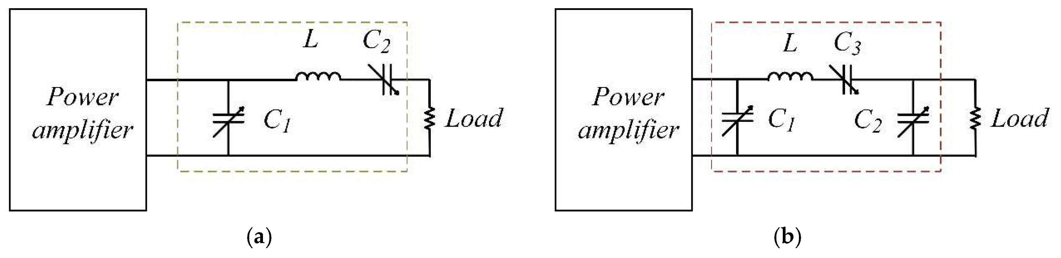
1. Introduction
- (1)
- Proposing a full-digital control scheme for Class-D power amplifiers to directly drive variable loads such as ICP, with a detailed analysis of the impact of PFM resolution on output power accuracy.
- (2)
- A method for high-resolution DPWM/DPFM generation with a simple structure is designed using an FPGA, thereby enhancing the temporal resolution of the drive signal generated.
- (3)
- Proposing a real-time phase measurement method that does not require a VI probe to calculate the phase of the output voltage and current in real-time, with a time accuracy of 53 ps. It can also calculate the output power in real-time, reducing hardware costs. This phase measurement scheme is not only applicable to Class-D power amplifiers but also to half-bridge or full-bridge resonant topologies, with a broad application prospect.
- (4)
- Proposing a dynamic dead-time calculation method to ensure ZVS in Class-D power amplifiers. It can also be used for real-time ZVS state judgment without the need for separate ZVS detection hardware circuits.
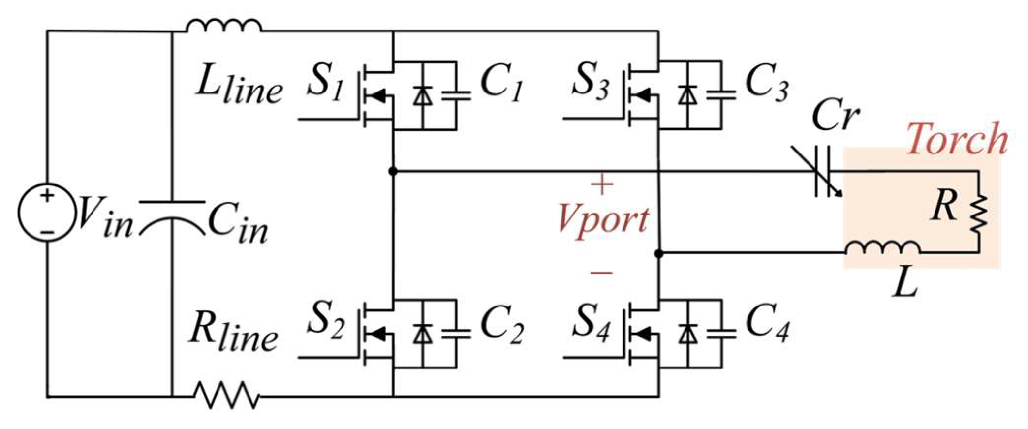
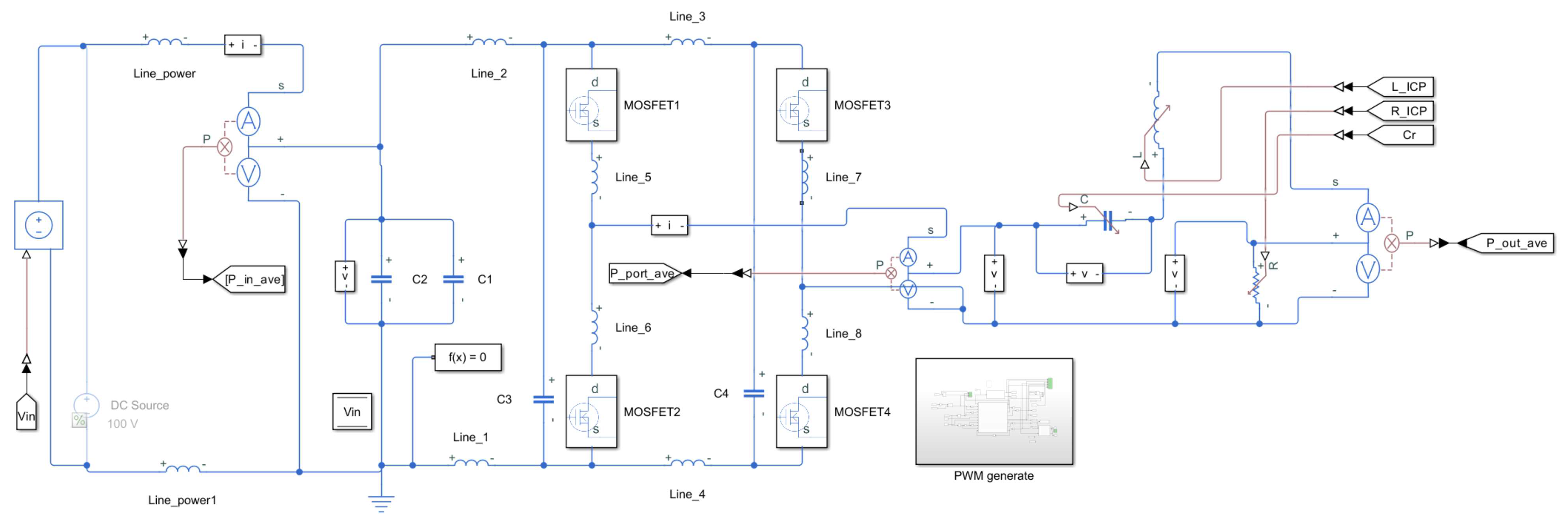
2. Overall Introduction to the Digital Control Scheme
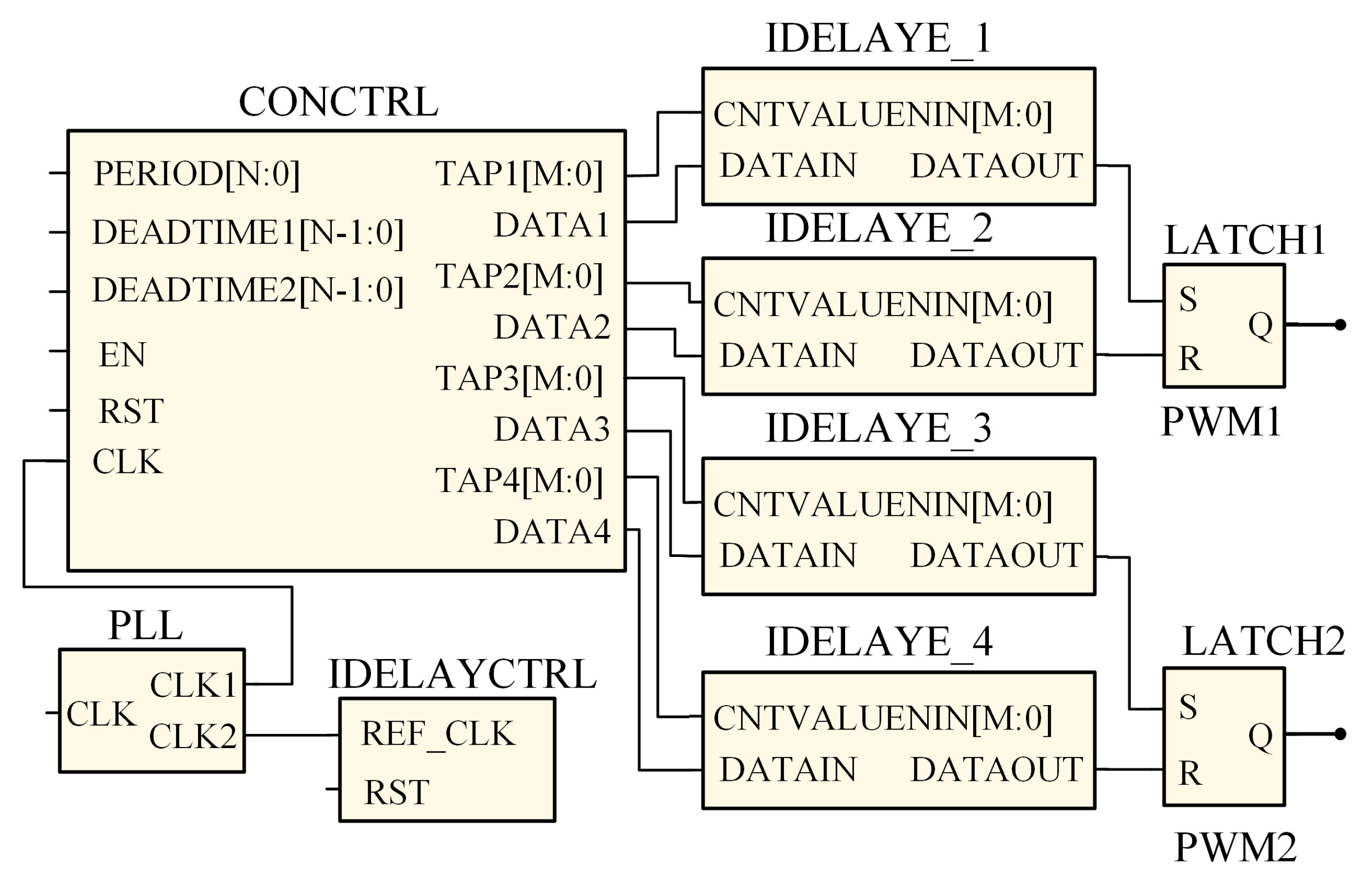
2.1. Digital Control Scheme
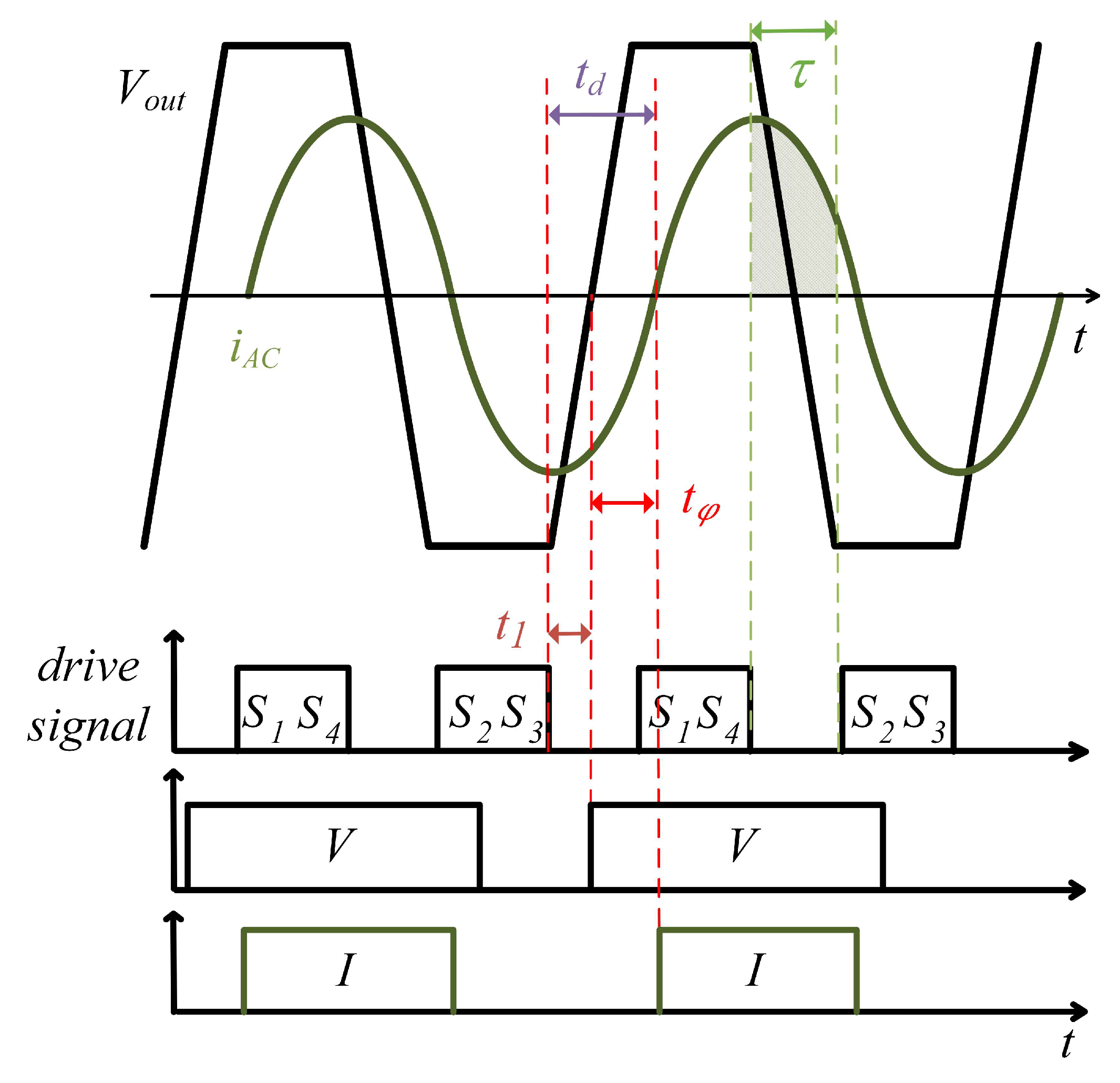
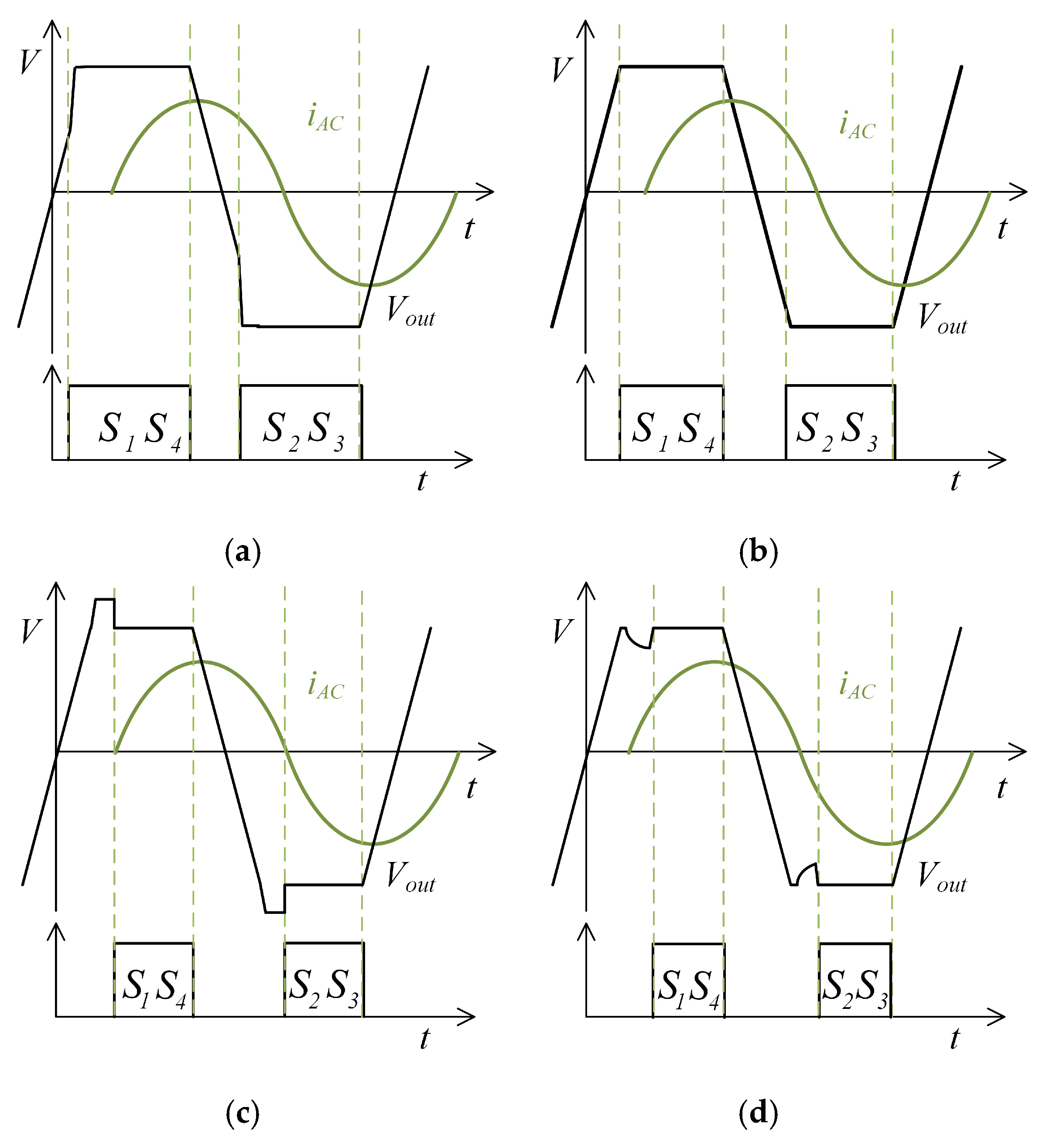
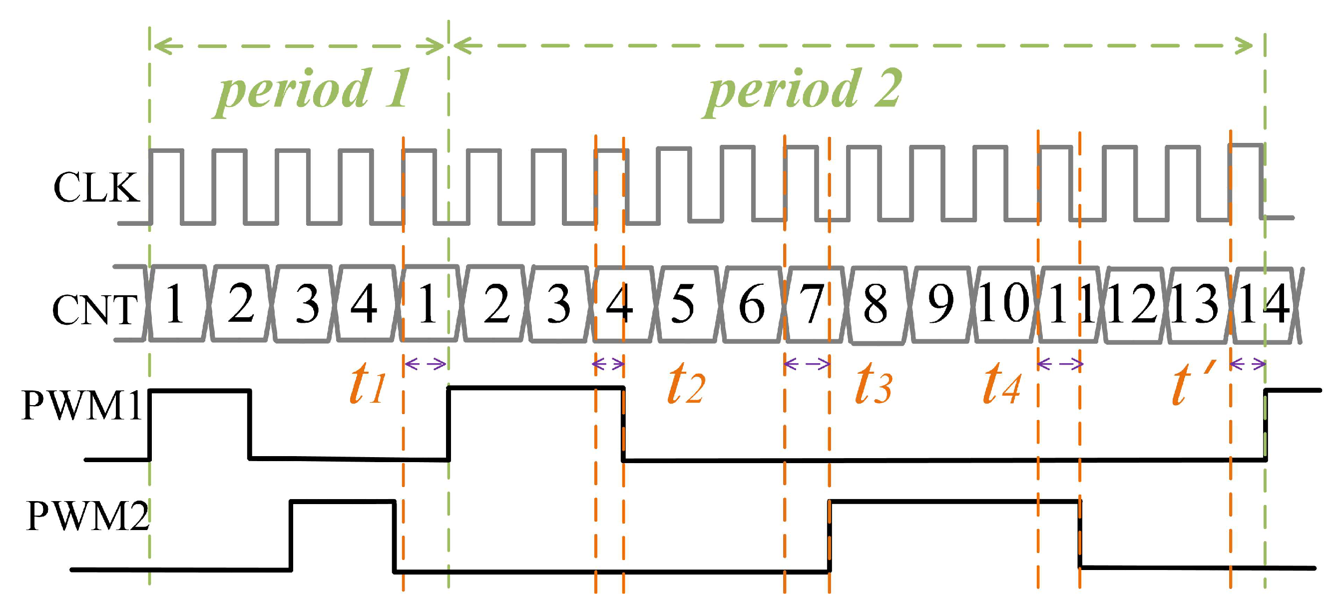
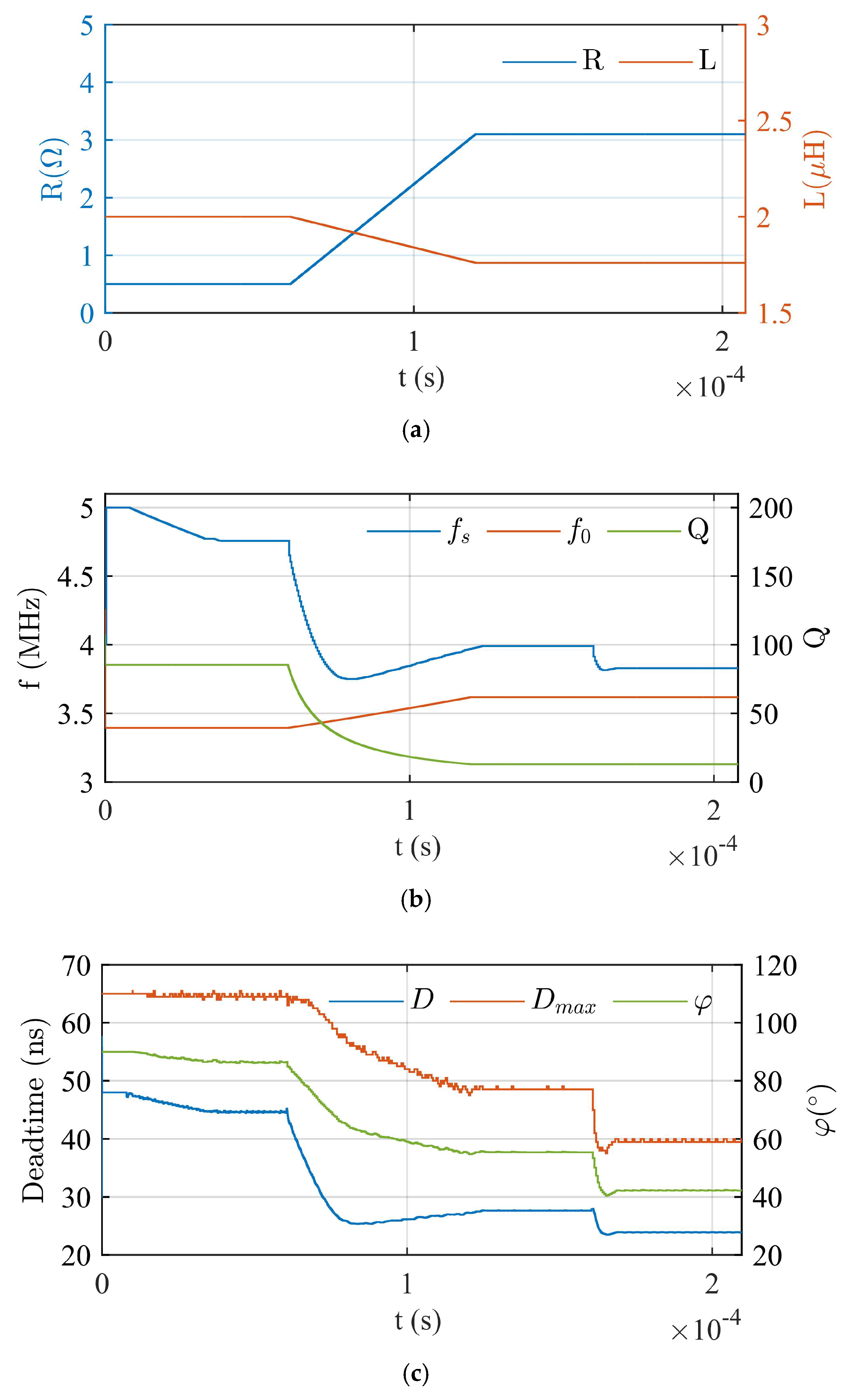
2.2. Dynamic Dead Time Calculation
3. High-Precision Digital Control Implementation Scheme
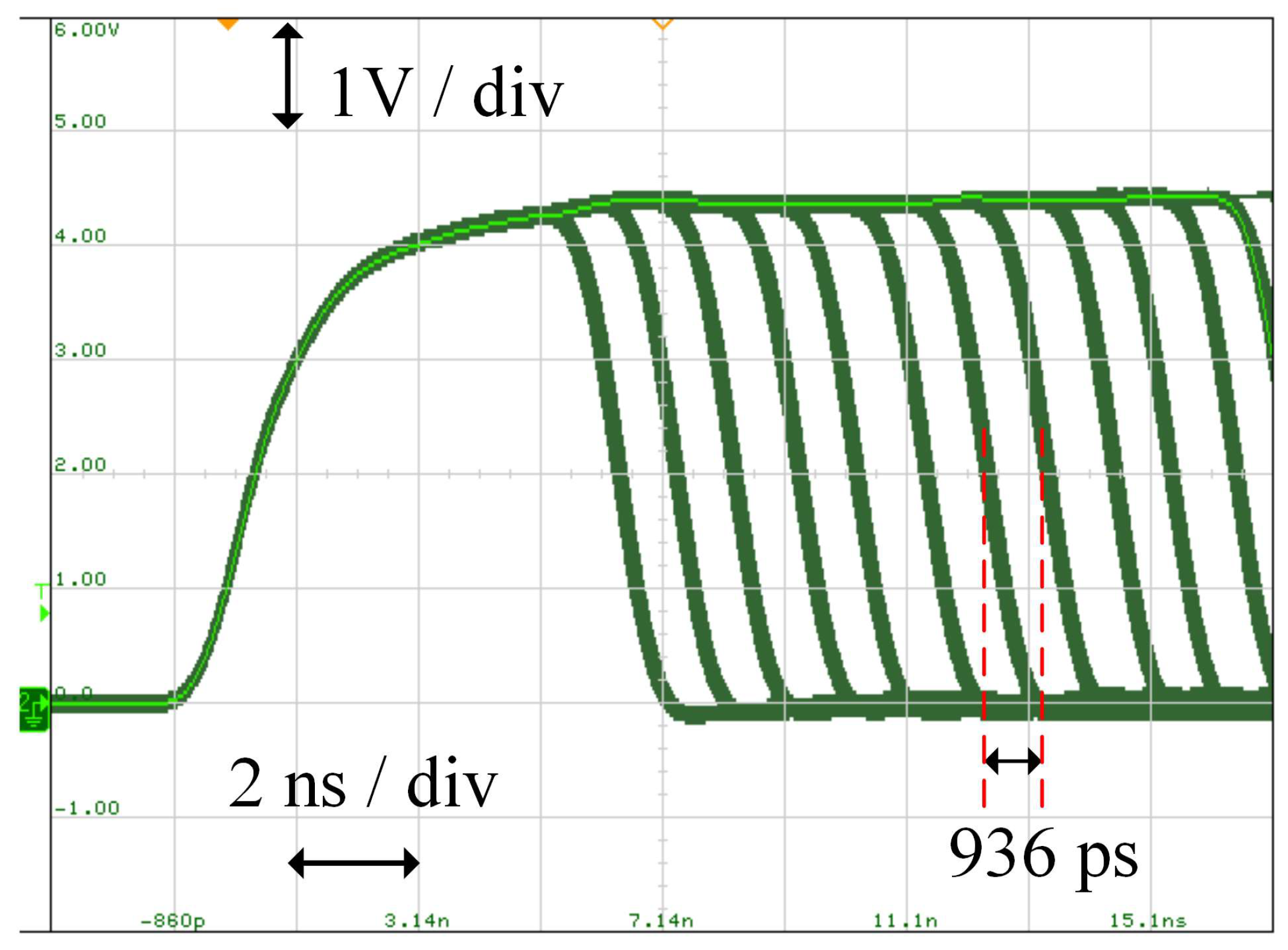
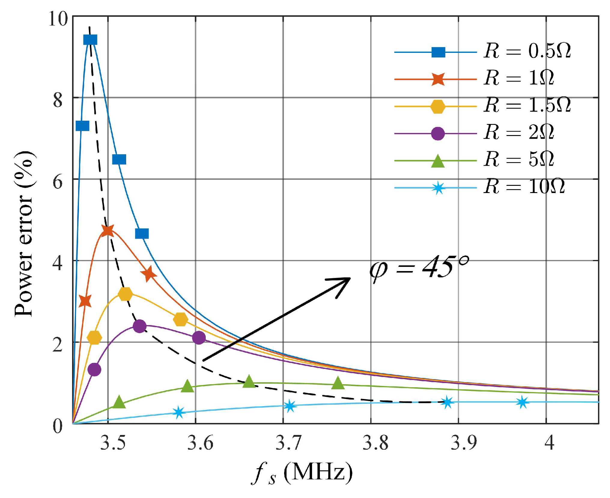
3.1. High-Precision DPFM Implementation Principle
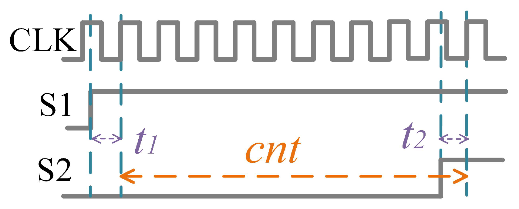
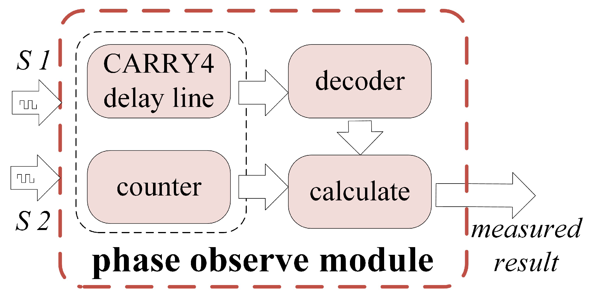
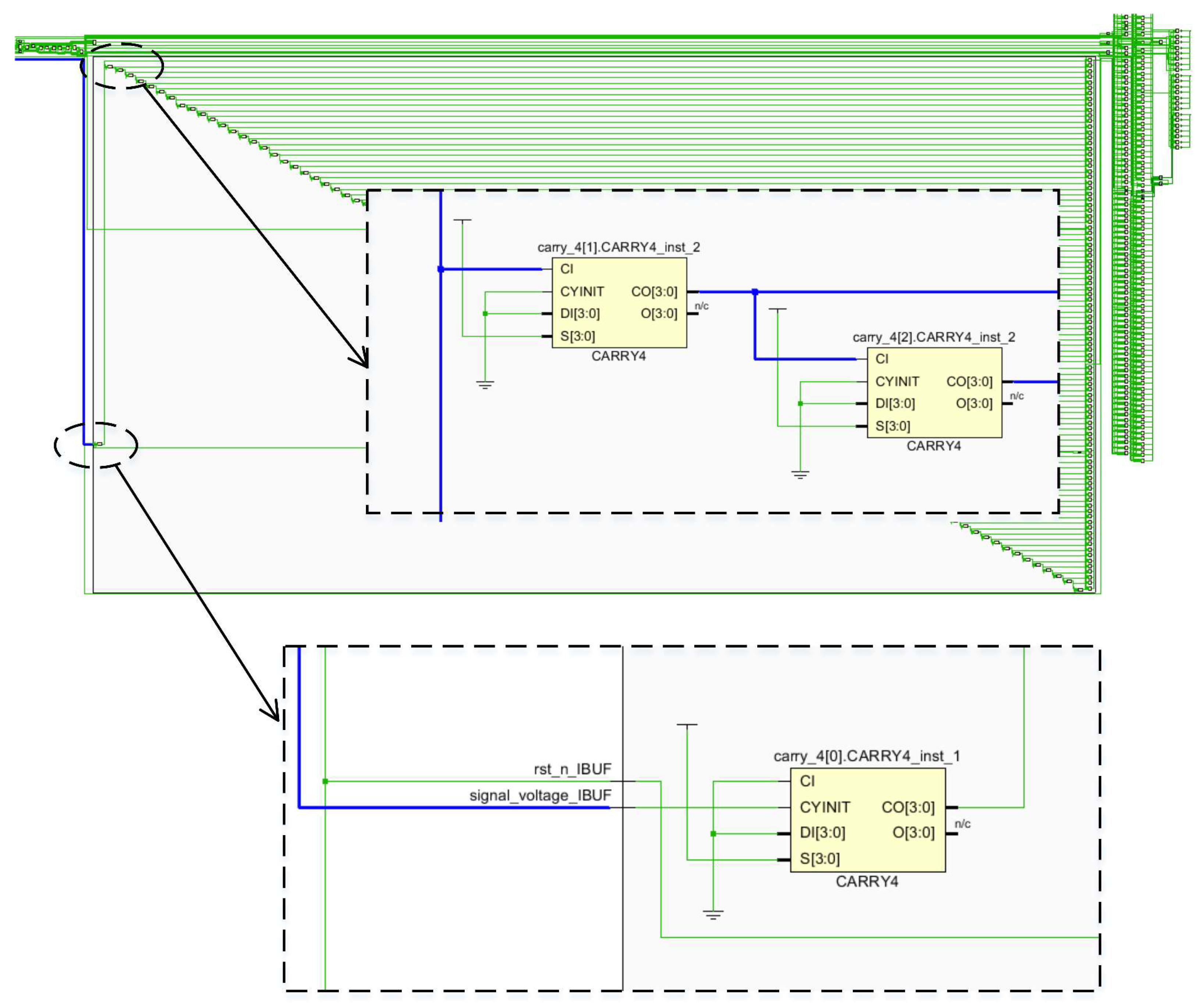
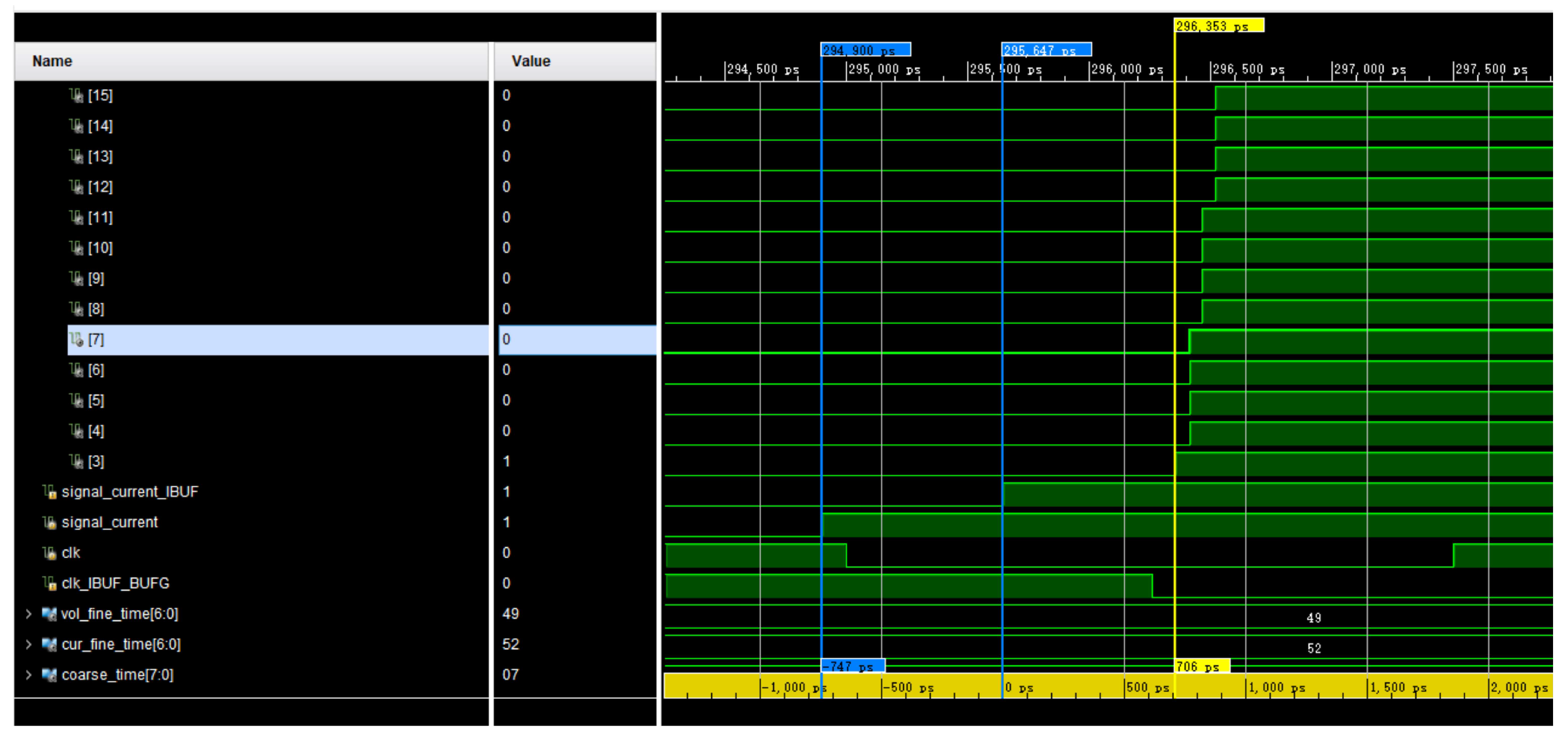
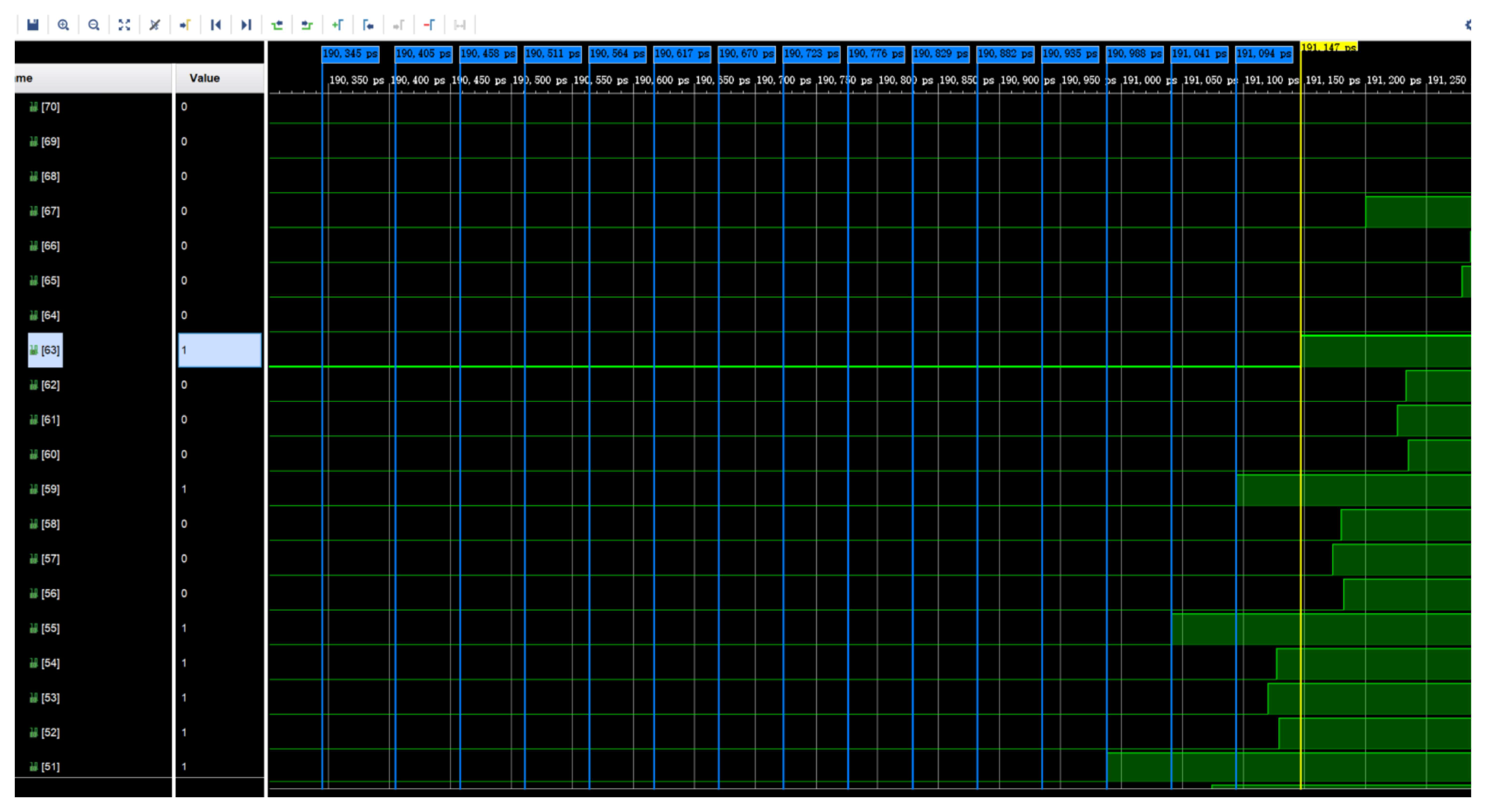
3.2. High-Precision Rapid Phase Measurement Implementation Scheme
3.3. Output Power Calculation
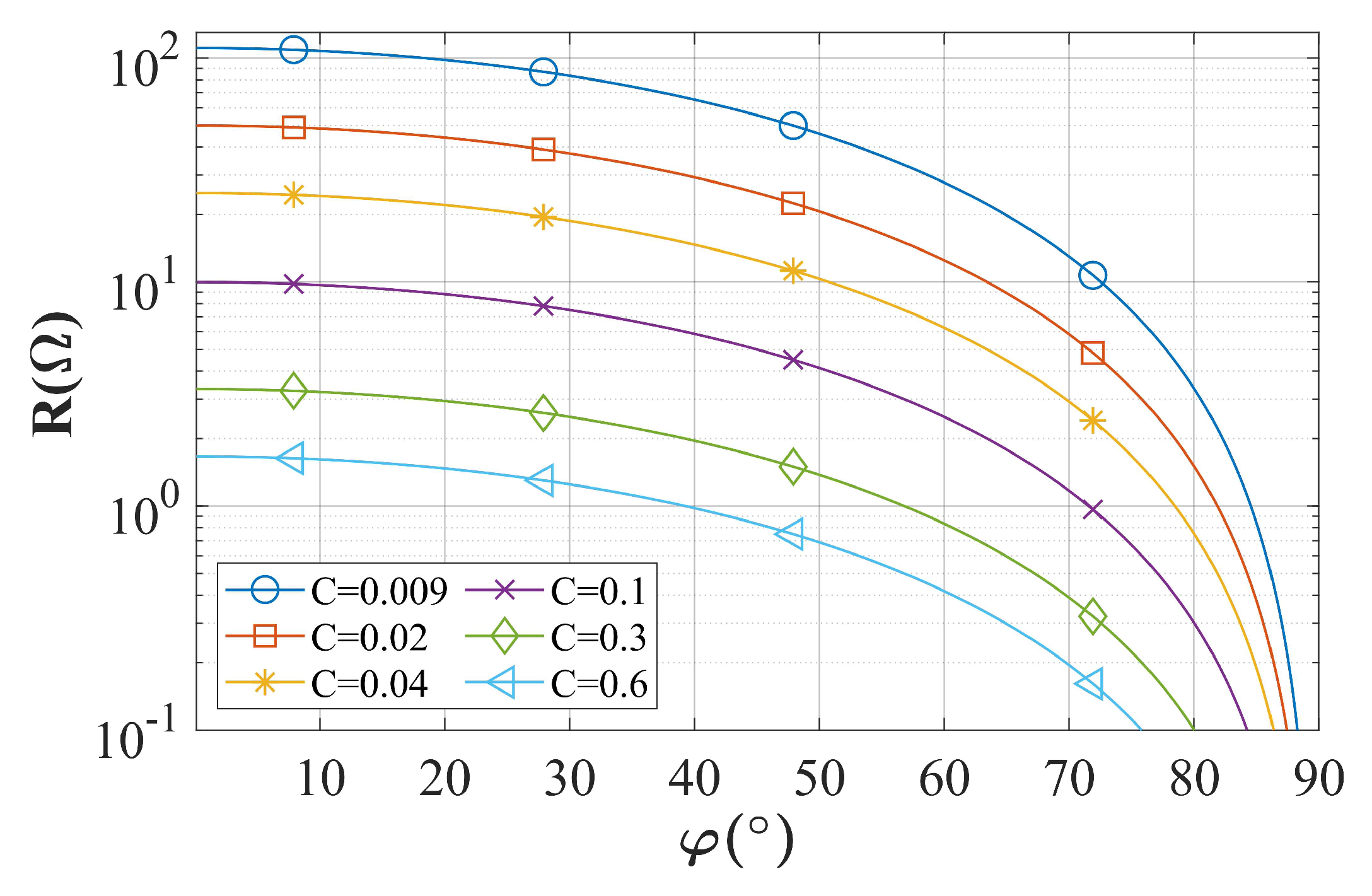
4. Simulation Analysis
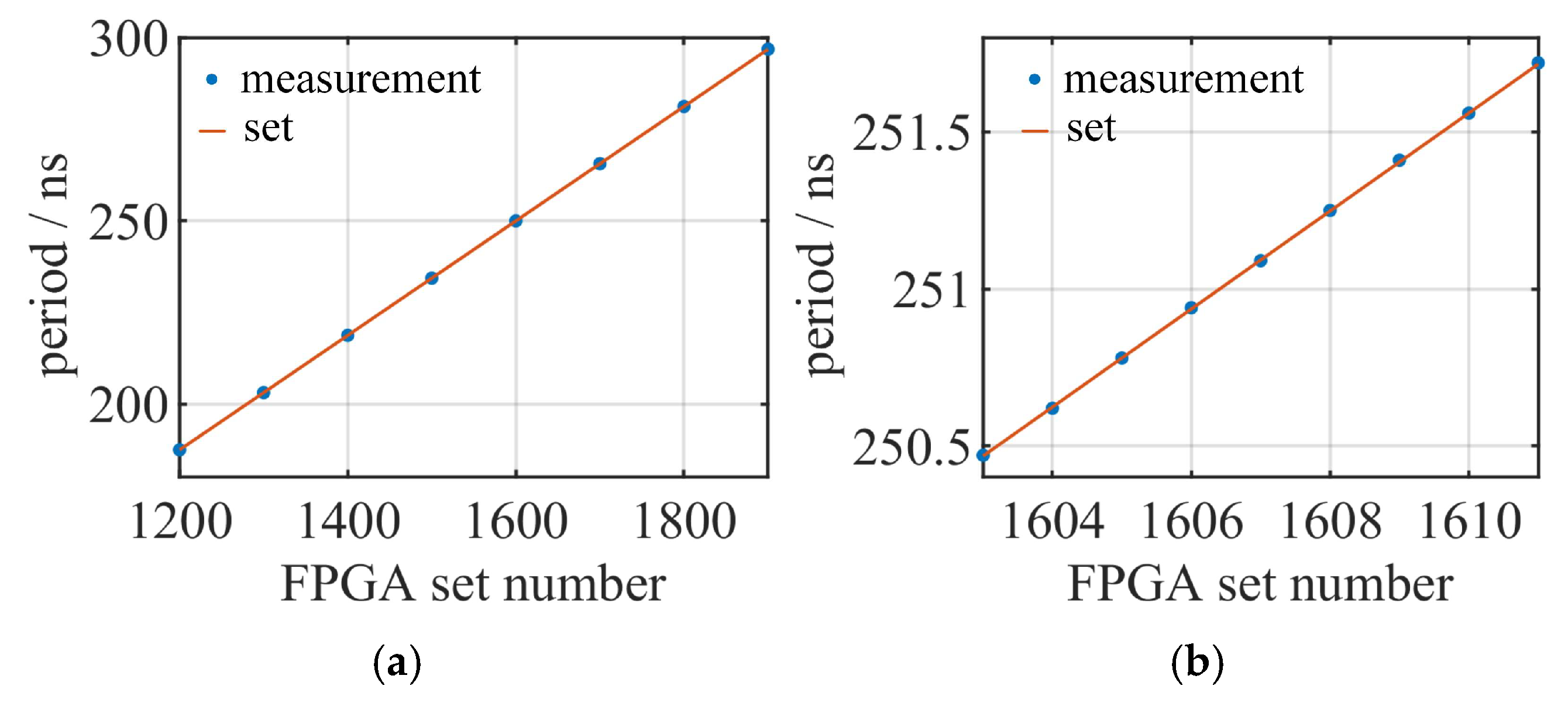
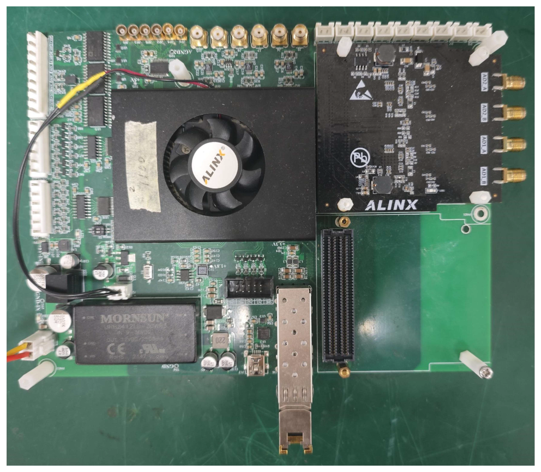
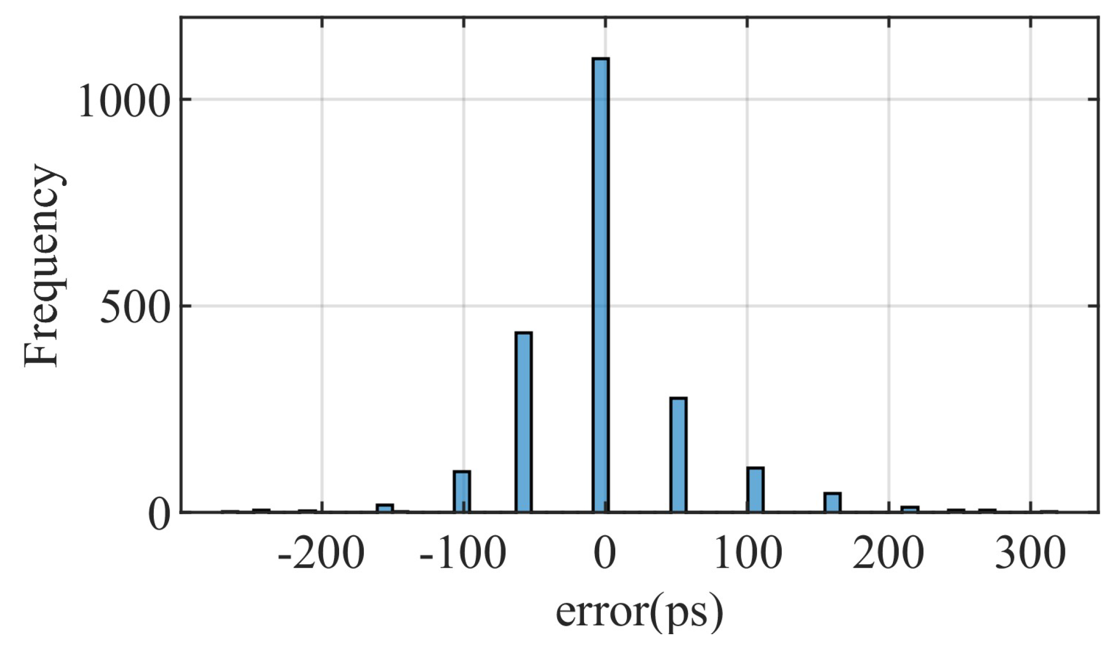
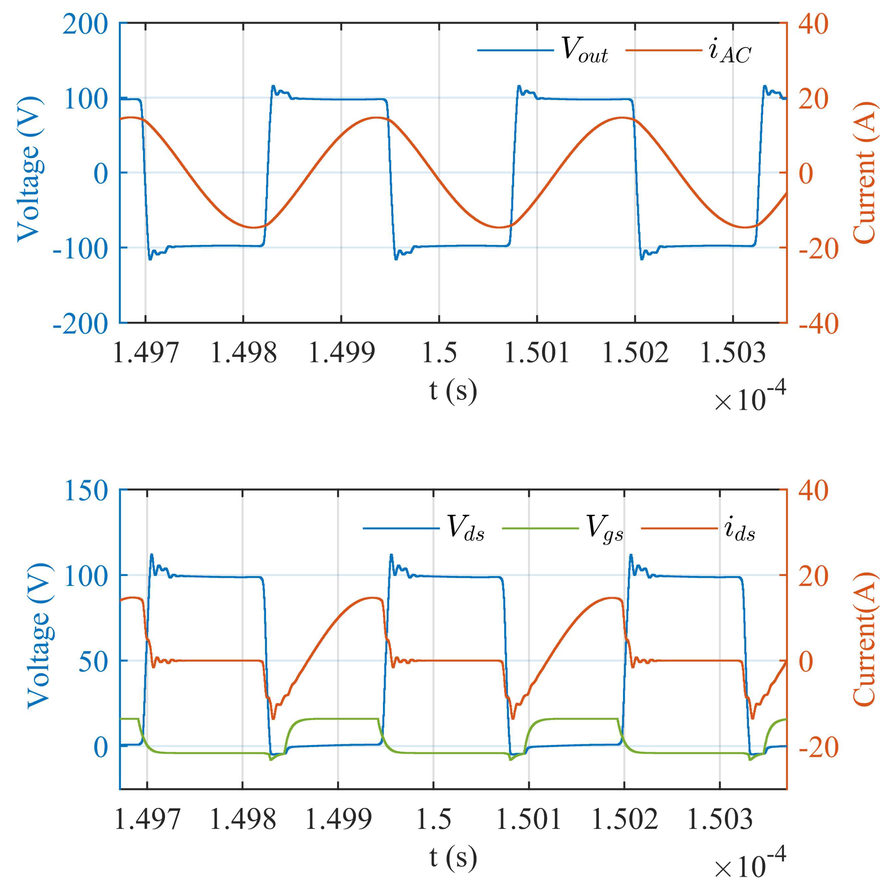
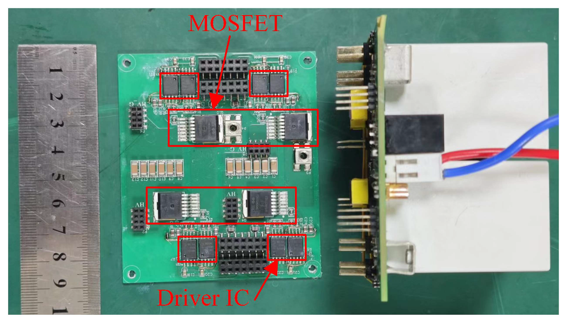
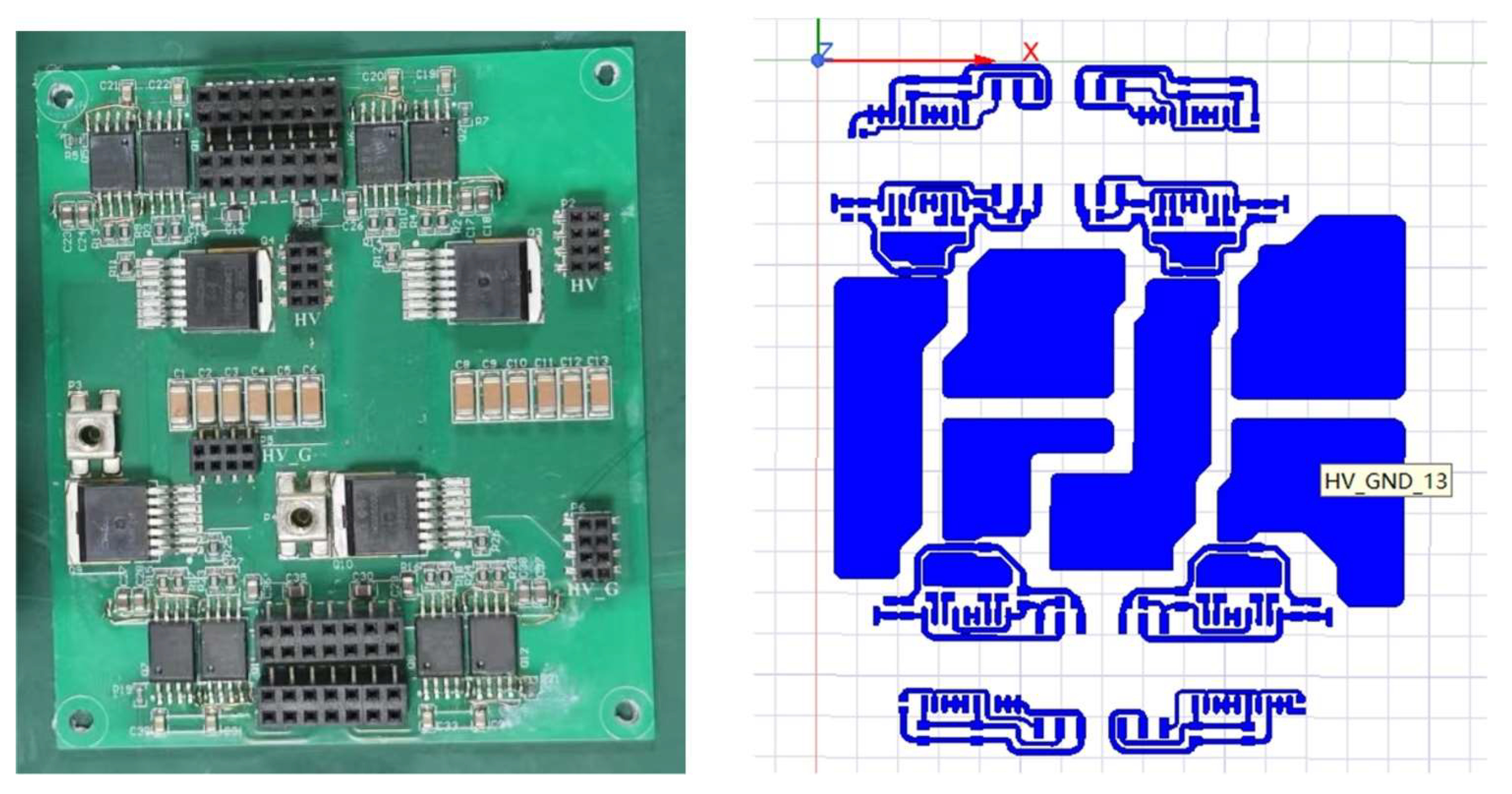
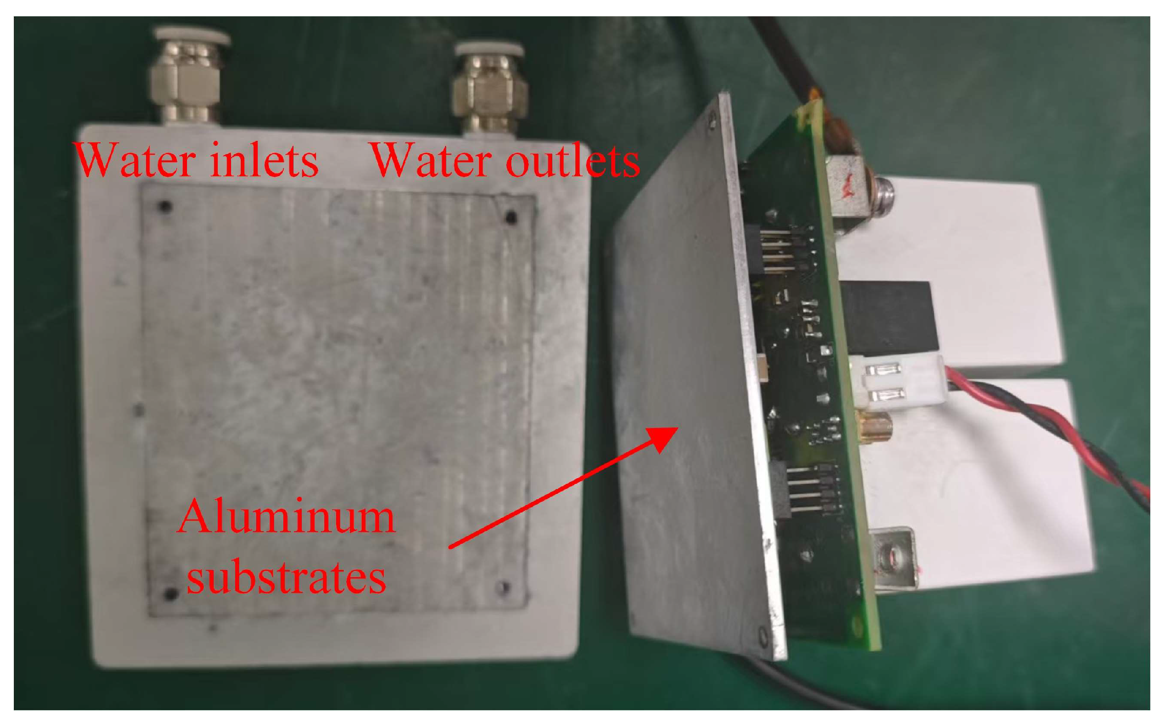
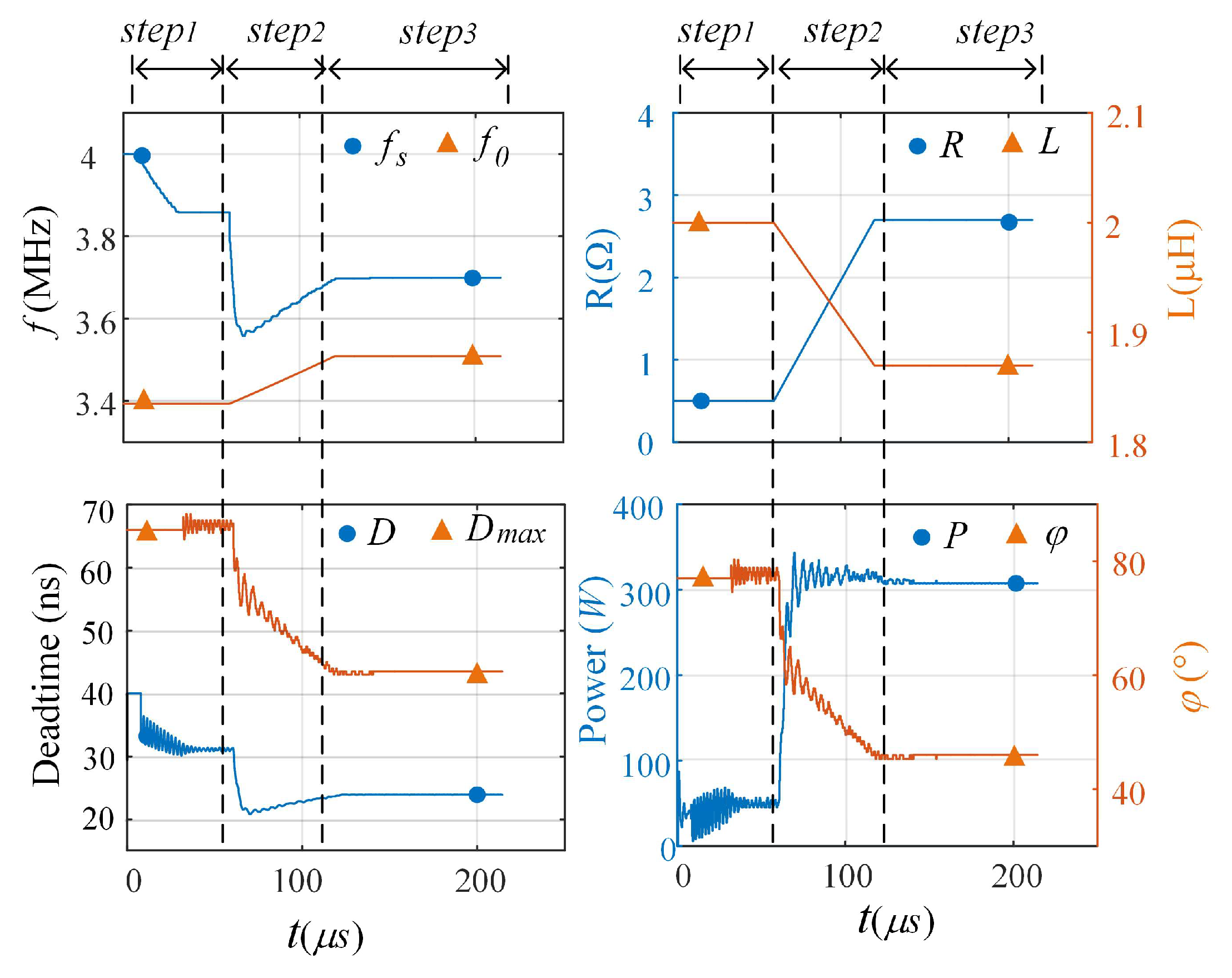
5. Experimental Results
6. Conclusions
Author Contributions
Funding
Data Availability Statement
Conflicts of Interest
References
- Wu, T.-F.; Duan, X.-M.; Wu, C.-P.; Hsu, W.-C. Design and Implementation of RF Resonant Inverter with Matching Circuit to Generate Plasma for Possible Endoscopy Sterilization. IEEE Trans. Plasma Sci. 2023, 51, 1045–1051. [Google Scholar] [CrossRef]
- Tao, X.; Bai, M.; Li, X.; Long, H.; Shang, S.; Yin, Y.; Dai, X. CH4–CO2 Reforming by Plasma—Challenges and Opportunities. Prog. Energy Combust. Sci. 2011, 37, 113–124. [Google Scholar] [CrossRef]
- Chabert, P.; Braithwaite, N. Inductively Coupled Plasmas. In Physics of Radio-Frequency Plasmas; Cambridge University Press: Cambridge, UK, 2011. [Google Scholar]
- Han, Y.; Radomski, A.; Chawla, Y.; Valcore, J.; Polizzo, S. Power Accuracy and Source-Pull Effect for a High-Power RF Generator. In Proceedings of the 2006 67th ARFTG Conference, San Francisco, CA, USA, 16 June 2006; pp. 81–92. [Google Scholar]
- Yoon, B.; Hwang, S.; Lee, S.; Jeong, B.; Kim, J.; Kim, S.; Kim, J. 4 MHz Electrosurgical Generator System for Wide Load Impedance Range with SiC-Based Full-Bridge Inverter. IEEE Trans. Ind. Electron. 2024, 71, 338–347. [Google Scholar] [CrossRef]
- Park, S.-H.; Sohn, Y.-H.; Cho, G.-H. SiC-Based 4 MHz 10 kW ZVS Inverter with Fast Resonance Frequency Tracking Control for High-Density Plasma Generators. IEEE Trans. Power Electron. 2020, 35, 3266–3275. [Google Scholar] [CrossRef]
- Al Bastami, A.; Jurkov, A.; Otten, D.; Nguyen, D.T.; Radomski, A.; Perreault, D.J. A 1.5 kW Radio-Frequency Tunable Matching Network Based on Phase-Switched Impedance Modulation. IEEE Open J. Power Electron. 2020, 1, 124–138. [Google Scholar] [CrossRef]
- Min, J.; Chae, B.; Suh, Y.; Kim, J.; Kim, H. Next-Generation Variable Capacitors to Reduce Capacitance Variable Time Using SiC MOSFETs and p-i-n Diodes in 13.56-MHz RF Plasma Systems. IEEE J. Emerg. Sel. Top. Power Electron. 2022, 10, 1353–1362. [Google Scholar] [CrossRef]
- Jurkov, A.S.; Radomski, A.; Perreault, D.J. Tunable Matching Networks Based on Phase-Switched Impedance Modulation. IEEE Trans. Power Electron. 2020, 35, 10150–10167. [Google Scholar] [CrossRef]
- Al Bastami, A.; Jurkov, A.; Gould, P.; Hsing, M.; Schmidt, M.; Ha, J.-I.; Perreault, D.J. Dynamic Matching System for Radio-Frequency Plasma Generation. IEEE Trans. Power Electron. 2018, 33, 1940–1951. [Google Scholar] [CrossRef]
- Han, Y.; Leitermann, O.; Jackson, D.A.; Rivas, J.M.; Perreault, D.J. Resistance Compression Networks for Radio-Frequency Power Conversion. IEEE Trans. Power Electron. 2007, 22, 41–53. [Google Scholar] [CrossRef]
- Barton, T.W.; Gordonson, J.M.; Perreault, D.J. Transmission Line Resistance Compression Networks and Applications to Wireless Power Transfer. IEEE J. Emerg. Sel. Top. Power Electron. 2015, 3, 252–260. [Google Scholar] [CrossRef]
- Liu, C.; Guan, Y.; Wang, Y.; Alonso, J.M.; Xu, D. Coordinate Compression Strategy of Resistance and Reactance for MHz-Range Inverter System. IEEE Trans. Power Electron. 2022, 37, 14993–15004. [Google Scholar] [CrossRef]
- YE, Z.; Rivas, J. Broadband High Frequency Power Conversion With Frequency-Tuning Matching Network. IEEE Open J. Power Electron. 2025, 6, 120–129. [Google Scholar] [CrossRef]
- Zhang, X.; Larson, L.E.; Asbeck, P.M.; Langridge, R.A. Analysis of Power Recycling Techniques for RF and Microwave Outphasing Power Amplifiers. IEEE Trans. Circuits Syst. II Analog. Digit. Signal Process. 2002, 49, 312–320. [Google Scholar] [CrossRef]
- Bogusz, A.; Lees, J.; Quaglia, R.; Watkins, G.; Cripps, S.C. Practical Load Compensation Networks in Chireix Outphasing Amplifiers Using Offset Transmission Lines. In Proceedings of the 2018 48th European Microwave Conference (EuMC), Madrid, Spain, 23–27 September 2018; pp. 17–20. [Google Scholar]
- Perreault, D.J. A New Architecture for High-Frequency Variable-Load Inverters. In Proceedings of the 2016 IEEE 17th Workshop on Control and Modeling for Power Electronics (COMPEL), Trondheim, Norway, 27–30 June 2016; pp. 1–8. [Google Scholar]
- Kumar, A.; Sinha, S.; Afridi, K.K. A High-Frequency Inverter Architecture for Providing Variable Compensation in Wireless Power Transfer Systems. In Proceedings of the 2018 IEEE Applied Power Electronics Conference and Exposition (APEC), San Antonio, TX, USA, 4–8 March 2018; pp. 3154–3159. [Google Scholar]
- Braun, W.D.; Perreault, D.J. A High-Frequency Inverter for Variable-Load Operation. IEEE J. Emerg. Sel. Top. Power Electron. 2019, 7, 706–721. [Google Scholar] [CrossRef]
- Zhang, H.; Al Bastami, A.; Jurkov, A.S.; Radomski, A.; Perreault, D.J. Multi-Inverter Discrete Backoff: A High-Efficiency, Wide-Range RF Power Generation Architecture. In Proceedings of the 2020 IEEE 21st Workshop on Control and Modeling for Power Electronics (COMPEL), Aalborg, Denmark, 9–12 November 2020; pp. 1–8. [Google Scholar]
- Liu, C.; Guan, Y.; Wang, Y.; Xu, D. Optimal Impedance Design for Dual-Branch High-Frequency Inverter Based on Active Regulation and Passive Projection. IEEE Trans. Power Electron. 2023, 38, 11183–11192. [Google Scholar] [CrossRef]
- Cabrera, S.E.; Gehring, T.; Denk, F.; Jin, Q.; Dycke, J.; Renschler, M.; Hiller, M.; Lemmer, U.; Kling, R. SiC-Based Resonant Converters with ZVS Operated in MHz Range Driving Rapidly Variable Loads: Inductively Coupled Plasmas as a Case of Study. IEEE Trans. Power Electron. 2022, 37, 7775–7788. [Google Scholar] [CrossRef]
- Eizaguirre, S.; Gehring, T.; Denk, F.; Simon, C.; Kling, R. Argon ICP Plasma Torch at Atmospheric Pressure Driven by a SiC Based Resonant Converter Operating in MHz Range. In Proceedings of the PCIM Europe Digital Days 2020, International Exhibition and Conference for Power Electronics, Intelligent Motion, Renewable Energy and Energy Management, online, 7–8 July 2020; pp. 1–8. [Google Scholar]
- Simon, C.; Eizaguirre, S.; Denk, F.; Heidinger, M.; Kling, R.; Heering, W. Control of a SiC 2.5 MHz Resonant Full-Bridge Inverter for Inductively Driven Plasma. In Proceedings of the PCIM Europe 2019; International Exhibition and Conference for Power Electronics, Intelligent Motion, Renewable Energy and Energy Management, Nuremberg, Germany, 7–9 May 2019; pp. 1–8. [Google Scholar]
- Ashraf, M.; Elserougi, A.A.; Okaz, A.M. Inductance Estimator-Based Resonance Frequency Tracking for Induction Heating Applications. In Proceedings of the 2021 22nd International Middle East Power Systems Conference (MEPCON), Assiut, Egypt, 14–16 December 2021; pp. 581–586. [Google Scholar]
- Tran, T.-V.; Chun, T.-W.; Lee, H.-H.; Kim, H.-G.; Nho, E.-C. PLL-Based Seamless Transfer Control Between Grid-Connected and Islanding Modes in Grid-Connected Inverters. IEEE Trans. Power Electron. 2014, 29, 5218–5228. [Google Scholar] [CrossRef]
- Hsieh, J.-C.; Lin, J.-L. Novel Single-Stage Self-Oscillating Dimmable Electronic Ballast with High Power Factor Correction. IEEE Trans. Ind. Electron. 2011, 58, 250–262. [Google Scholar] [CrossRef]
- Namadmalan, A.; Moghani, J.S. Tunable Self-Oscillating Switching Technique for Current Source Induction Heating Systems. IEEE Trans. Ind. Electron. 2014, 61, 2556–2563. [Google Scholar] [CrossRef]
- Belloumi, H.; Kourda, F. Double Modulation Technique for a ZVS Self-Oscillating Half-Bridge Inverter. IEEE Trans. Power Electron. 2015, 30, 1907–1913. [Google Scholar] [CrossRef]
- Zerehpoush, A.; Riazi Mobaraki, Z.; Afarideh, H.; Rahimpour, H. An Automatic Impedance Matching Network Based on Neural Network Technique for Inductive RF Plasma Source. IEEE Trans. Instrum. Meas. 2025, 74, 1–9. [Google Scholar] [CrossRef]
- Wolfspeed C3m0065090j. Available online: https://www.wolfspeed.com/products/power/sic-mosfets/900v-silicon-carbide-mosfets/c3m0065090j/ (accessed on 1 June 2019).
- Xu, L.; Lu, F.; Zhang, Z. Calculation of Dead Time in Full-Bridge Converters Considering MOSFET Parasitic Capacitance. In Proceedings of the Proceedings of 2023 International Conference on Wireless Power Transfer (ICWPT2023); Cai, C., Qu, X., Mai, R., Zhang, P., Chai, W., Wu, S., Eds.; Springer Nature: Singapore, 2024; pp. 189–196. [Google Scholar]
- Dahl, N.J.; Ammar, A.M.; Andersen, M.A.E. Identification of ZVS Points and Bounded Low-Loss Operating Regions in a Class-D Resonant Converter. IEEE Trans. Power Electron. 2021, 36, 9511–9520. [Google Scholar] [CrossRef]
- Shi, L.; Rodriguez, J.C.; Carrizosa, M.J.; Alou, P. ZVS Tank Optimization for Class-D Amplifiers in High Frequency WPT Applications. In Proceedings of the 2021 IEEE Applied Power Electronics Conference and Exposition (APEC), Phoenix, AZ, USA, 14–17 June 2021; pp. 1593–1598. [Google Scholar]
- De Rooij, M.A. The ZVS Voltage-Mode Class-D Amplifier, an eGaN FET-Enabled Topology for Highly Resonant Wireless Energy Transfer. In Proceedings of the 2015 IEEE Applied Power Electronics Conference and Exposition (APEC), Charlotte, NC, USA, 15–19 March 2015; pp. 1608–1613. [Google Scholar]
- Zhang, H.; Kou, B.; Jin, Y.; Zhang, H. Analysis of MOSFETs Switching Performance in Auxiliary Resonant Snubber Inverter. In Proceedings of the 2016 IEEE 8th International Power Electronics and Motion Control Conference (IPEMC-ECCE Asia), Hefei, China, 22–26 May 2016; pp. 1230–1235. [Google Scholar]
- Tebianian, H.; Salami, Y.; Jeyasurya, B.; Quaicoe, J.E. A 13.56-MHz Full-Bridge Class-D ZVS Inverter with Dynamic Dead-Time Control for Wireless Power Transfer Systems. IEEE Trans. Ind. Electron. 2020, 67, 1487–1497. [Google Scholar] [CrossRef]
- Lu, F.; Xu, L.; Zhang, Z. Analysis of the Parasitic Capacitance of MOSFET and Deadtime in High-Frequency ZVS Class-D Converters. In Proceedings of the 2024 IEEE 7th International Electrical and Energy Conference (CIEEC), Harbin, China, 10–12 May 2024; pp. 105–110. [Google Scholar]
- Lu, F.; Zhang, Z.-Q. A High-Precision and Wide-Range DPFM/DPWM Generation Method Using FPGA. Int. J. Circuit Theory Appl. 2025, 1–10. [Google Scholar] [CrossRef]
- Wang, Y.; Xie, W.; Chen, H.; Li, D.D.-U. Multichannel Time-to-Digital Converters With Automatic Calibration in Xilinx Zynq-7000 FPGA Devices. IEEE Trans. Ind. Electron. 2022, 69, 9634–9643. [Google Scholar] [CrossRef]
- Zhao, L.; Hu, X.; Liu, S.; Wang, J.; Shen, Q.; Fan, H.; An, Q. The Design of a 16-Channel 15 Ps TDC Implemented in a 65 Nm FPGA. IEEE Trans. Nucl. Sci. 2013, 60, 3532–3536. [Google Scholar] [CrossRef]
- Wu, J. Several Key Issues on Implementing Delay Line Based TDCs Using FPGAs. IEEE Trans. Nucl. Sci. 2010, 57, 1543–1548. [Google Scholar] [CrossRef]
- Xilinx 7 Series FPGAs Configurable Logic Block User Guide (UG474). Available online: https://docs.amd.com/r/en-US/ug474_7Series_CLB/Slice-Description (accessed on 1 April 2025).
- Wang, Y.; Kuang, J.; Liu, C.; Cao, Q. A 3.9-Ps RMS Precision Time-to-Digital Converter Using Ones-Counter Encoding Scheme in a Kintex-7 FPGA. IEEE Trans. Nucl. Sci. 2017, 64, 2713–2718. [Google Scholar] [CrossRef]
- Ye, Z.; Jain, P.K.; Sen, P.C. A Full-Bridge Resonant Inverter With Modified Phase-Shift Modulation for High-Frequency AC Power Distribution Systems. IEEE Trans. Ind. Electron. 2007, 54, 2831–2845. [Google Scholar] [CrossRef]
- Wang, Y.; Kheirollahi, R.; Lu, F.; Zhang, H. Exploring Switching Limit of SiC Inverter for Multi-kW Multi-MHz Wireless Power Transfer System. In Proceedings of the 2023 IEEE Applied Power Electronics Conference and Exposition (APEC), Orlando, FL, USA, 19 March 2023; pp. 2952–2957. [Google Scholar]


| Paper | Time | Frequency | Power | Topology | Efficiency | Features |
|---|---|---|---|---|---|---|
| [4] | 2006 | 13.56 MHz | 3 kW | Class E | NA | Impedance matching network, multiple power amplifiers. |
| [5] | 2024 | 3.5 MHz, 4 MHz | 200 W | Class D | >60% | In the impedance matching network, fixed-value passive components are used. With a fixed input voltage, the output power is controlled through duty cycle adjustment. |
| [30] | 2025 | NA | NA | NA | NA | Using the Neural Network Technique for the impedance matching network. |
| [7] | 2020 | 13.56 MHz | 1.5 kW | NA | >60% | Phase-switched impedance modulation; impedance matching is achieved within tens of microseconds. |
| [8] | 2022 | 13.56 MHz | 1 kW | NA | NA | By utilizing SiC MOSFETs and p-i-n diodes to construct electronic capacitors in place of vacuum capacitors, the impedance matching time is significantly reduced to the order of a few milliseconds. |
| [10] | 2017 | 13.56 MHz | 250 W | NA | NA | Using a Resistance Compression Network, an impedance transformation stage, and a specially configured set of plasma drive coils to achieve rapid adjustment to plasma load variations. |
| [19] | 2019 | 13.56 MHz | 1 kW | Class D | 95.4% | Using two RF power amplifiers with independently controllable amplitude and phase, compressing the impedance seen by each inverter. |
| [6] | 2019 | 4 MHz | 10 kW | Class D | 97% | Output power is adjusted by modifying the switching frequency, and high-resolution resonant frequency tracking control is implemented using analog techniques. |
| [22] | 2022 | 3 MHz | 25 kW | Class D | 94% | Analyzing the characteristics of load variation in ICP during plasma generation. |
Disclaimer/Publisher’s Note: The statements, opinions and data contained in all publications are solely those of the individual author(s) and contributor(s) and not of MDPI and/or the editor(s). MDPI and/or the editor(s) disclaim responsibility for any injury to people or property resulting from any ideas, methods, instructions or products referred to in the content. |
© 2025 by the authors. Licensee MDPI, Basel, Switzerland. This article is an open access article distributed under the terms and conditions of the Creative Commons Attribution (CC BY) license (https://creativecommons.org/licenses/by/4.0/).
Share and Cite
Lu, F.; Zhang, Z. Digital Control Scheme for Class-D Power Amplifier Driving ICP Load Without Matching Network. Energies 2025, 18, 2385. https://doi.org/10.3390/en18092385
Lu F, Zhang Z. Digital Control Scheme for Class-D Power Amplifier Driving ICP Load Without Matching Network. Energies. 2025; 18(9):2385. https://doi.org/10.3390/en18092385
Chicago/Turabian StyleLu, Fuchao, and Zhengquan Zhang. 2025. "Digital Control Scheme for Class-D Power Amplifier Driving ICP Load Without Matching Network" Energies 18, no. 9: 2385. https://doi.org/10.3390/en18092385
APA StyleLu, F., & Zhang, Z. (2025). Digital Control Scheme for Class-D Power Amplifier Driving ICP Load Without Matching Network. Energies, 18(9), 2385. https://doi.org/10.3390/en18092385