1. Introduction
Higher power density and enhanced efficiency remains a central objective in the development of modern rail traction systems [
1]. As the core component of these systems, the traction converter must deliver increased power output and improved control performance, all within the constraints of a fixed installation space. These demands become increasingly critical as the speed class of rail vehicles continues to advance, necessitating innovative solutions to meet both performance and spatial requirements [
2].
Traction converters currently rely predominantly on two-level inverter topologies, which are constrained by low switching frequencies. This limitation leads to suboptimal harmonic performance and poses significant challenges in improving power density and control precision. In contrast, three-level inverters offer notable advantages, including reduced voltage stress on switching devices, diminished output harmonics, and enhanced power density and efficiency. As a result, they have emerged as a focal point of research in power electronics converters [
3,
4]. The neutral point clamped (NPC) inverter, a widely adopted three-level topology, has been deployed in Japan’s Shinkansen trains and subsequently introduced in China for use in CRH2 trains. By incorporating an additional zero-vector conduction path, NPC inverters achieve significantly improved harmonic performance compared to two-level inverters [
5]. However, a critical drawback arises during transitions between zero-vector and effective-vector outputs: the inner switching devices operate at twice the switching frequency of the outer devices. This results in concentrated thermal stress on the inner devices, and without meticulous thermal management, their failure could compromise the entire converter module [
6,
7,
8].
To address these challenges, the active neutral point clamped (ANPC) topology replaces the diodes in the NPC structure with controllable switching devices [
9]. This innovation enables more uniform loss distribution, thereby enhancing system efficiency and power density while mitigating the thermal imbalance that limits the lifespan of NPC-based converters [
10]. In the context of traction converters, ANPC topology offers significant benefits, including simplified thermal design, improved power density and efficiency, and extended operational lifespan, positioning it as a promising solution for next-generation rail systems [
11].
High-power medium-voltage three-level inverters are characterized by significant switching losses [
12]. To enhance equipment utilization and overall inverter efficiency, the maximum permissible switching frequency (
fsw) is typically constrained to only a few hundred hertz [
13]. Given the wide operating frequency range of the motor, the pulse ratio P (defined as the ratio of
fsw to the fundamental frequency
fe, P =
fsw/
fe) exhibits substantial variation across the entire speed range. At medium-to-high speeds, conventional asynchronous modulation can lead to elevated harmonic distortion when the pulse count is low.
Synchronous pulse-width modulation (PWM) has emerged as an effective strategy for mitigating harmonic distortion under such conditions. With its inherent synchronicity and symmetry, synchronous PWM is particularly advantageous in scenarios where the pulse count P falls below 21. To further optimize the control performance of high-power adjustable-speed drives, multimode modulation strategies are often employed [
14].
Among the techniques such as synchronous sinusoidal PWM (SPWM), synchronous space vector PWM (SVPWM), selective harmonic elimination PWM (SHEPWM), and current harmonic minimization PWM (CHMPWM), the synchronous SVPWM offers a more practical alternative, as it can be readily implemented online using digital processors [
15]. Moreover, synchronous SVPWM provides flexibility in adjusting sampling points and switching sequences, making it a highly adaptable solution for real-time control in high-power inverter systems [
16].
The insulated gate bipolar transistor (IGBT) serves as the core power conversion device within converter modules, and its junction temperature control is critical for enhancing converter reliability and extending device lifespan [
17]. Active junction temperature control involves two primary steps: junction temperature estimation and active regulation [
18]. While significant progress has been made in the estimation of IGBT junction temperature [
19], research on active temperature equalization control in active neutral point clamped (ANPC) inverters, particularly within the context of rail transportation, remains limited. Previous studies have explored various approaches to optimize inverter performance. For instance, one study [
20] proposed reducing total switching losses by optimally combining two modulation modes within a calculation cycle. However, this method falls short of achieving true active junction temperature equalization between inner and outer switching devices. Another study [
21] employed different thermal control strategies at varying switching frequencies, adjusting the frequency based on junction temperature. However, the asynchronous modulation scheme developed in this work is not entirely suited for the specific demands of rail transit applications [
22].
In addition, wide-bandgap semiconductors such as SiC and GaN have been utilized to achieve loss reduction/balancing [
23,
24]. In [
25], a “SiC + Si” hybrid three-level ANPC converter was proposed to minimize losses. This topology employs four SiC devices operating at the carrier frequency and two Si devices operating at the fundamental frequency. However, hardware-based thermal control improvements inevitably introduce additional costs and design complexity. Consequently, control/modulation enhancements remain more attractive. Among these, adjusting switching frequency represents a common approach. In [
26], the switching frequency is dynamically modulated based on the system’s output power level to mitigate temperature fluctuations. However, this method can only balance the average temperature of the inverter over extended time scales, without addressing the instantaneous temperature imbalance among switching devices. The inherent complexity of ANPC topology and its modulation presents additional challenges. Conventional vector-based modulation schemes are often inadequate for rail transit, where multi-dimensional real-time constraints must be simultaneously managed. These constraints include balancing midpoint potential, equalizing switching device losses, and actively controlling junction temperature. Developing an effective modulation strategy that addresses these interrelated requirements remains a key research challenge in advancing ANPC inverters for rail transportation.
In this study, we address the challenge of junction temperature equalization in three-level traction inverters. First, based on the active neutral point clamped (ANPC) topology, we derive precise loss quantification equations for both switching and conduction losses. Next, leveraging the distinct zero-vector commutation paths inherent to the ANPC topology, we establish the relationship between the loss prediction model and the corresponding switching vectors. To tackle this as a multi-objective optimization problem, we develop a loss equalization modulation strategy incorporating a closed-loop control of temperature rise. Recognizing that midpoint potential balance poses a relatively weak constraint in certain scenarios, we prioritize the design of a modulation strategy that ensures loss equalization among the power devices within each bridge arm. This is achieved while maintaining midpoint voltage stability and delivering high-quality output power. Finally, the proposed strategy is rigorously validated through both simulation and experimental testing, demonstrating its feasibility and effectiveness in improving the thermal balance and overall performance of the traction inverter.
2. Mathematical Model and Synchronous SVPWM
2.1. ANPC Inverter Topology and Switching States
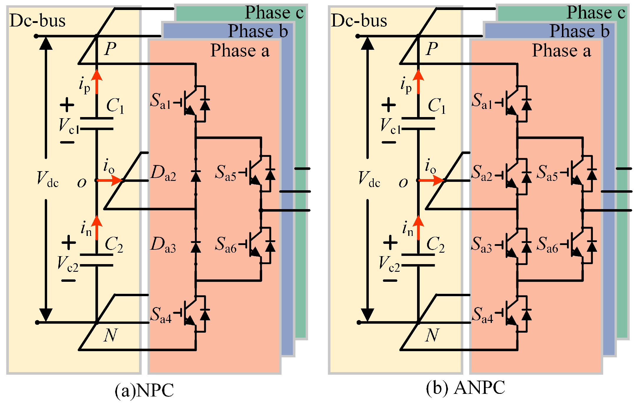
The circuit topologies of the three-phase 3L-NPC and 3L-ANPC inverters are shown in
Figure 1a,b, respectively, where
Vdc is the dc-link voltage distributed in two dc-link capacitors, C
1 and C
2. Compared with the NPC topology, two new power devices are added in the ANPC topology instead of the two clamping diodes in the NPC topology. At the output O level, for example, in the A phase, there are two channels in the ANPC topology, which are the upper channel and the lower channel, and the appropriate channel can be flexibly selected without them. It is possible to flexibly select the appropriate channel to balance the switching losses of each switching device without affecting the quality of the output voltage.
The circuit topologies of the three-phase three-level neutral point clamped (3L-NPC) and active neutral point clamped (3L-ANPC) inverters are depicted in
Figure 1a,b, respectively. In both configurations, the DC-link voltage Vdc is distributed across two DC-link capacitors, C
1 and C
2.
ip and
in are the current flowing through capacitors C
1 and C
2 respectively, and
io is the current flowing out of the neutral point. Compared to the NPC, the ANPC introduces two additional controllable power devices, replacing the two clamping diodes present in the NPC structure.
In the ANPC three-level topology, each phase bridge arm consists of six power devices, theoretically allowing for 64 possible switching states per phase. However, to ensure the safe operation of the inverter, certain switching combinations must be avoided. Specifically, configurations that result in half-bus or full-bus conduction pose a significant risk, as they can lead to short-circuit conditions or expose devices to voltages exceeding their rated limits. To mitigate these risks, only six permissible switching state combinations are used. For an output voltage of zero, six distinct switching states are available: OU1, OU2, OU3, OL1, OL2 and OL3. The conduction status of the power devices corresponding to each switching state is detailed in
Table 1. These selected states ensure safe and reliable inverter operation while maintaining the necessary output voltage characteristics.
2.2. Synchronize SVPWM
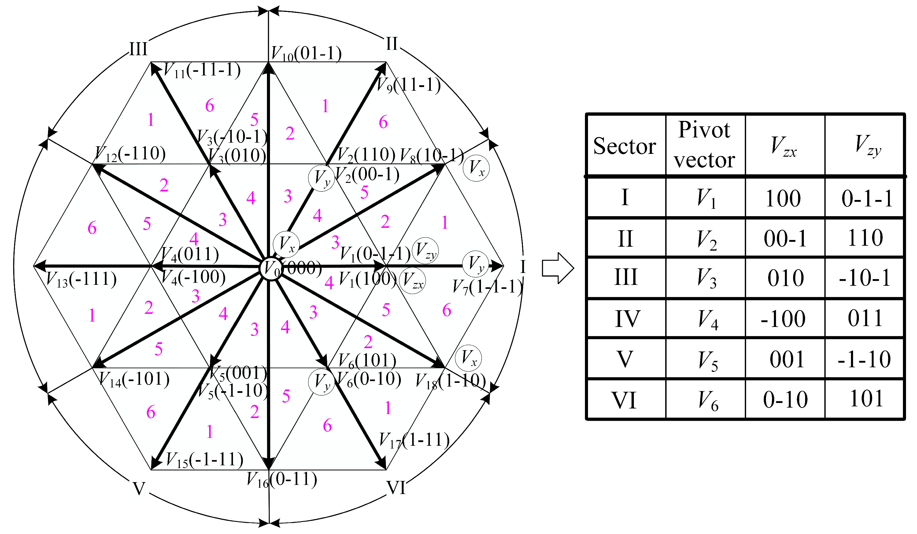
As illustrated in
Figure 2, the synchronous space vector pulse-width modulation (SVPWM) method partitions the space vector plane into six sectors (I–VI), and each sector is divided into six smaller sectors (1–6). To ensure symmetry in the output voltage waveforms, the reference vectors are uniformly distributed within each sector. The distribution of reference vectors in Sector I is depicted in
Figure 3. In this scheme,
N represents the total number of reference vectors within each sector. When
N is odd, the n-th reference vector aligns with the boundary between adjacent sectors, while the remaining reference vectors are positioned entirely within the sector. Conversely, when NNN is even, all reference vectors are confined within the sector. The angular spacing between consecutive reference vectors is consistently maintained at π/(3
N), ensuring uniform modulation and high-quality output voltage.
In the three-level inverter synchronous space vector modulation (SSVM) scheme, the reference vector is synthesized using the nearest three basic vectors. To facilitate analysis, the basic vectors within each sector are redefined. Specifically, the positive and negative small vectors located at the center of each sector are designated as Vzx and Vzy, respectively. For the remaining basic vectors in each sector, only a single switching state, Vx or Vy, is defined, distinguished from Vzx or Vzy. This redefinition simplifies the modulation process while maintaining the necessary precision for generating the reference vector.
Taking I as an example, the redefined fundamental vector is shown in
Figure 2. According to the ‘volt-second’ principle of equilibrium, the action time of the basic vector can be calculated as follows:
Here, Vref represents the reference vector and Ts denotes the sampling period. The operation times of the basic vectors Vx and Vy are given by Tx and Ty, respectively. Meanwhile, Tz corresponds to the total action duration of the small vectors Vzx and Vzy.
Synchronous SVPWM imposes synchronization, total pulse symmetry (TPS), and half-wave symmetry (HWS) as essential constraints, while quarter-wave symmetry (QWS) is considered non-essential. To ensure both synchronization and waveform symmetry, the design of the switching sequence must comply with the restriction conditions outlined in
Table 2 [
9]. Each switching state is either labeled or unlabeled, with complementary relationships defined between them. Specifically, the complementary state of “state 2” is “state 0”, and vice versa. For “state 1”, the complementary state is identical to itself. These complementary rules are integral to achieving the required symmetry and maintaining waveform quality under the SVPWM scheme.
To reduce switching frequency, two essential conditions must be considered in the design of the switching sequence. First, during transitions between voltage vectors, only a single switch in one phase should change state. Second, the initial vector of the current sampling interval must match the final vector of the previous sampling interval, ensuring continuity. In the case of synchronous SVPWM, switching sequences that adhere to these conditions can be categorized into three distinct groups. These classifications provide a structured framework for achieving low switching losses while maintaining high-quality waveform performance.
The design of switching sequences needs to ensure that the switching states satisfy the restrictions listed in
Table 3. The symbol ‘→’ denotes that switching can only occur in one direction, while ‘↔’ indicates that switching is possible in both directions.
The relationships among
N, δ, ε and P are summarized in
Table 4, where δ denotes the number of switches per sampling cycle and ε corresponds to the number of additional switches generated during sector switching.
The phase voltages of each switching sequence of the synchronous SVPWM satisfy the synchronization, TPS, and HWS, but the QWS exists only in type I and type III.
3. Proposed Active Thermal Control Method
3.1. Analysis of Inverter Mode of Three-Level ANPC
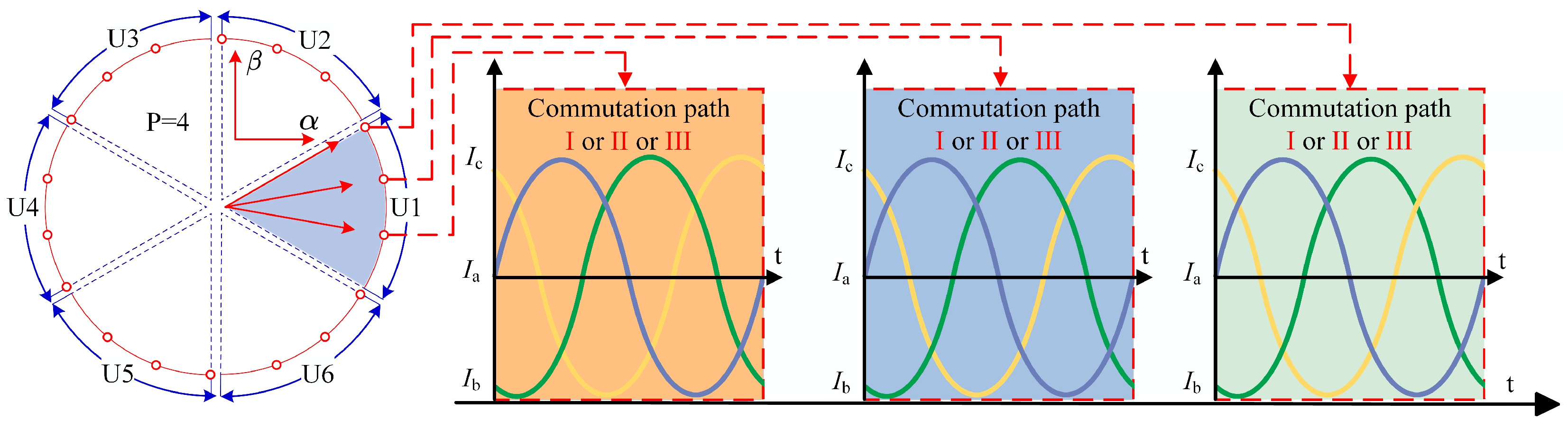
The 3L-ANPC inverter, due to the presence of redundant zero vectors, offers multiple commutation paths and operates in three typical modes, as depicted in
Figure 3.
In Operation Mode I, switching occurs between vectors P and OL2 during the positive half-cycle and between vectors NNN and OU2 during the negative half-cycle. In this mode, switches Sx2 and Sx3 operate at a high switching frequency, while switches Sx1, Sx4, Sx5, and Sx6 operate at a lower frequency. As a result, the primary switching losses are concentrated on Sx2 and Sx3.
In Operation Mode II, switching occurs between vectors P and OU1 during the positive half-cycle and between vectors N and OL1 during the negative half-cycle. This configuration ensures that current commutation takes place within a single module, reducing the impact of stray currents. In this mode, switches Sx2 and Sx3 operate at the fundamental frequency, while the remaining switches operate at a higher frequency. Notably, switches Sx5 and Sx6 are switched at a higher frequency than Sx1 and Sx4, which helps to balance the losses across the six switching devices in each phase.
In Operation Mode III, switching occurs between vectors P and OU2 during the positive half-cycle and between P and OL2 during the negative half-cycle. In this mode, the majority of the commutation losses are concentrated within the high-frequency unit modules Sx1, Sx4, Sx5, and Sx6. Meanwhile, switches Sx2 and Sx3 operate at the industrial frequency only during voltage commutation, effectively avoiding current commutation between different unit modules. This reduces the detrimental effects of parasitic inductance on switching speed. The theoretical loss distribution for this commutation path is more balanced, resulting in improved thermal characteristics compared to the larger commutation loops found in other modes.
The choice of current commutation method significantly influences the balanced distribution of power device losses and junction temperatures within the three-level ANPC converter. By selecting an appropriate commutation strategy, it is possible to achieve a more uniform distribution of losses and better thermal management across the power devices. As an example,
Figure 4 shows the form in which PWMI and PWMII and PWMIII are mixed in a 1:1:1 ratio across the three sampling points of sector U1, where the red arrow represents the voltage reference vector corresponding to the sampling point.
3.2. Online Calculation Model of Loss and Junction Temperature
Under varying switching states and current directions, current flows through the two switching devices, resulting in on–off losses. As the three-level converter is primarily used in high-voltage and high-power applications, the IGBT module typically consists of a controllable IGBT switching device (VT) and an anti-parallel diode (D). The following sections discuss the formulas for calculating the on-state losses and switching losses associated with the IGBT switching device.
where
Ir represents the current flowing through the switching device and
v0,T and
tT denote the initial saturation voltage drop and the on-state resistance of the switching device, respectively, at the operating temperature.
The on-state loss of the diode can be calculated as follows:
where
ID is the current flowing through the diode, and
v0,D and
rD are the initial saturation voltage drop and on-state resistance of the diode, respectively, at the operating temperature. The switching loss of the switching device consists of both the turn-on loss and the turn-off loss, which can be calculated using the following formula:
where A
SW,T, B
SW,T, and C
SW,T are the parameters obtained by quadratic fitting of current for switching loss; Uce is are the actual voltage borne by the device; T is the actual device temperature; U
base and T
base are, respectively, the test voltage and test temperature; and D
SW,T and K
SW,T are, respectively, voltage correction coefficient and temperature correction coefficient. In a switching cycle, the average switching loss of the switching tube VT is as follows:
where
fs is the switching frequency of the IGBT switching tube. Therefore, the total loss of the switching tube is as follows:
The switching loss of the diode is minimal, with the primary contribution arising from reverse recovery loss. The calculation for this loss is expressed as follows:
where A
rec,D, B
rec,D and C
rec,D are parameters determined by quadratic fitting of the current for switching loss; D
rec,D and K
rec,D represent the voltage correction coefficient and temperature correction coefficient, respectively. The average switching loss of the diode over a switching cycle is given by the following:
Thus, the total loss of the diode can be expressed as follows:
The switching tube and the anti-parallel fast recovery diode in the IGBT module are typically integrated into a single package. Consequently, the total loss for S
i (
i = 1, 2, …, 6) can be expressed as follows:
3.3. Active Thermal Control Scheme with Junction Temperature Feedback
The switching tube and the anti-parallel fast recovery diode within the IGBT module are typically integrated into a single package. To address the challenges of loss imbalance between internal and external switching devices, as well as operational efficiency across the full-speed range of permanent magnet synchronous motors, this study introduces a synchronous SVPWM active thermal control strategy incorporating junction temperature feedback. This strategy simultaneously enhances output voltage waveform quality and ensures the balanced distribution of switching device losses. It enables the six switching devices in the ANPC three-level inverter to operate with nearly uniform loss, while also reducing the inverter’s switching frequency. This, in turn, improves the harmonic performance of the output voltage and increases the equipment capacity of the inverter.
Due to the phase angle between the modulating voltage and the output current, internal switching devices can experience switching losses during voltage–current reversal. The commutation path II effectively mitigates the inverter’s loss imbalance at low switching frequencies by increasing the frequency of the internal switching devices. Consequently, commutation path II is adopted as the preferred modulation scheme to achieve balanced loss distribution between internal and external switching devices.
The commutation paths alternate at each sampling point, with their respective utilization rates allocated according to the proportions specified in Equation (10). This strategic distribution ensures a balanced loss profile between the internal and external switching devices of the inverter, maintaining system efficiency and reliability across varying operating conditions and environmental factors. By incorporating real-time adjustments, this approach enhances thermal management, thereby improving the overall stability and operational longevity of the system.
The parameter ∆T represents the junction temperature difference between the inner and outer switching devices, while λ denotes the weighting factor. When ∆T exceeds the predefined hysteresis width, h, the ratios of commutation paths I, III, and II are dynamically adjusted based on the magnitude of ∆T. Conversely, if ∆T falls below h, the ratios remain unchanged. These ratios are crucial for the real-time allocation of switching losses, ensuring effective active thermal management. The hysteresis width h and the weighting factor λ are pivotal in determining the distribution of switching losses. The hysteresis width h; influences the extent of temperature balance between the inner and outer switching devices; a smaller h results in a tighter temperature differential. Meanwhile, the weighting factor λ governs the blending ratio of the modulation modes. Through experimental and simulation-based analyses, the optimal range of λ can be identified, enabling improved thermal control and enhanced system performance.
The three commutation paths discussed in this paper address the issue of inconsistent junction temperatures across the six switching devices. However, in practical applications, the temperature rise in internal switching devices may vary due to factors such as low carrier ratios and changing operating conditions. To achieve uniform temperature rise across the internal switching devices under the 3L-ANPC synchronous SVPWM modulation, a model is developed to estimate the loss and junction temperature of the 3L-ANPC. This model allows for the estimation of the temperature rise, which is then regulated through the optimal selection of zero vectors.
A zero vector set is established to monitor the temperature rise difference between the internal switching devices, Sx2 and Sx3. If the temperature difference is below a predetermined threshold, the zero vector associated with the corresponding commutation path remains unchanged. However, if the temperature rise difference exceeds the threshold, the zero vector in the commutation path is adjusted based on a lookup table. This adjustment reduces the loss in the switching device with the higher temperature rise and increases the loss in the device with the lower temperature rise until the temperature difference between Sx2 and Sx3 falls within the acceptable threshold.
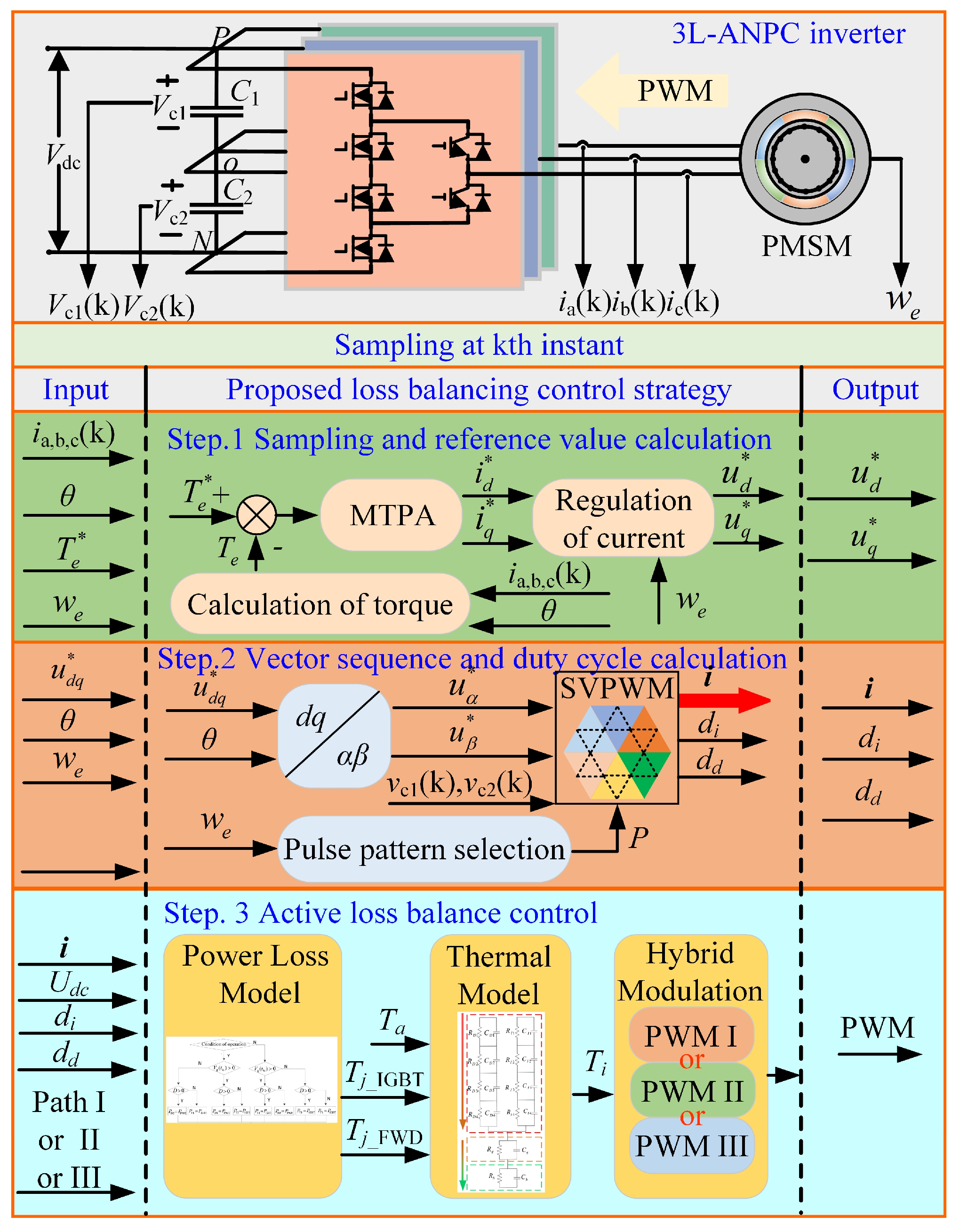
Figure 5 presents a block diagram illustrating the strategy for active thermal control of the permanent magnet synchronous traction system, incorporating junction temperature management and synchronous SVPWM for the 3L-ANPC inverter. Initially, the dq-axis reference current is derived from the reference torque calculation, and the dq-axis reference voltage is generated via the current regulator. Subsequently, the dq-axis reference voltage is transformed into the αβ-axis reference voltage. The synchronous SVPWM switching sequence and duty cycle are then determined by combining the dc-side capacitance voltage and pulse pattern. Finally, the junction temperature of the switching devices is calculated based on the commutation paths, coupled with the energy loss and temperature rise models. Using the hybrid modulation method described earlier, commutation paths I, II, and III are mixed according to the ratio specified in Equation (11). The selected high and low switching frequencies are applied, enabling closed-loop control of the device’s temperature rise.
4. Experimental Verification
To validate the effectiveness and feasibility of the proposed method, experiments were conducted on the traction inverter system within a Hardware-in-the-Loop (HIL) setup. The system parameters are provided in
Table 5. During the experiment, the bus voltage was set to 3000 V, the supporting capacitance to 0.002 F, the motor operated at 1000 rpm, and the applied torque was 3000 Nm.
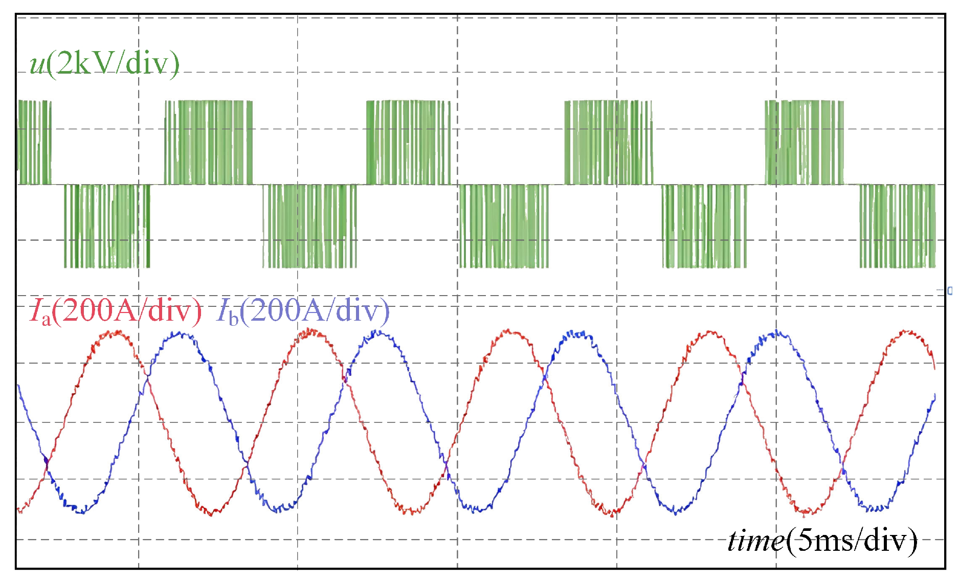
To assess the performance of the proposed algorithm, a hardware-in-the-loop control platform was established with a switching frequency of 1000 Hz. At operating conditions of 500 rpm and 3000 Nm, the output voltage and current waveforms were recorded, as shown in
Figure 6. Under these conditions, the output voltage was relatively low, and the line voltage exhibited a characteristic two-level waveform.
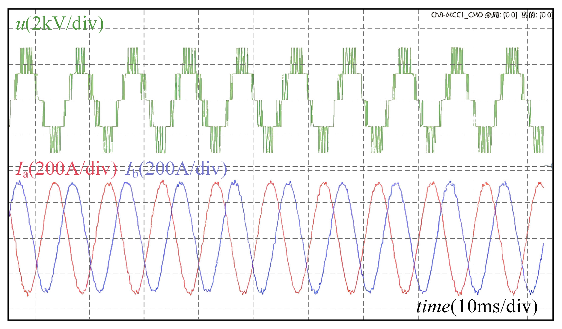
As the rotational speed increases, the output voltage transitions to a three-level waveform. The output line voltage and current waveforms at 2000 rpm are shown in
Figure 7. Due to the multi-level nature of the output voltage, the harmonics in the output current are significantly reduced.
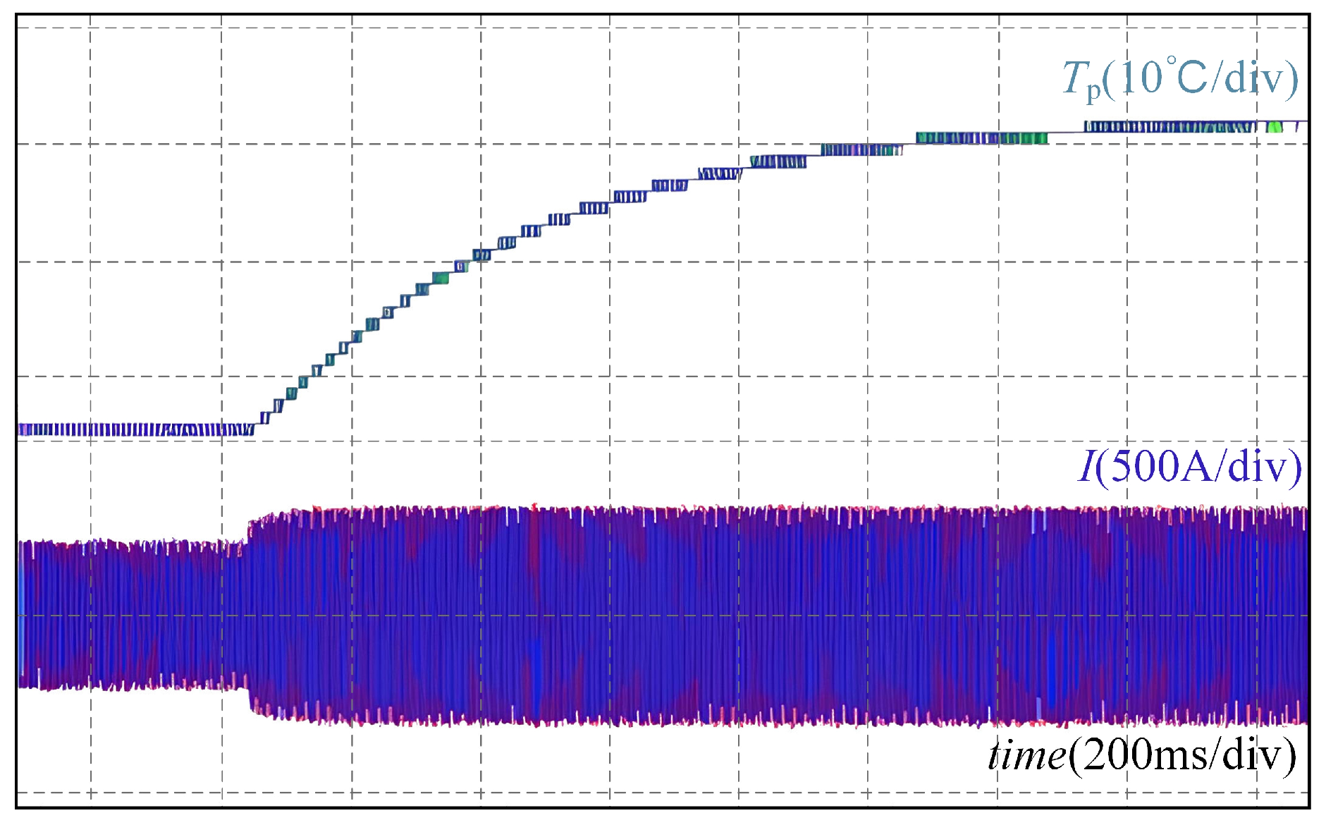
To validate the effectiveness of the closed-loop balance control for the ANPC loss and junction temperature estimation model, the simulated temperature rise in the two internal switches in the ANPC topology was compared under varying operating conditions.
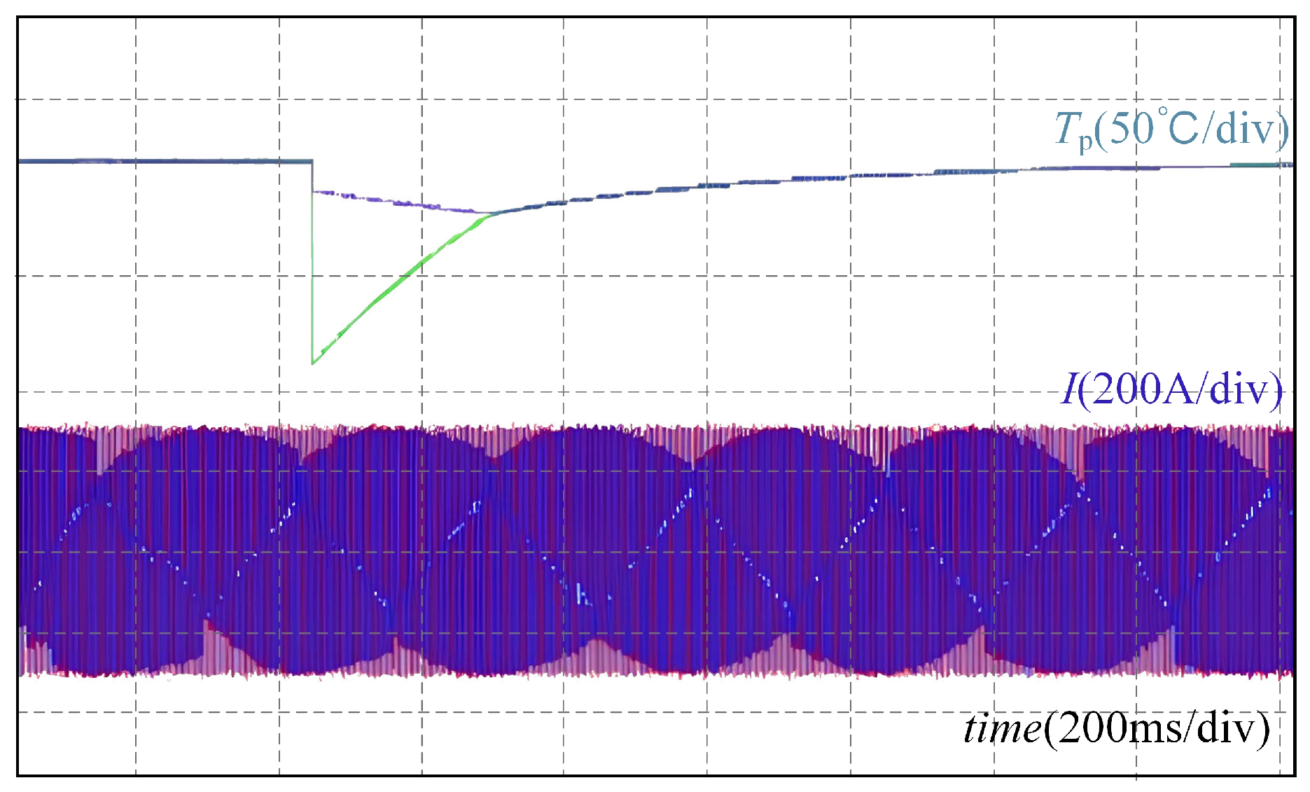
Figure 8 illustrates the temperature rise and current waveforms as the torque increases from 2000 Nm to 3000 Nm.
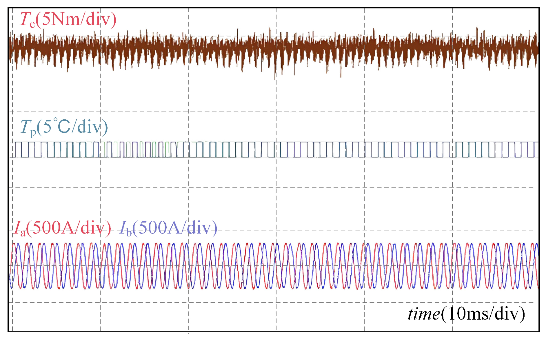
The waveforms of torque, temperature rise, and current under steady-state conditions are presented in
Figure 9.
A sudden change in the steady state leads to an abrupt variation in the initially estimated temperature rise in the internal switches, as depicted in the temperature rise and current waveforms in
Figure 10.
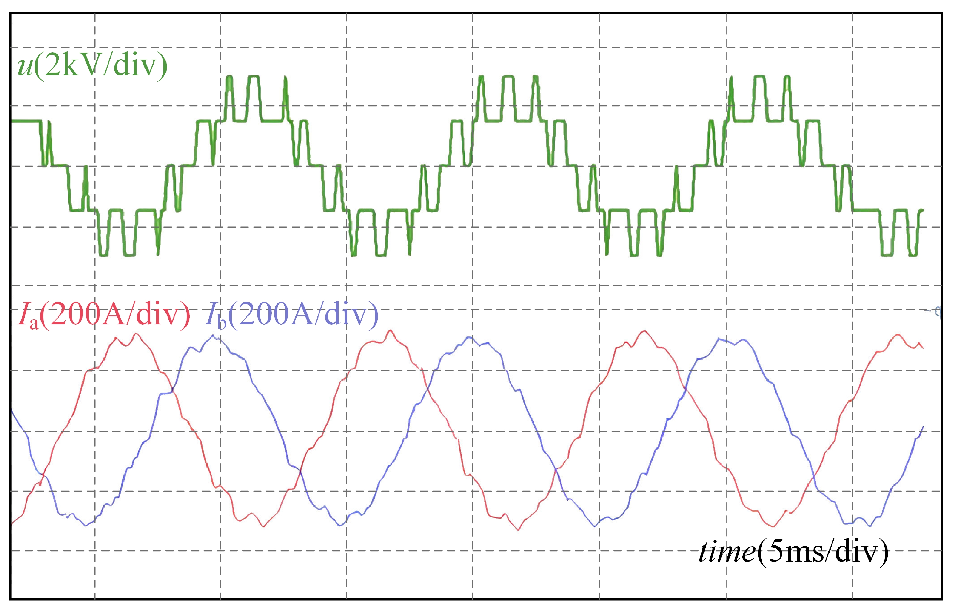
To further validate the ANPC synchronous modulation function, a Hardware-in-the-Loop experimental verification was performed. The corresponding voltage and current waveforms at 2000 rpm and 3000 Nm, with synchronization factor P = 3, are shown in
Figure 11.
The results from the Hardware-in-the-Loop experiments demonstrate that the proposed method, utilizing a loss-equalized closed-loop ANPC modulation strategy, effectively balances the temperature rise in the internal switches. Despite initial discrepancies in the temperature rise and during dynamic operation, the closed-loop modulation quickly equalizes the temperature. Additionally, through synchronous modulation, the output current harmonics are significantly reduced, ensuring that the traction system operates efficiently under a low switching frequency.
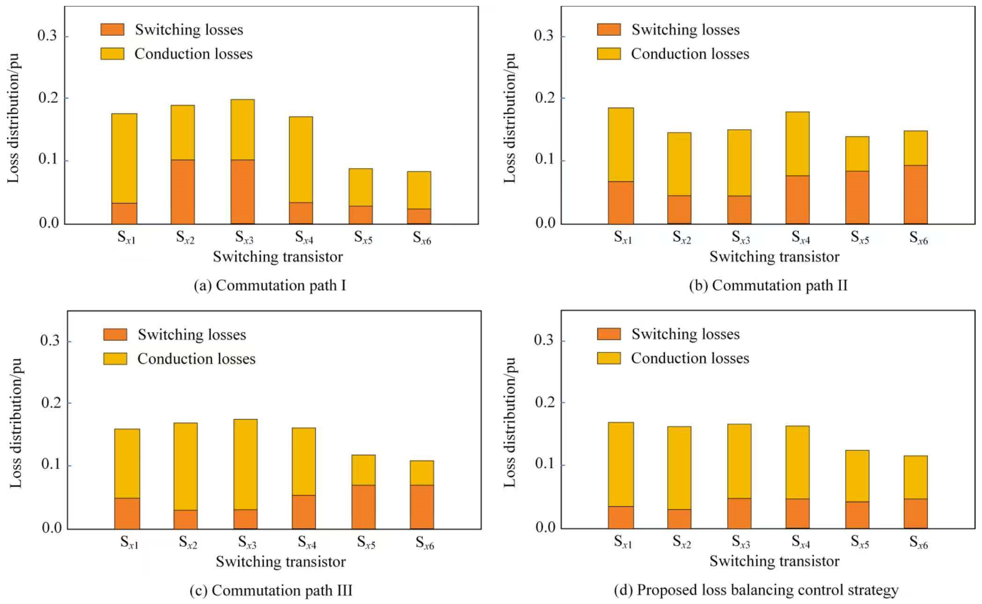
Figure 12 illustrates the loss distribution across each switching device in the ANPC single-phase bridge arm, controlled by commutation paths I, II, and III, as well as the proposed loss equalization strategy under identical operating conditions. The results clearly show that each modulation strategy has a distinct impact on the loss distribution.
At a constant current, the switching losses under the control of commutation path I are primarily concentrated in Sx2 and Sx3, whereas the losses under the control of commutation paths II and III are mainly concentrated in Sx1, Sx4, Sx5, and Sx6. Notably, the distribution of on-state losses and switching losses under the control of commutation paths II and III exhibit distinct characteristics. Importantly, the loss equalization control algorithm proposed in this study optimizes the distribution of both switching and conduction losses across each switching device in the ANPC inverter by mixing the three commutation paths. In summary, the proposed loss equalization strategy not only balances switching losses, but also ensures the equal distribution of conduction losses among the switches.
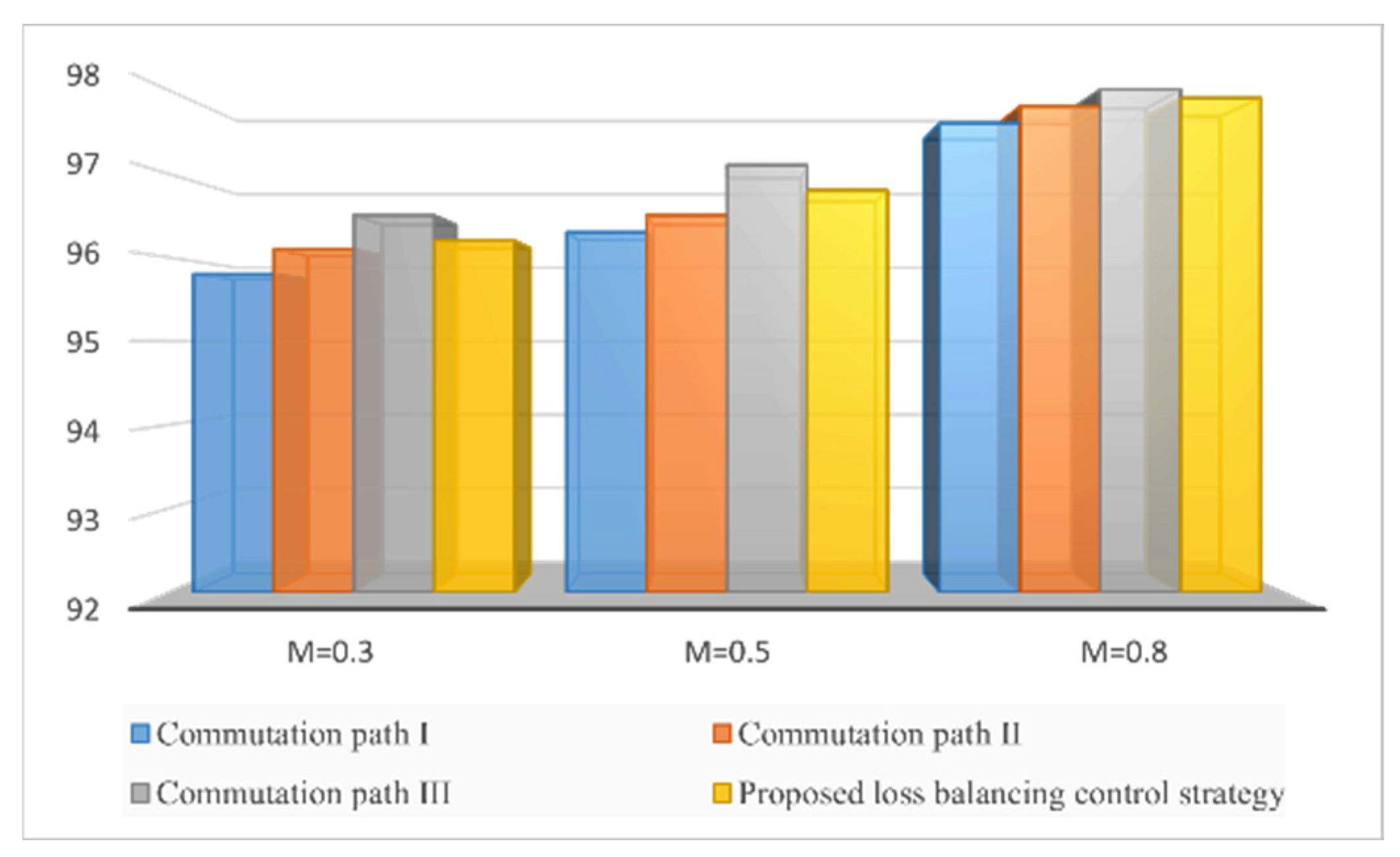
Figure 13 presents a comparison of efficiency for different modulation schemes, including commutation path I, commutation path II, commutation path III, and the proposed loss equalization strategy. The input power is calculated by multiplying the DC-bus voltage by the current, while efficiency is determined as the ratio of output power to input power. As the modulation regime increases from 0.3 to 0.8, the maximum efficiency for all four modulation methods improves. Under identical operating conditions, the highest efficiency is achieved using commutation path III, whereas commutation path I results in the lowest efficiency. The average operational efficiency of the proposed loss equalization strategy is slightly lower than that of commutation path III, which can be attributed to the need for the high-frequency pulse-width modulation to combine the three commutation paths (I, II, and III) effectively. This strategy not only balances switching and conduction losses, but also alleviates thermal stress on the ANPC inverter.
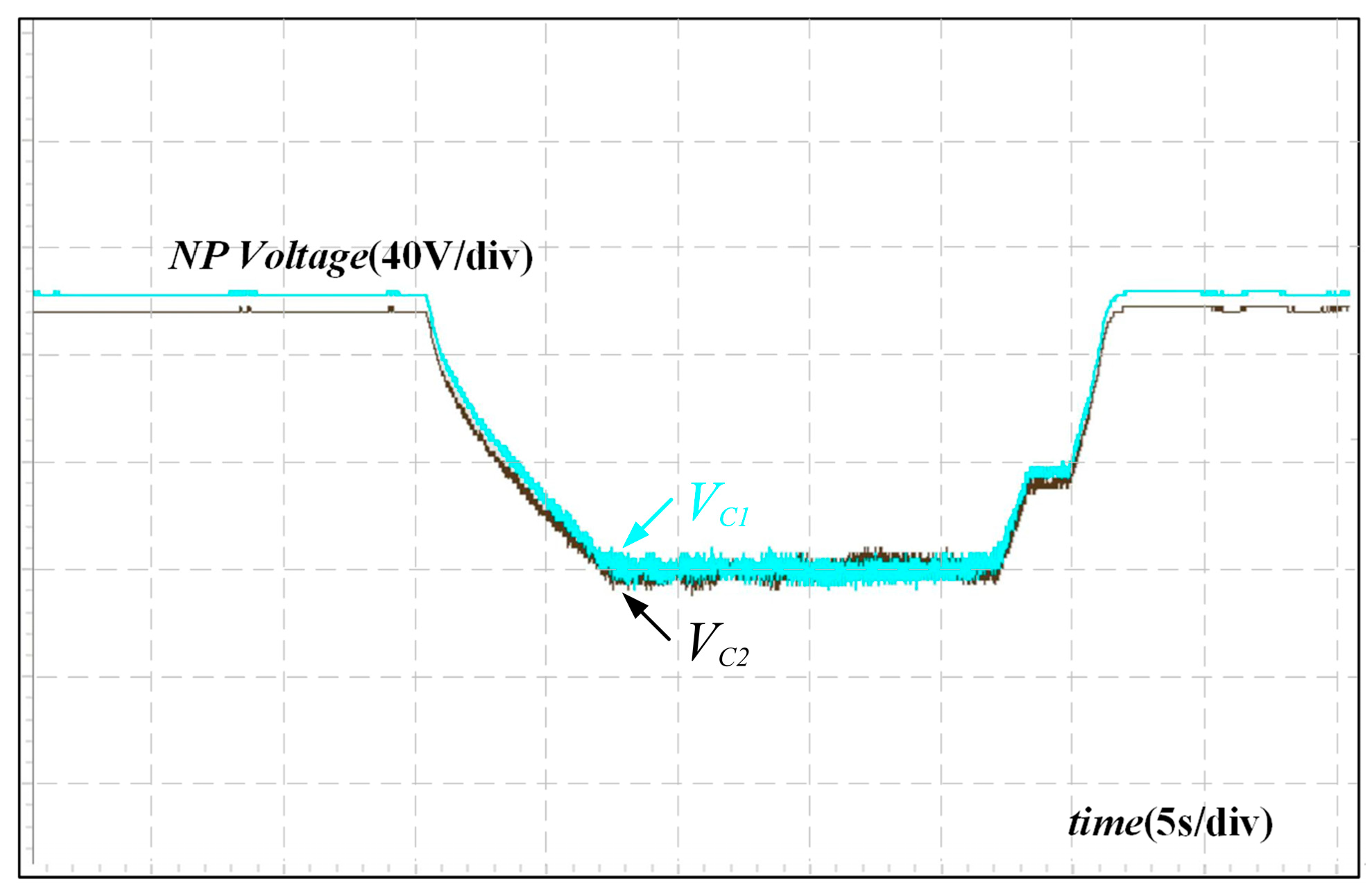
The dynamic experiments presented in
Figure 14 further validate the control performance of the proposed loss equalization strategy. To demonstrate the effectiveness of the NP voltage under the junction temperature closed-loop equalization control, the NP voltage difference is initially set to 40 V. When the NP balancing strategy is applied, the NP voltage (V) rapidly decreases from 40 V to near 0 V. This indicates that the introduction of junction temperature equalization constraints does not interfere with the balancing of the NP voltage. Furthermore, the NP voltage is quickly restored when any imbalance occurs on the DC side.


