


Zero–Average Dynamics Technique Applied to the Buck–Boost Converter: Results on Periodicity, Bifurcations, and Chaotic Behavior


Abstract
1. Introduction
- A detailed construction of the piecewise approximation of the switching surface.
- Existence of chaos is demonstrated numerically for positive Lyapunov exponents.
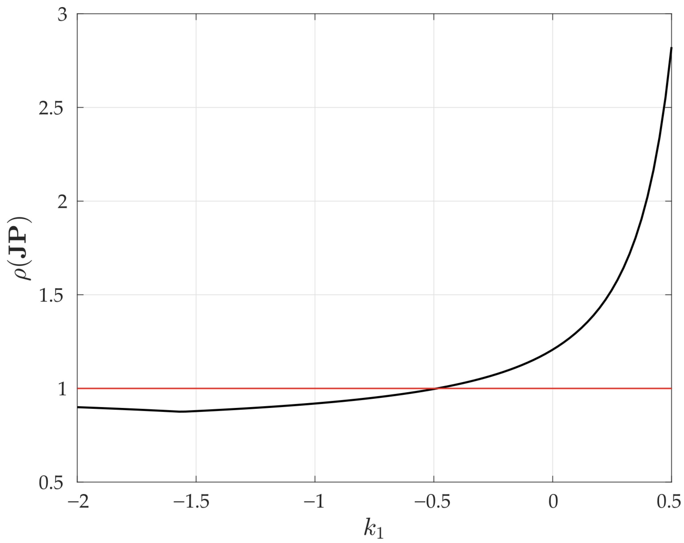
- Chaos in the Buck–Boost converter controlled with ZAD and FPIC is minimized, increasing the parameter of the FPIC.
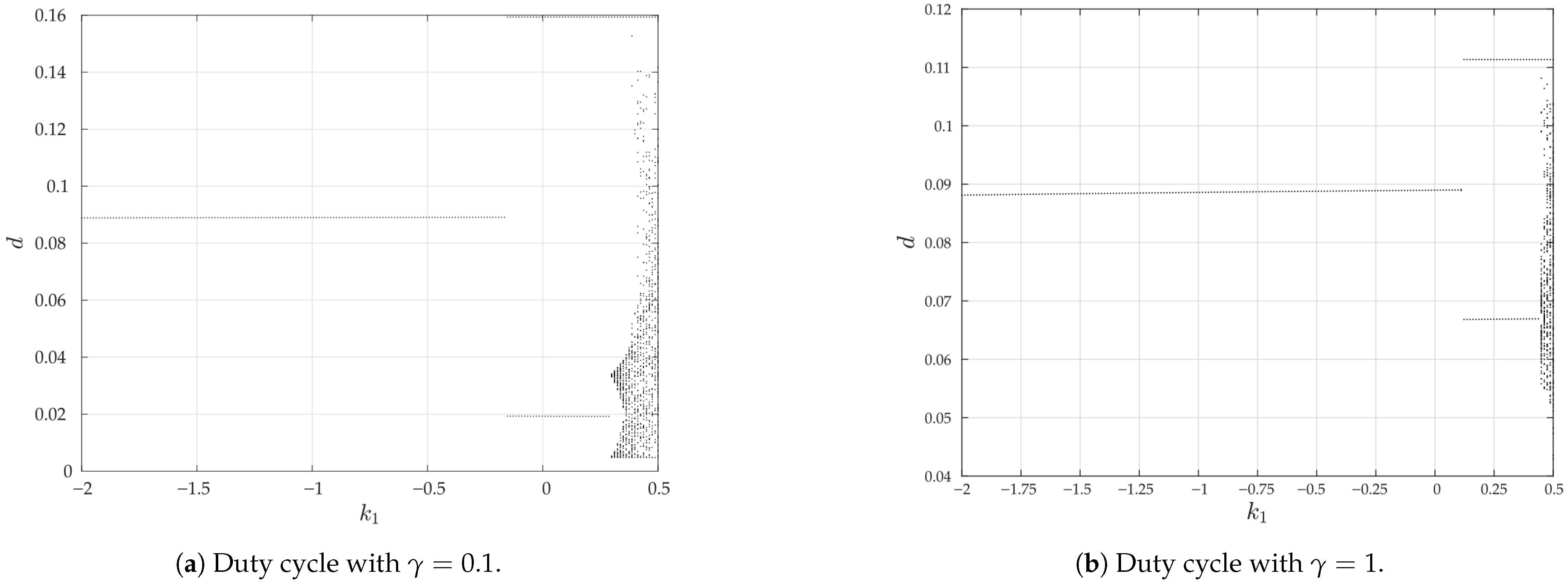
- Bifurcation diagrams are used to visualize the chaos is reduced when the value of is increased from to 1.
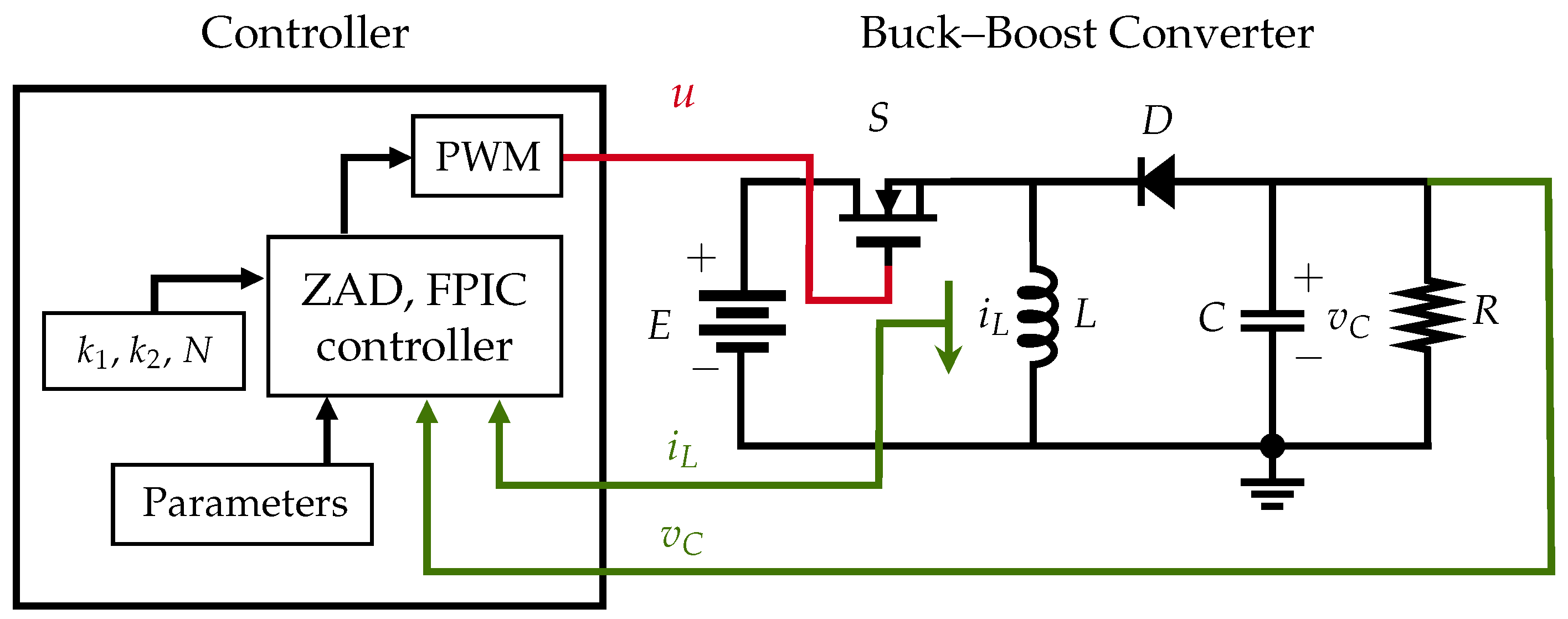
- The equations for a non-ideal Buck–Boost converter in continuous conduction mode (CCM) are presented, considering parasitic resistances of components and the mathematical model is experimentally validated, accounting for the effects of parasitic resistances. ZAD control is then applied to the model, including these parasitic effects, to effectively regulate the inductor current .
- A comparison of ZAD and PID control shows that both regulate current with less than 1% steady-state error.
- The ZAD control maintains a balanced duty cycle without saturation, avoiding chattering, while the PID control exhibits saturation in the duty cycles, which can cause stability issues.
- This study presents the first application of ZAD control to a Buck–Boost converter with parasitic resistances, creating a more realistic model. Unlike previous works on Boost converters, this approach addresses the non-minimum phase behavior and stability challenges of Buck–Boost converters, enhancing control reliability.
2. Materials and Methods
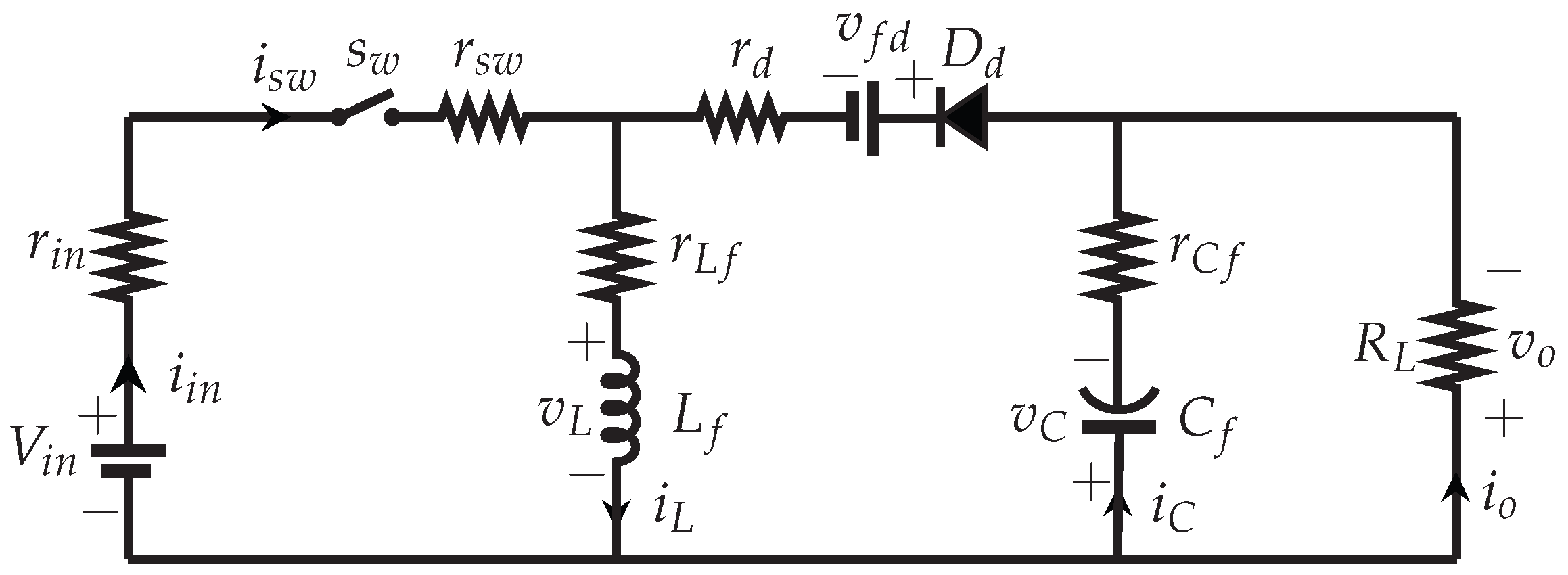
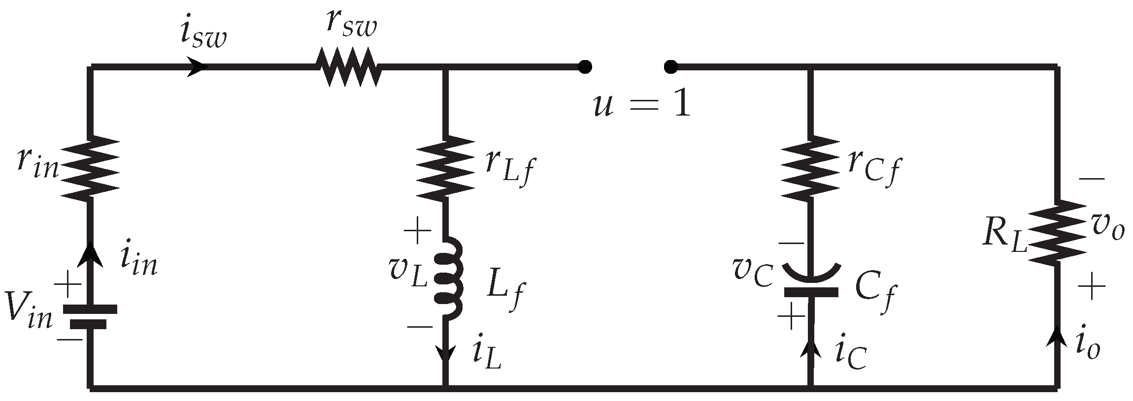
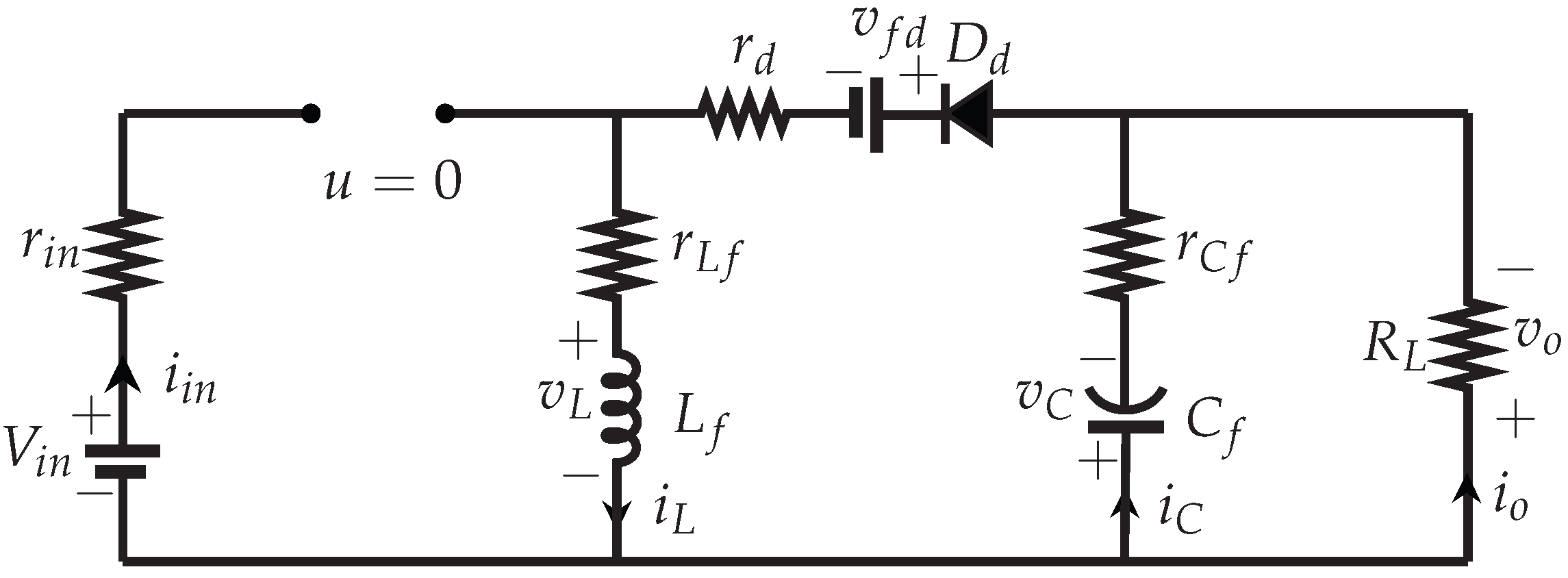
2.1. Buck–Boost Converter
2.2. Dimensionless System
2.3. Switching Surface
- is the state vector, with as the voltage state and as the current state,
- is the reference vector, whose components are the voltage and current reference signals. This vector corresponds to the state to which we want the system to evolve.
- is the parameter vector of the switching surface, which contains the constant components and associated with the error between the output signal and the reference signal.
- The difference represents the error in voltage and current, respectively.
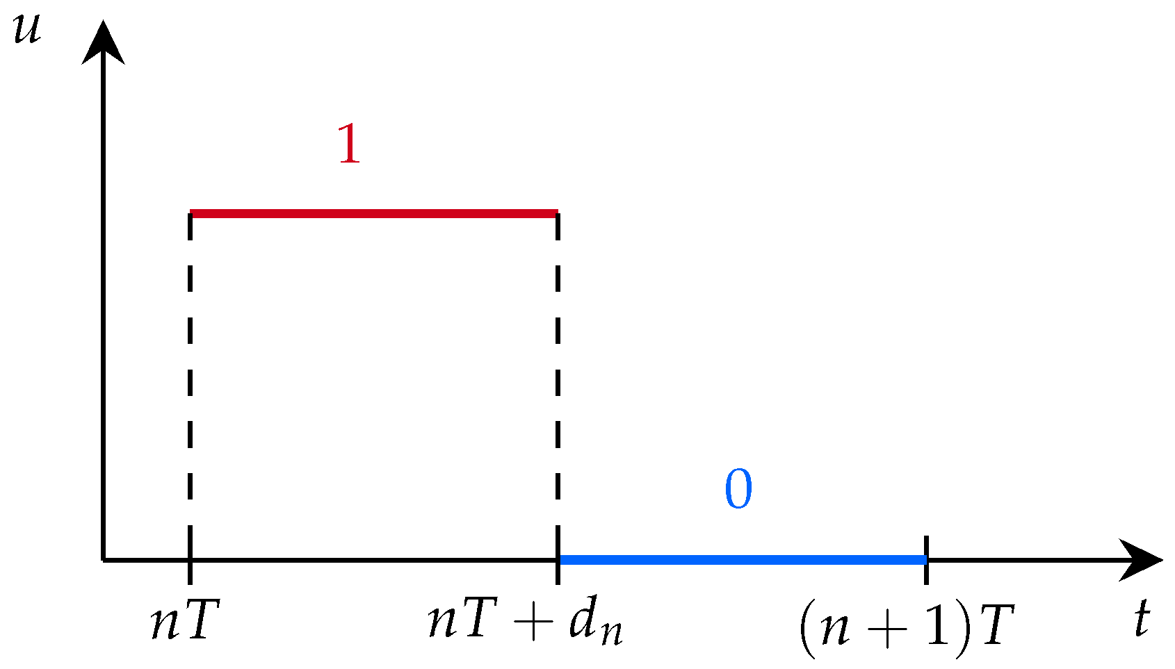
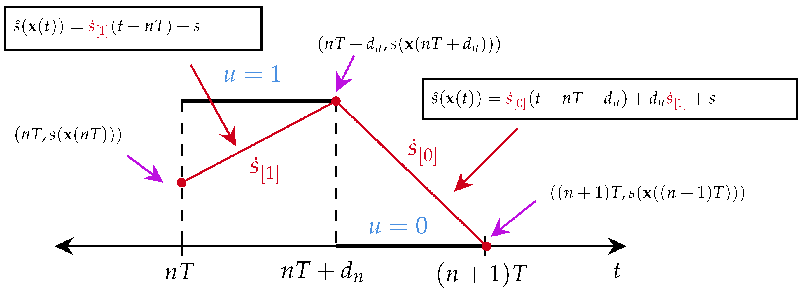
2.4. Duty Cycle
- (i)
- The dynamics of the error or switching surface behave as piecewise linear segments.
- (ii)
- The slopes of the error dynamics in the intervals and are determined by and , calculated at the moment of switching. Both slopes correspond to the time derivative of the switching surface for and , respectively, evaluated at .
- Topology . Suppose , then takes complex values. To resolve this issue, is chosen as the value minimizing [19]. By differentiation, the minimum of this polynomial is attained at . Therefore, is chosen as .
- Topologies and . Suppose , then , implying . Thus, it follows that . When , we say the duty cycle is unsaturated.
- Topology . Suppose , then , and therefore . Since is strictly greater than zero, we choose .
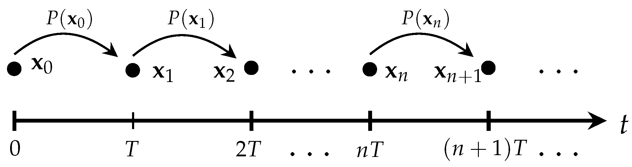
2.5. Poincaré Map
2.6. Stability of Periodic Orbits
- For , we have
- And for , we have
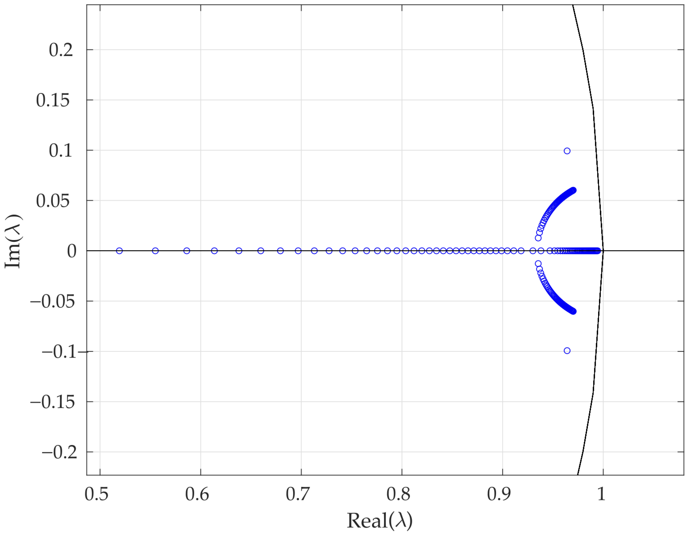
2.7. Chaos Existence in the Buck–Boost Converter
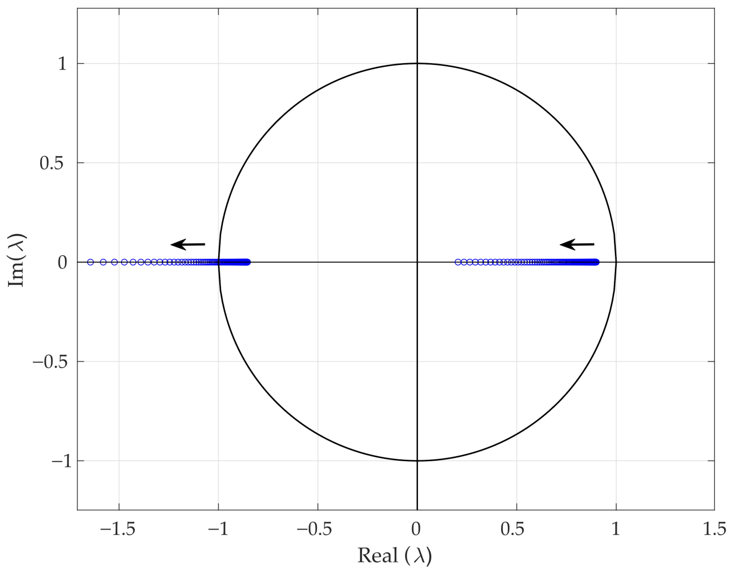
2.8. Chaos Control with FPIC
2.9. Model with Parasitic Resistors
3. Results
3.1. Performance of the ZAD Strategy


3.2. Bifurcations in the Buck–Boost Converter
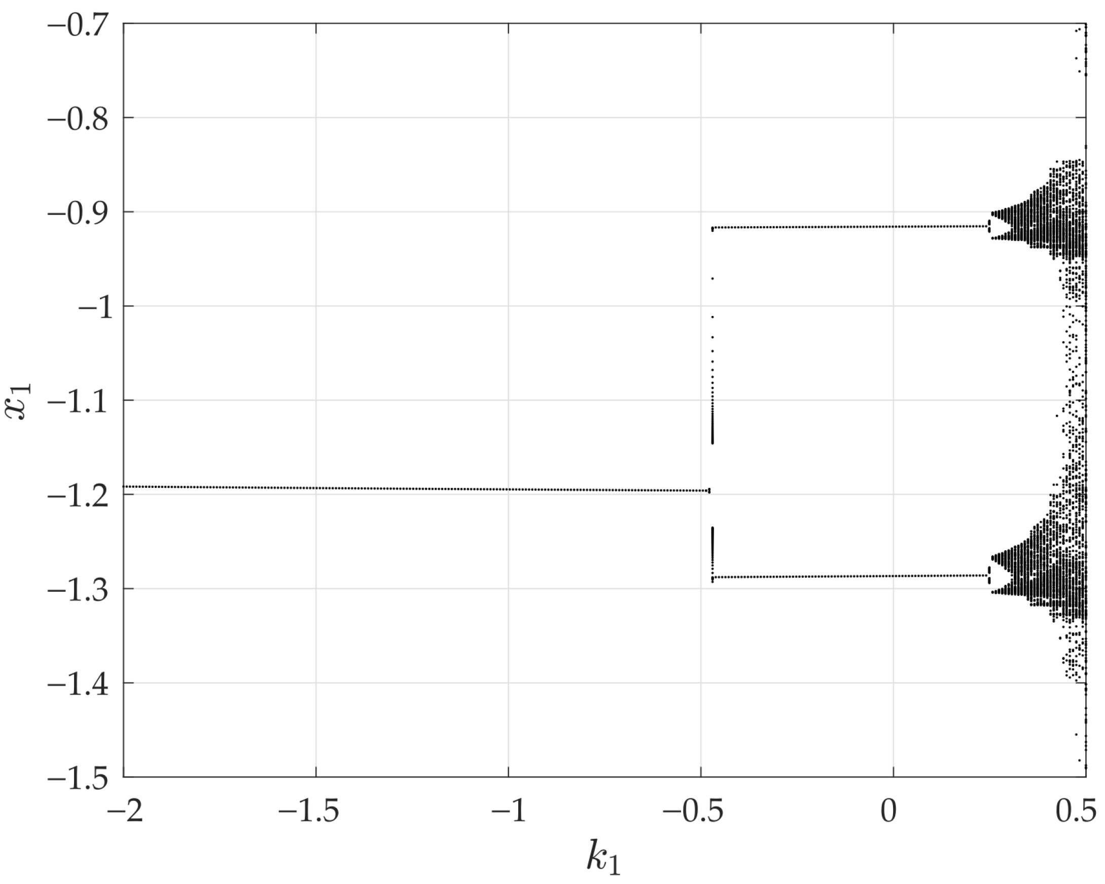
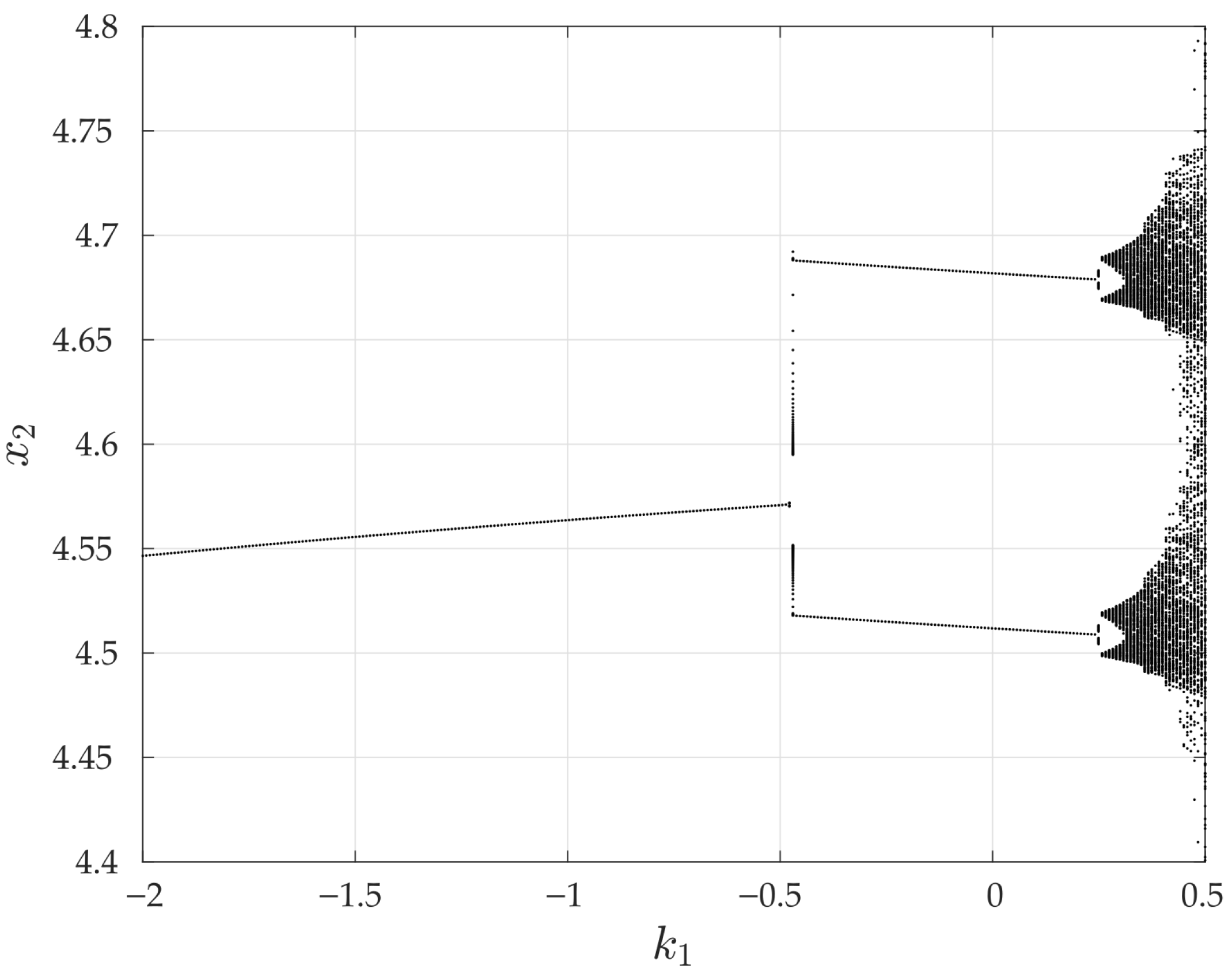
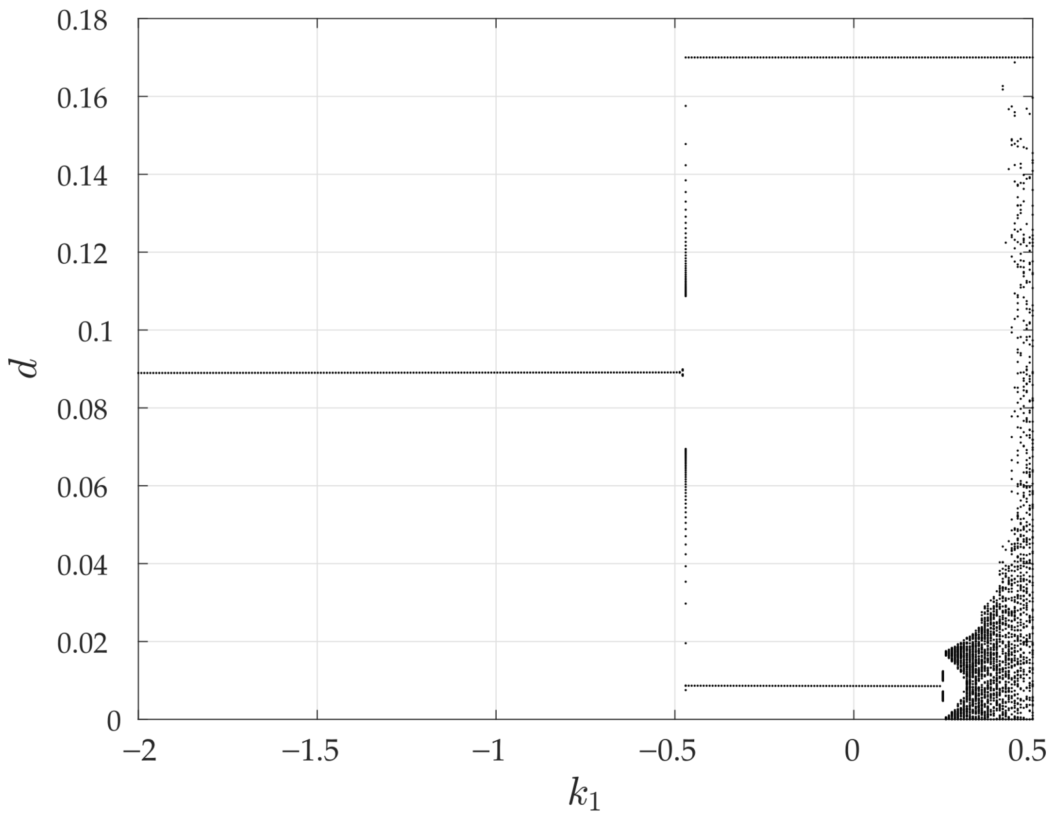
3.3. Existence and Stability of -Periodic Orbits
- (i)
- The initial condition was kept fixed, equal to or close to the reference values.
- (ii)
- The parameter vector of the switching surface was fixed.
- (iii)
- The system parameter Q was varied over an appropriate range of values.

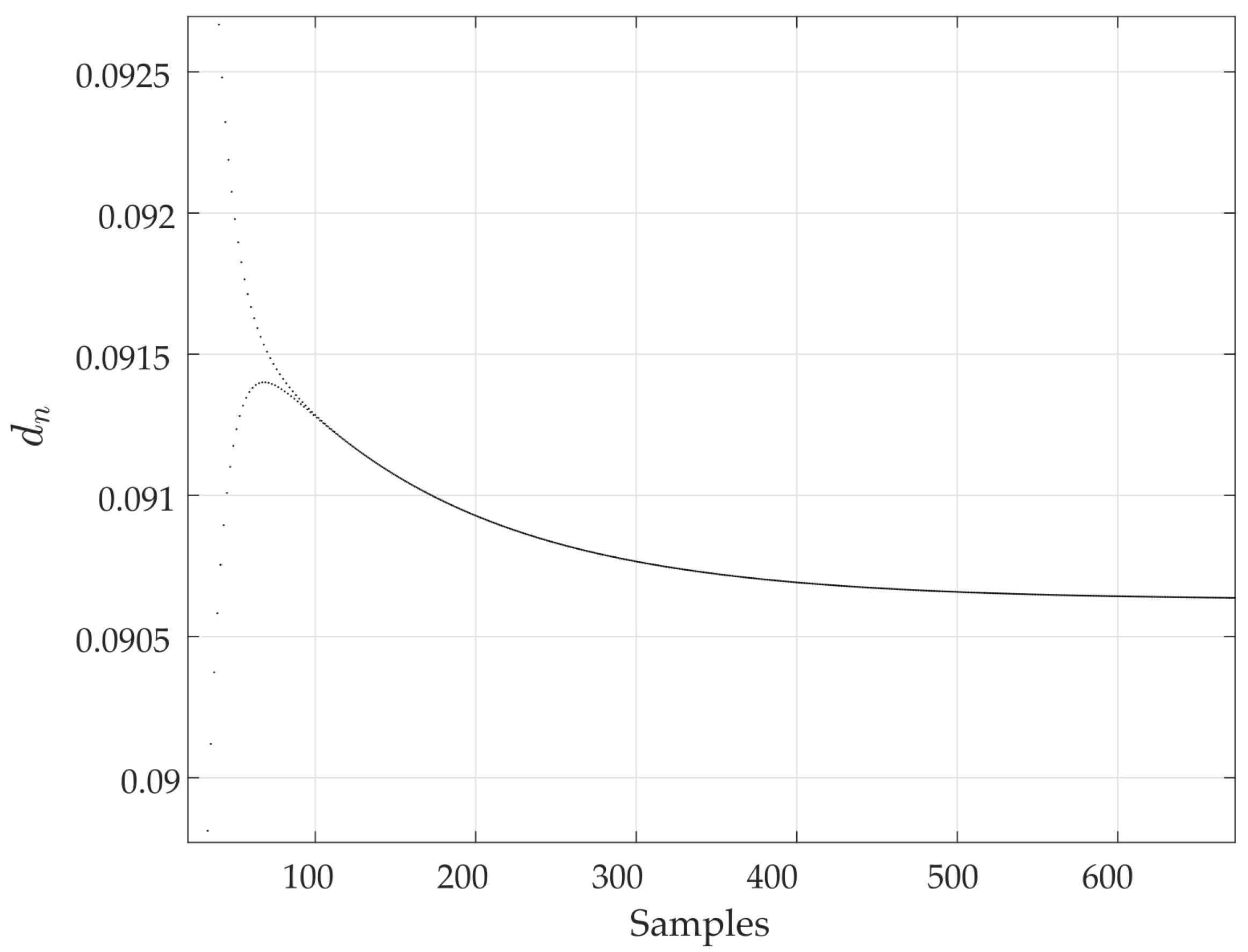
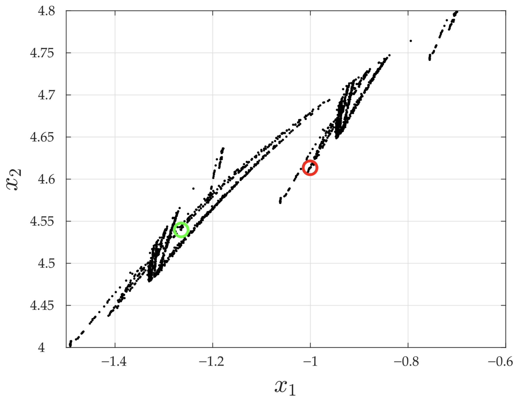
3.4. Chaos in the Buck–Boost Converter
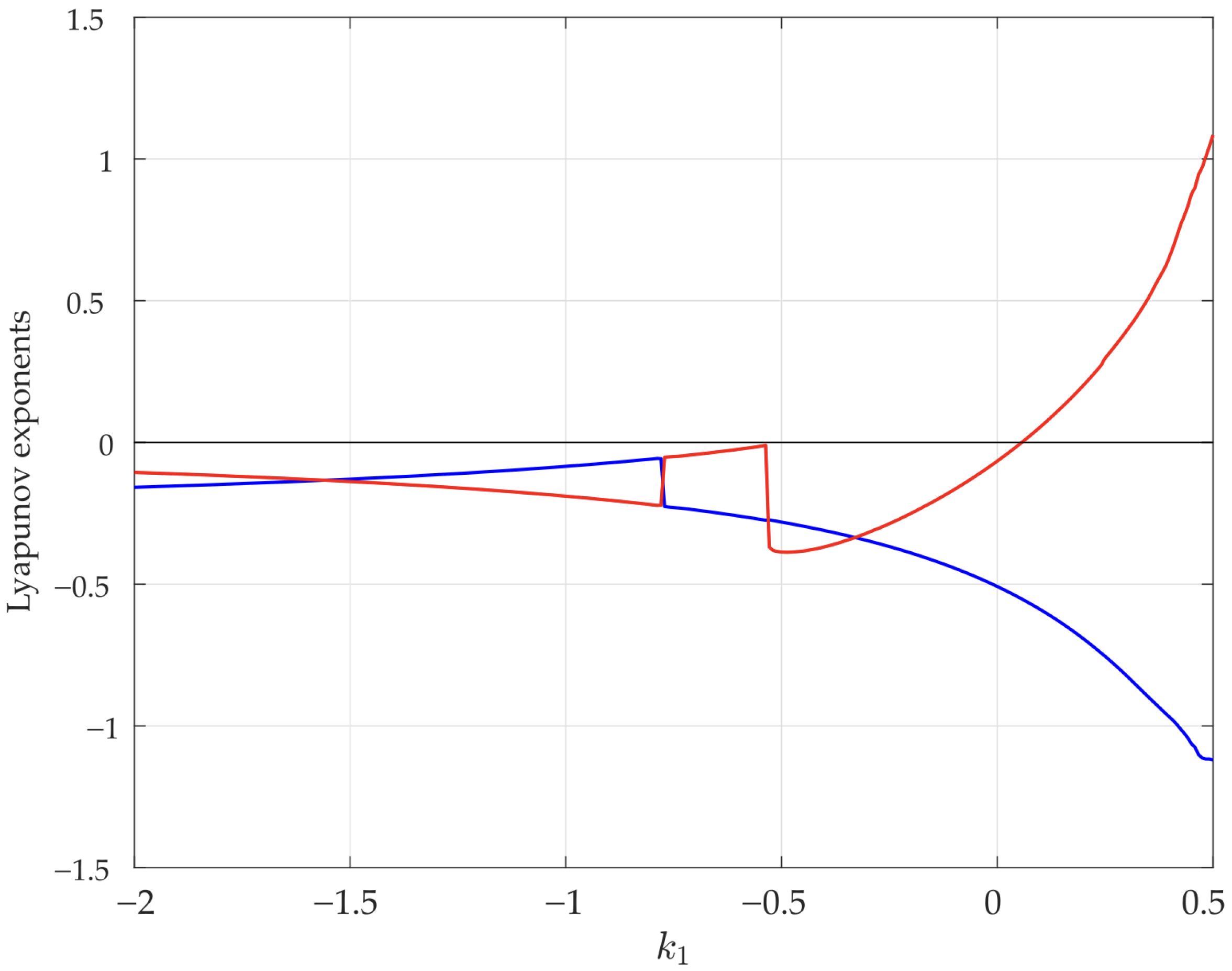
3.5. Instabilities Control with FPIC


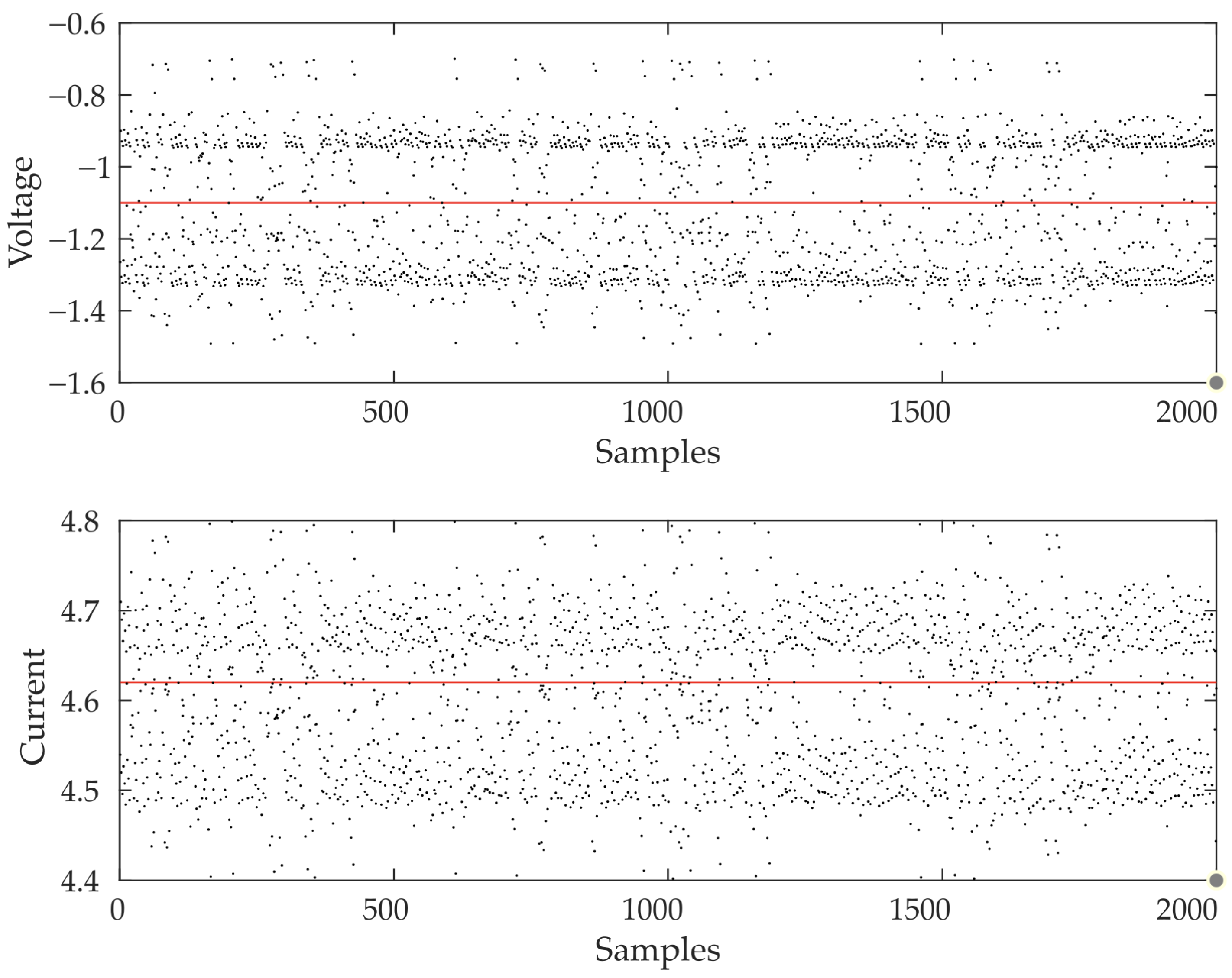
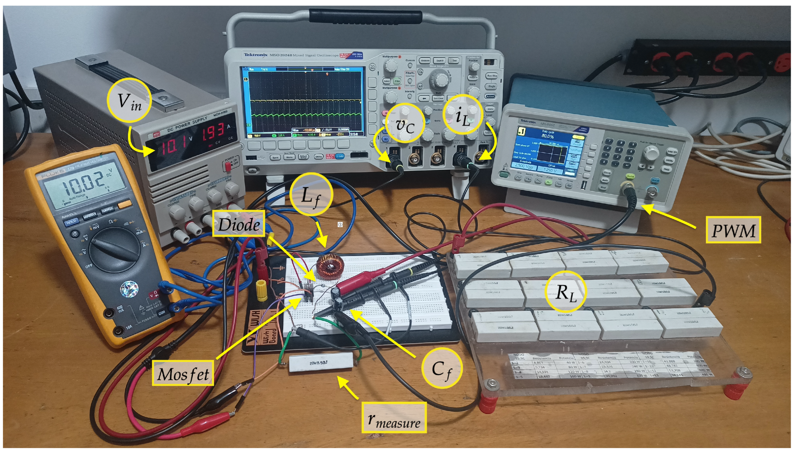
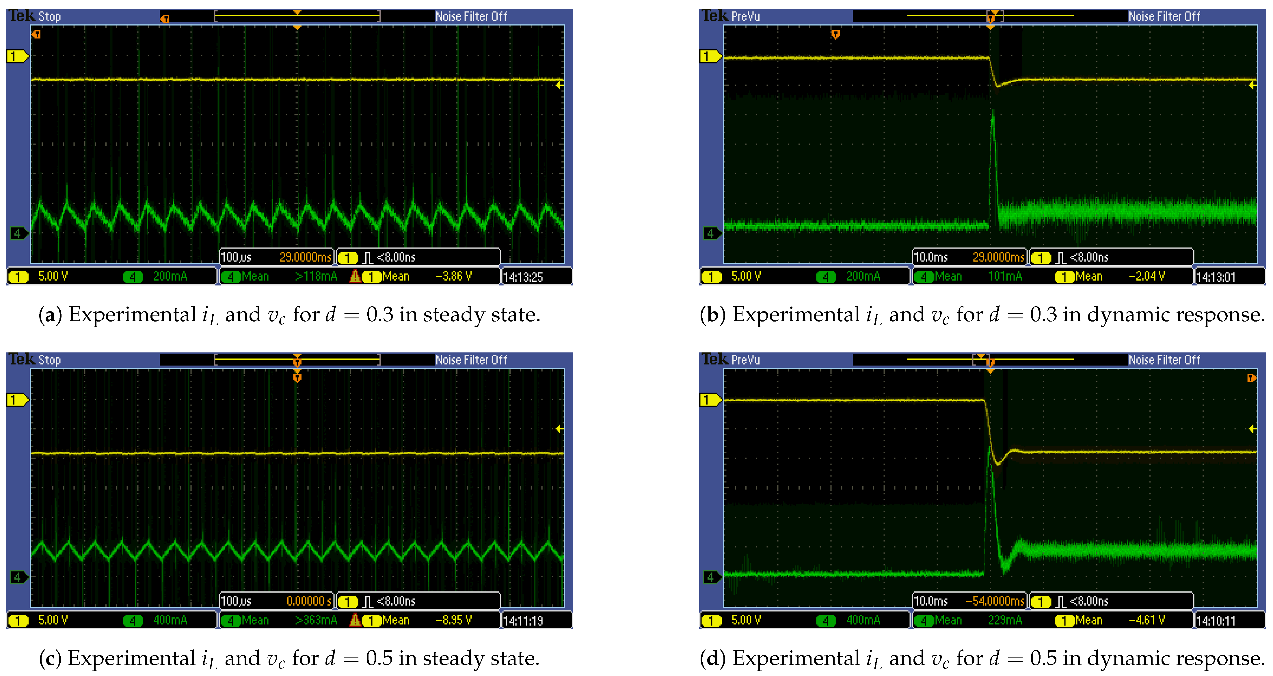
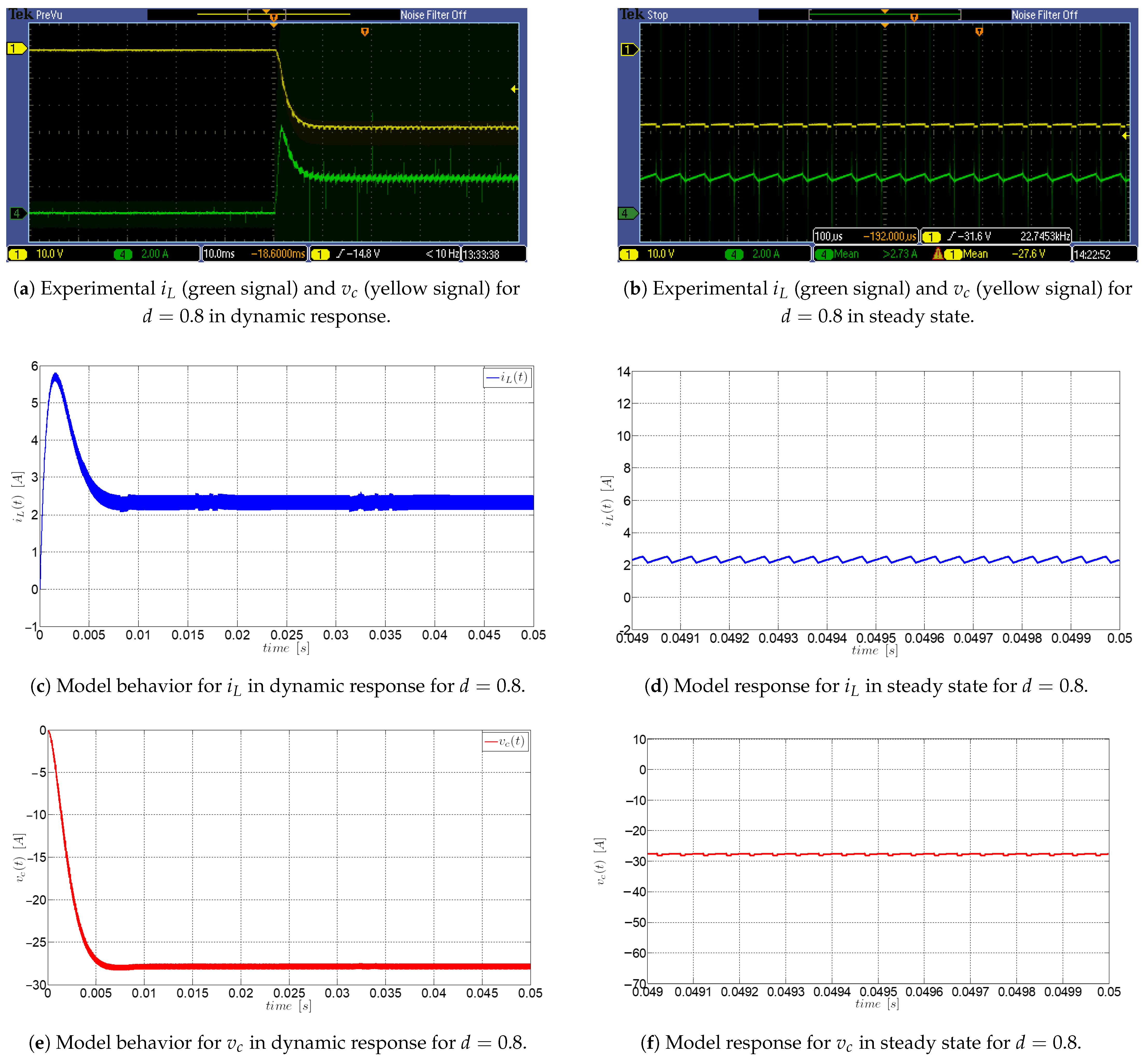
3.6. Validation of the Buck–Boost Converter Model with Parasitic Resistances: Experimental and Numerical Analysis
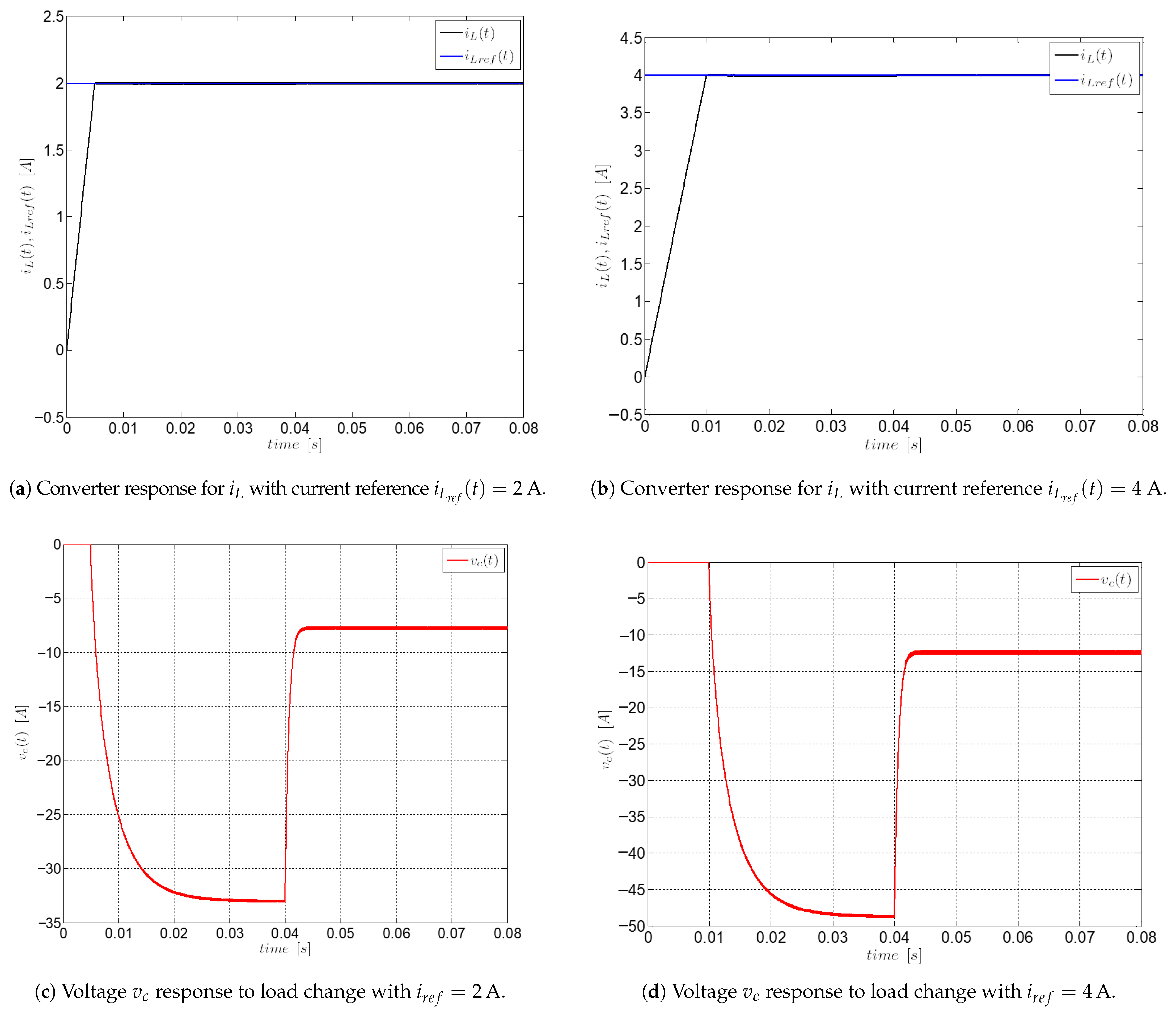
3.7. Closed-Loop Current Control of a Buck–Boost Converter Using the ZAD Technique
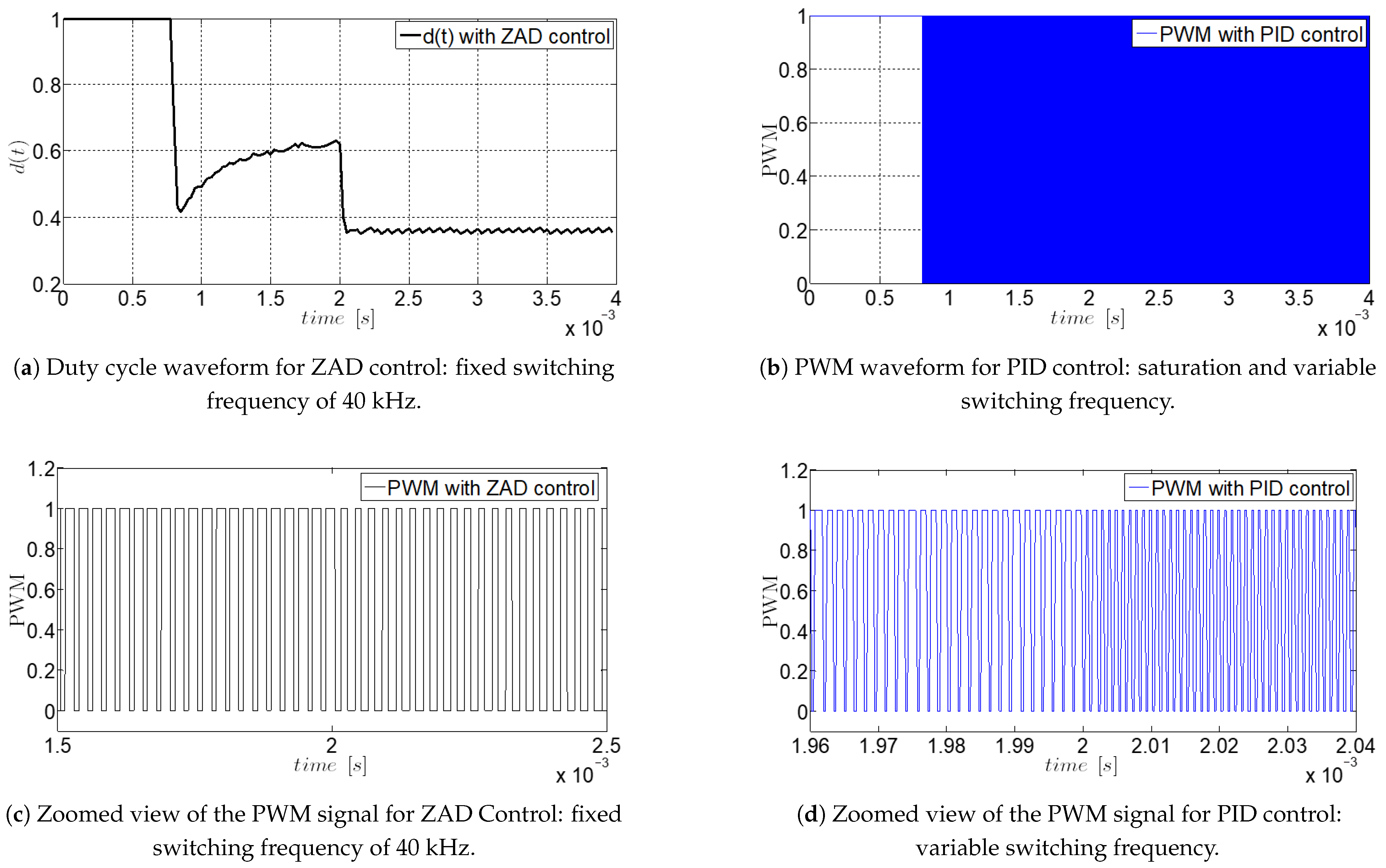
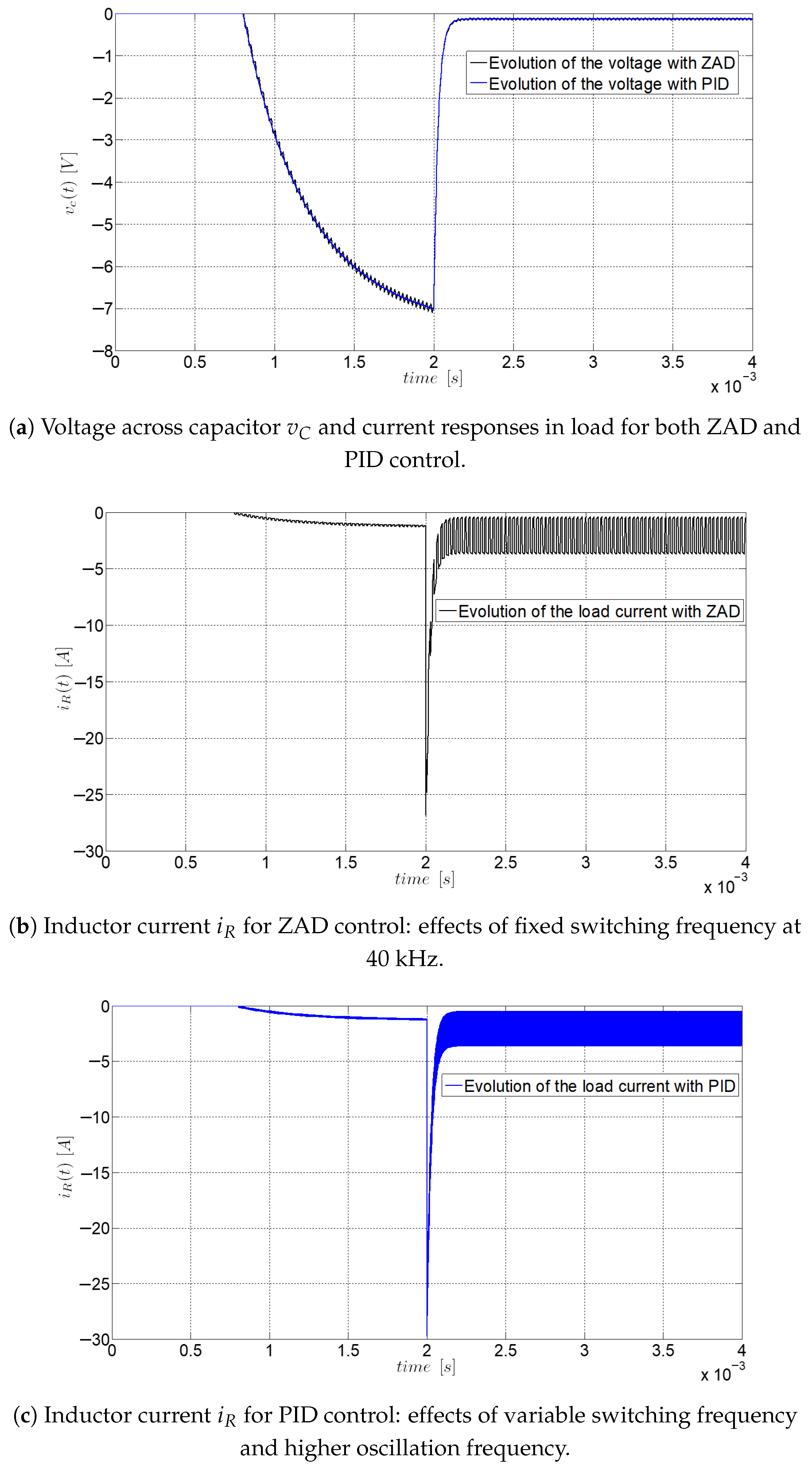
3.8. Comparison of ZAD and PID Control for Buck–Boost System
4. Conclusions
Author Contributions
Funding
Data Availability Statement
Acknowledgments
Conflicts of Interest
Abbreviations
| ZAD | Zero Average Dynamics |
| FPIC | Fixed Point Induced Control |
| PID | Proportional-Integral-Derivative |
| PWM | Pulse Width Modulation |
| MOSFET | Metal-Oxide-Semiconductor Field-Effect Transistor |
| LPWM | Left Pulse-Width Modulation |
| CPWM | Centered Pulse-Width Modulation |
References
- Casanova Trujillo, S.; Candelo-Becerra, J.E.; Hoyos, F.E. Analysis and Control of Chaos in the Boost Converter with ZAD, FPIC, and TDAS. Sustainability 2022, 14, 13170. [Google Scholar] [CrossRef]
- Narasimha, S.; Salkuti, S.R. Design and operation of closed-loop triple-deck Buck–Boost converter with high gain soft switching. Int. J. Power Electron. Drive Syst. (IJPEDS) 2020, 11, 523–529. [Google Scholar] [CrossRef]
- Kurniawan, F.; Lasmadi, L.; Dinaryanto, O.; Sudibya, B.; Nasution, M.R.E. A novel Boost-Buck converter architecture for improving transient response and output-voltage ripple. J. Ict Res. Appl. 2020, 14, 149. [Google Scholar] [CrossRef]
- Mutta, C.; Goswami, A.D. Design of an efficient convolutional Buck–Boost converter for hybrid bioinspired parameter tuning. Bull. Electr. Eng. Inform. 2023, 12, 2705–2716. [Google Scholar] [CrossRef]
- Abdelsalam, I.; Adam, G.P.; Holliday, D.; Williams, B. Single-stage, single-phase, ac–dc Buck–Boost converter for low-voltage applications. IET Power Electron. 2014, 7, 2496–2505. [Google Scholar] [CrossRef]
- Trujillo, S.C.; Candelo-Becerra, J.E.; Hoyos, F.E. Performance of the Boost converter controlled with zad to regulate dc signals. Computation 2021, 9, 96. [Google Scholar] [CrossRef]
- He, L.; Jia, M.; Sun, G. Chaos control for the Buck–Boost converter under current-mode control. In Proceedings of the Third International Workshop on Advanced Computational Intelligence, Suzhou, China, 25–27 August 2010. [Google Scholar] [CrossRef]
- Cheng, K.W.E.; Liu, M.; Wu, J.; Cheung, N.C. Study of bifurcation and chaos in the current-mode controlled Buck–Boost DC–DC converter. In Proceedings of the IECON’01—27th Annual Conference of the IEEE Industrial Electronics Society, Denver, CO, USA, 29 November–2 December 2001. [Google Scholar] [CrossRef]
- Guo, Y.L.; Wang, L.; Wu, Q.H. Bifurcation Control Method for Buck–Boost Converters Based on Energy Balance Principle. IEEE J. Emerg. Sel. Top. Power Electron. 2021, 9, 1250245. [Google Scholar] [CrossRef]
- Palanidoss, S.; Kavitha, A.; Padmanaban, S.; Ramachandaramurthy, V.K. Control of chaos in a current mode controlled Buck–Boost converter using weak periodic perturbation method. Int. J. Power Electron. Drive Syst. (IJPEDS) 2015, 8, 1467–1480. [Google Scholar] [CrossRef]
- Natsheh, A.N.; Kettleborough, J.G. Control of chaotic behaviour in Buck–Boost DC–DC converters. In Proceedings of the 2012 24th International Conference on Microelectronics (ICM), Algiers, Algeria, 16–20 December 2012. [Google Scholar] [CrossRef]
- Hoyos, F.E.; Burbano, D.; Angulo, F.; Olivar, G.; Toro, N.; Taborda, J.A. Effects of quantization, delay, and internal resistances in digitally ZAD-controlled Buck converter. Int. J. Bifurc. Chaos 2012, 22, 1250245. [Google Scholar] [CrossRef]
- Hoyos Velasco, F.E.; García, N.T.; Garcés Gómez, Y.A. Adaptive control for Buck power converter using fixed point inducting control and zero average dynamics strategies. Int. J. Bifurc. Chaos 2015, 25, 1550049. [Google Scholar] [CrossRef]
- Hoyos, F.E.; Candelo-Becerra, J.E.; Toro, Y. Numerical and experimental validation with bifurcation diagrams for a controlled DC–DC converter with quasi-sliding control. TecnoLógicas 2018, 21, 147–167. [Google Scholar] [CrossRef]
- Hoyos, F.E.; Candelo-Becerra, J.E.; Hoyos Velasco, C.I. Model-based quasi-sliding mode control with loss estimation applied to DC–DC power converters. Electronics 2019, 8, 1086. [Google Scholar] [CrossRef]
- Muñoz, J.-G.; Angulo, F.; Angulo-Garcia, D. Zero average surface controlled Boost-flyback converter. Energies 2021, 14, 57. [Google Scholar] [CrossRef]
- Hoyos, F.E.; Candelo-Becerra, J.E.; Hoyos Velasco, C.I. Application of zero average dynamics and fixed point induction control techniques to control the speed of a DC motor with a Buck converter. Appl. Sci. 2020, 10, 1807. [Google Scholar] [CrossRef]
- Angulo, F.; Olivar, G.; di Bernardo, M. Two-parameter discontinuity-induced bifurcation curves in a ZAD-strategy-controlled dc-dc Buck converter. IEEE Trans. Circuits Syst. I Regul. Pap. 2008, 55, 2392–2401. [Google Scholar] [CrossRef]
- Amador, A.; Casanova, S.; Granada, H.A.; Olivar, G.; Hurtado, J. Codimension-Two Big-Bang Bifurcation in a ZAD-Controlled Boost DC–DC Converter. Int. J. Bifurc. Chaos 2014, 24, 1450150. [Google Scholar] [CrossRef]
- Toro García, N.; Garcés Gomez, Y.A.; Henao Cespedes, V. Robust control technique in power converter with linear induction motor. Int. J. Power Electron. Drive Syst. 2022, 13, 340–347. [Google Scholar] [CrossRef]
- Deivasundari, P.; Uma, G.; Simon, A. Chaotic dynamics of a zero average dynamics controlled DC–DC Ćuk converter. IET Power Electron. 2014, 7, 289–298. [Google Scholar] [CrossRef]
- Fossas, E.; Griñó, R.; Biel, D. Quasi-sliding control based on pulse width modulation, Zero averaged dynamics and the L2 norm. In Advances in Variable Structure Systems: Analysis, Integration and Applications; World Scientific Publishing Co. Pte. Ltd.: Singapore, 2000; pp. 335–344. [Google Scholar] [CrossRef]
- Fossas, E.; Olivar, G. Study of chaos in the Buck converter. IEEE Trans. Circuits Syst. I Fundam. Theory Appl. 1996, 43, 13–25. [Google Scholar] [CrossRef]
- Toribio, E.; El Aroudi, A.; Olivar, G.; Benadero, L. Numerical and experimental study of the region of period-one operation of a PWM Boost converter. IEEE Trans. Power Electron. 2000, 15, 1163–1171. [Google Scholar] [CrossRef]
- Poddar, G.; Chakrabarty, K.; Banerjee, S. Experimental control of chaotic behavior of Buck converter. IEEE Trans. Circuits Syst. I Fundam. Theory Appl. 1995, 42, 502–504. [Google Scholar] [CrossRef]
- Di Bernardo, M.; Garefalo, F.; Glielmo, L.; Vasca, F. Switchings, bifurcations, and chaos in DC/DC converters. IEEE Trans. Circuits Syst. I Fundam. Theory Appl. 1998, 45, 133–141. [Google Scholar] [CrossRef]
- Munoz, J.; Osorio, G.; Angulo, F. Boost converter control with ZAD for power factor correction based on FPGA. In Proceedings of the 2013 Workshop on Power Electronics and Power Quality Applications (PEPQA), Bogota, Colombia, 6–7 July 2013; pp. 1–5. [Google Scholar] [CrossRef]
- Angulo, F.; Burgos, J.; Olivar, G. Chaos stabilization with TDAS and FPIC in a Buck converter controlled by lateral PWM and ZAD. In Proceedings of the 2007 Mediterranean Conference on Control & Automation, Athens, Greece, 27–29 June 2007; pp. 1–6. [Google Scholar] [CrossRef]
- Aroudi, A.E.; Debbat, M.; Martinez-Salamero, L. Poincaré maps modeling and local orbital stability analysis of discontinuous piecewise affine periodically driven systems. Nonlinear Dyn. 2007, 50, 431–445. [Google Scholar] [CrossRef]
- Repecho, V.; Biel, D.; Ramos-Lara, R. Robust ZAD Sliding Mode Control for an 8-Phase Step-Down Converter. IEEE Trans. Power Electron. 2020, 35, 2222–2232. [Google Scholar] [CrossRef]
- Vergara Perez, D.D.C.; Trujillo, S.C.; Hoyos Velasco, F.E. Period Addition Phenomenon and Chaos Control in a ZAD Controlled Boost Converter. Int. J. Bifurc. Chaos 2018, 28, 1850157. [Google Scholar] [CrossRef]
- Repecho, V.; Biel, D.; Ramos-Lara, R.; Vega, P.G. Fixed-Switching Frequency Interleaved Sliding Mode Eight-Phase Synchronous Buck Converter. IEEE Trans. Power Electron. 2018, 33, 676–688. [Google Scholar] [CrossRef]
- Ullah, Q.; Wu, X.; Saleem, U. Current Controlled Robust Four-Switch Buck–Boost DC–DC Converter. In Proceedings of the 2021 International Conference on Computing, Electronic and Electrical Engineering (ICE Cube), Multan, Pakistan, 11–12 March 2021; pp. 1–6. [Google Scholar] [CrossRef]
- Sira Ramírez, J.; Silva-Ortigoza, R. Control Design Techniques in Power Electronics Devices; Springer: London, UK, 2006. [Google Scholar]
- Hoyos Velasco, F.E.; Candelo, J.E.; Silva Ortega, J.I. Performance evaluation of a DC-AC inverter controlled with ZAD-FPIC. Inge CuC 2018, 14, 9–18. [Google Scholar] [CrossRef]
- Angulo, F.; Fossas, E.; Ocampo-Martinez, C.; Olivar, G. Stabilization of chaos wiht FPIC: Application to ZAD-strategy Buck converters. In Proceedings of the 16th World Congress of the International Federation on Automatic Control, Prague, Czech Republic, 3–8 July 2005. [Google Scholar]
- Mohan, N.; Undeland, T.M.; Robbins, W.P. Power Electronics: Converters, Applications, and Design, 3rd ed.; McGraw-Hill: Sunny Isles Beach, Spain, 2009. [Google Scholar]
- Spivak, M. Calculus on Manifolds: A Modern Approach to Classical Theorems of Advanced Calculus; Addison-Wesley Publishing: Reading, MA, USA, 1998. [Google Scholar]
- Ortega, J.M. Numerical Analysis: A Second Course; Society for Industrial and Applied Mathematics: Philadelphia, PA, USA, 1992. [Google Scholar]
- Banerjee, S.; Verghese, G.C. Nonlinear Phenomena in Power Electronics: Bifurcations, Chaos, Control, and Applications; IEEE: Piscataway, NJ, USA, 2009. [Google Scholar] [CrossRef]
- Strogatz, S.H. Nonlinear Dynamics and Chaos: With Applications to Physics, Biology, Chemistry, and Engineering, 2nd ed.; Westview Press: Boca Raton, FL, USA, 2018. [Google Scholar] [CrossRef]
- Siddhartha, V.; Hote, Y.V. Low-power non-ideal pulse-width modulated DC–DC Buck–Boost converter: Design, analysis and experimentation. IET Circuits Devices Syst. 2018, 12, 735–745. [Google Scholar] [CrossRef]
- Toro García, N.; Garcés Gómez, Y.A.; Hoyos Velasco, F.E. Numerical and Experimental Comparison of the Control Techniques Quasi-Sliding, Sliding and PID, in a DC–DC Buck Converter. Sci. Tech. 2018, 23, 25–33. Available online: https://www.redalyc.org/journal/849/84956661005/ (accessed on 1 January 2025).
- Trujillo, O.A.; Toro-Garcia, N.; Hoyos, F.E. PID controller using rapid control prototyping techniques. Int. J. Electr. Comput. Eng. (IJECE) 2019, 9, 1645–1655. [Google Scholar] [CrossRef]


| Parameters | Value |
|---|---|
| Input voltage | 10 V |
| Source resistance | |
| Ferrite core inductor | mH |
| Electrolytic capacitor | |
| Diode (BYV28-200) forward drop | 0.457 V |
| Diode resistance | |
| Switch (IRFZ44N) resistance | |
| Switching frequency | 20 kHz |
| Load resistance |
Disclaimer/Publisher’s Note: The statements, opinions and data contained in all publications are solely those of the individual author(s) and contributor(s) and not of MDPI and/or the editor(s). MDPI and/or the editor(s) disclaim responsibility for any injury to people or property resulting from any ideas, methods, instructions or products referred to in the content. |
© 2025 by the authors. Licensee MDPI, Basel, Switzerland. This article is an open access article distributed under the terms and conditions of the Creative Commons Attribution (CC BY) license (https://creativecommons.org/licenses/by/4.0/).
Share and Cite
Patiño, D.A.L.; Trujillo, S.C.; Hoyos, F.E. Zero–Average Dynamics Technique Applied to the Buck–Boost Converter: Results on Periodicity, Bifurcations, and Chaotic Behavior. Energies 2025, 18, 2051. https://doi.org/10.3390/en18082051
Patiño DAL, Trujillo SC, Hoyos FE. Zero–Average Dynamics Technique Applied to the Buck–Boost Converter: Results on Periodicity, Bifurcations, and Chaotic Behavior. Energies. 2025; 18(8):2051. https://doi.org/10.3390/en18082051
Chicago/Turabian StylePatiño, Diego A. Londoño, Simeón Casanova Trujillo, and Fredy E. Hoyos. 2025. "Zero–Average Dynamics Technique Applied to the Buck–Boost Converter: Results on Periodicity, Bifurcations, and Chaotic Behavior" Energies 18, no. 8: 2051. https://doi.org/10.3390/en18082051
APA StylePatiño, D. A. L., Trujillo, S. C., & Hoyos, F. E. (2025). Zero–Average Dynamics Technique Applied to the Buck–Boost Converter: Results on Periodicity, Bifurcations, and Chaotic Behavior. Energies, 18(8), 2051. https://doi.org/10.3390/en18082051