Article

A Single-Phase Modular Multilevel Converter Based on a Battery Energy Storage System for Residential UPS with Two-Level Active Balancing Control

1
MOBI-EPOWERS Research Group, ETEC Department, Vrije Universiteit Brussel (VUB), Pleinlaan 2, 1050 Brussel, Belgium
2
Flanders Make, Gaston Geenslaan 8, 3001 Heverlee, Belgium
*
Author to whom correspondence should be addressed.
Energies 2025, 18(7), 1776; https://doi.org/10.3390/en18071776
Submission received: 6 March 2025 / Revised: 27 March 2025 / Accepted: 28 March 2025 / Published: 2 April 2025
(This article belongs to the Section A1: Smart Grids and Microgrids)

Abstract

:
This paper focuses on the development and experimental validation of a single-phase modular multilevel converter (MMC) based on a battery energy storage system (BESS) for residential uninterruptible power supply (UPS) with two-level active SoC balancing control. The configuration and mathematical modeling of the single-phase MMC-BESS are first presented, followed by the details of the control strategies, including dual-loop output voltage and current control in islanded mode, grid-connected control, circulating current control, and two-level active state-of-charge (SoC) balancing control. The design and optimization of the quasi-proportional-resonant (QPR) controllers were investigated by using particle swarm optimization (PSO). Simulation models were built to explore the operating characteristics of the UPS under islanded mode with an RL load and grid-connected mode and assess the control performance. A 500 W experimental prototype was developed and is herein presented, including results under different operating conditions of the MMC-BESS. The experimental results show that for both RL load and grid-connected tests, balancing was achieved. The response time to track the reference value was two grid periods (0.04 s). In the islanded mode test, the THD was 1.37% and 4.59% for the voltage and current, respectively, while in the grid-connected mode test, these values were 1.72% and 4.24% for voltage and current, respectively.

1. Introduction

With the global emphasis on environmental protection and sustainable development, the proportion of renewable energy in the energy structure has grown significantly. According to data from Ember, Our World in Data, and the International Energy Agency, since 1985, global electricity production has tripled, and the contribution of renewable energy reached 8913.90 TWh in 2023 [1,2,3]. This growth has extended to the residential sector, with more households using renewable energy sources like rooftop solar panels to reduce their carbon footprint and electricity costs. However, the intermittent nature of renewable energy makes it hard to ensure a stable household power supply.
A residential uninterruptible power supply (UPS) serves as a reliable safeguard, instantly kicking in during power disruptions to maintain the normal operation of essential home equipment such as computers and medical devices. To enhance the performance of UPS, integration with battery energy storage systems (BESSs) has become a common approach. BESSs can store excess energy generated by renewable sources during peak production times and release it when needed, smoothing out the power supply [4]. But traditional UPS systems with simple rectifier-inverter topologies, such as full bridge (FB)-based, two-level-based, and neutral-point-clamped-based ones, still have limitations in aspects like the need of buck filters to reduce harmonics and insufficient fault-ride-through capability.
In this context, the modular multilevel converter (MMC) has emerged as a promising solution. MMCs, with their unique multilevel structure, can achieve high-quality output performance, effectively reducing the harmonic content in the output voltage [5,6,7,8]. When combined with a BESS (MMC-BESS), it leverages the advantages of both the BESS and MMC to improve functionality and performance [9]. The modular design of MMCs also provides great flexibility in system expansion and maintenance, making it an ideal choice for modern residential power supply systems. It has been reported that the MMC with distributed battery sources is more efficient, reliable, and versatile compared to an MMC with a centralized BESS [10]. A centralized BESS may cause uneven battery aging, limited fault tolerance, and complex control. In contrast, a distributed MMC-BESS allows better battery capacity utilization and enhanced fault-handling as each battery unit can be controlled by its state-of-charge (SoC). Researchers in [11] investigated an MMC for high-performance UPS systems with grid-current and load-voltage control, averaging-voltage control, and circulating current control. The paper [12] proposed a high step-up/down bidirectional MMC for UPS, which is practical and flexible for low-voltage microgrid connections. However, these two MMCs for UPS employed a centralized BESS and excluded the SoC balancing of the batteries from the scope of consideration in the papers. Studies [13,14] discussed MMCs with distributed BESSs for UPS applications; however, the former study focused on the power losses and efficiency comparison of the MMC and a classical UPC converter, and the topic of the latter paper was the reliability of a UPS based on an MMC. In this context, it is necessary to further explore the operation principles and active balancing of an MMC-BESS with distributed batteries for residential UPS.
Therefore, this paper aims at the development and experimental validation of a single-phase MMC based on a BESS for residential UPS with two-level active SoC balancing control and optimized quasi-proportional-resonant (QPR) controllers. This paper begins with an in-depth description of the configuration and mathematical modeling of the proposed single-phase MMC-BESS. Subsequently, a comprehensive set of control strategies, including dual-loop output voltage and current control, grid-connected control, circulating current control, and SoC balancing control, is presented to ensure the reliable and efficient operation of the system. Simulation studies were carried out to analyze the system’s behavior under different operating conditions, followed by the development of experimental prototypes and corresponding tests to validate the theoretical and simulated results. This research aims to contribute to the advancement of single-phase MMC-based BESS technologies for residential UPS.

2. Single-Phase MMC-BESS Configuration and Modeling

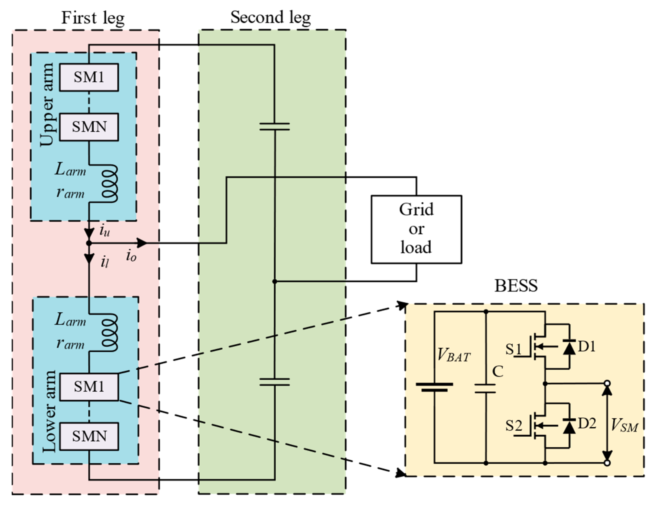
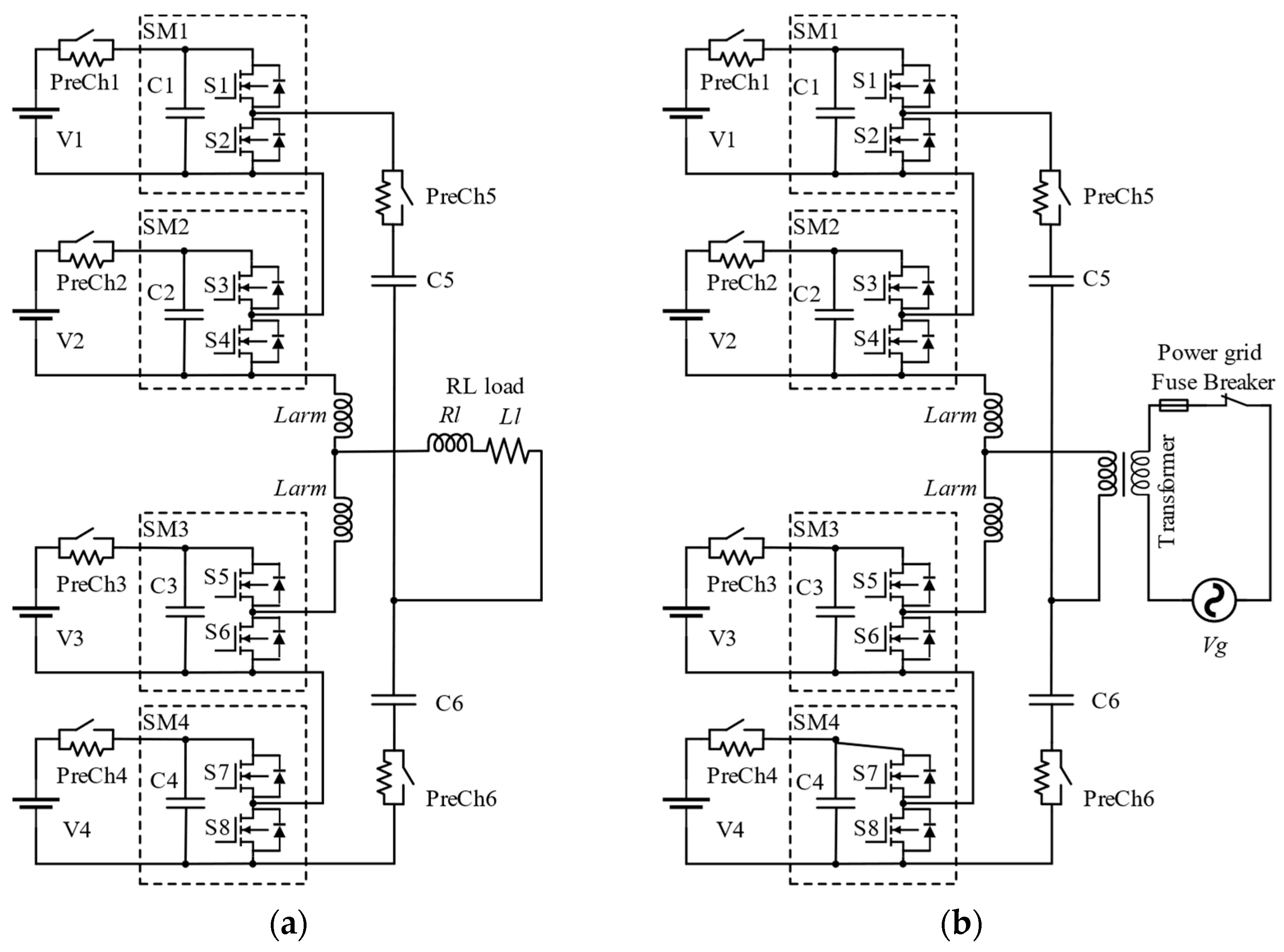
2.1. MMC-BESS Configuration

The schematic diagram of the single-phase MMC-BESS for residential UPS proposed in this paper is shown in Figure 1. This MMC-BESS consisted of two legs. One leg was formed by two symmetrical arms on the upper and lower sides, both constructed from a series of identical SMs and an arm inductor. The other leg was made up of two buck capacitor packs; SMs could be considered as well, similar to the first leg, when cost is not a concern. The arm inductor served multiple purposes: it reduced the current ripples of the converter, suppressed the circulating current, and improved the fault current ride-through ability of the converter. Each SM was composed of a battery pack, a capacitor, and a half-bridge circuit equipped with two semiconductors.

2.2. Mathematical Modeling

Suppose that each arm contains N SMs, and each SM battery pack has an identical voltage. In this case, the maximum voltage across each arm was V m a x = N V B A T . Based on Kirchhoff’s voltage law, the voltages of the upper and lower arms, i.e., v u and v l , are as described below [15,16]:
v u = 1 2 N V B A T v o v L a r m u
v l = 1 2 N V B A T + v o v L a r m l
where V B A T is the battery voltage and v o is the output voltage. Meanwhile, v L a r m u and v L a r m l denote the voltage drops across the upper and lower arm inductors, respectively. Considering that the resistance of the arm inductors is negligible, it is disregarded in this study. The voltage drop across the arm inductors can be expressed in terms of the derivative of the current flowing through them as follows:
v L a r m u = L a r m d i c i r d t + L a r m 2 d i o d t
v L a r m l = L a r m d i c i r d t L a r m 2 d i o d t
where i c i r represents the circulating current in the MMC-BESS converter, L a r m is the arm inductance, i o denotes the output current, and i c i r is the circulating current. The current flowing through the upper arm is defined as the upper arm current i u , while the current flowing through the lower arm is defined as the lower arm current i l . The relations among the MMC-BESS output current, circulating current, and upper/lower arm current are presented as follows:
i u = i c i r + i o 2
i l = i c i r x i o 2
i c i r = i u + i l 2
i o = i u i l
By substituting Equations (3)–(6), the external and internal dynamic equations of the MMC-BESS can be derived as follows [17]:
L a r m 2 d i o d t = v l v u 2 v o
L a r m d i c i r d t = 1 2 N V B A T v u + v l 2
As indicated in Equations (9) and (10), the output current can be controlled by adjusting the voltage difference between the upper-arm and lower- arm voltages. Meanwhile, the circulating current can be controlled by regulating the sum of the upper-arm and lower-arm voltages. Consequently, the voltage difference between the upper-arm and lower-arm voltages and the sum of these voltage contribute to the driving voltages of the output current and the circulating current, respectively. These driving voltages are represented as follows:
v o = v l v u 2 L a r m 2 d i o d t
v c i r = 1 2 N V B A T v u + v l 2
where v c i r is the circulating current driving voltage.
The charging and discharging of the battery packs are determined by the submodule switching events and the direction of the current. The corresponding battery current can be described using the battery’s SoC and capacity as follows:
i u k = Q B A T d S o C u k d t
i l k = Q B A T d S o C l k d t
where i u k and i l k denote the current flowing through the battery banks in the k-th SM of the upper arm and lower arm, respectively. Q B A T represents the battery capacity, and S o C u k and S o C l k are the corresponding SoC values of the k-th SM. Using S o C u k and S o C l k , the average upper arm SoC S o C ¯ u and the average lower arm SoC S o C ¯ l can be calculated. Also, the system average SoC S o C ¯ a v g can be obtained as follows:
S o C ¯ u = 1 N k = 1 N S o C u k
S o C ¯ l = 1 N k = 1 N S o C l k
S o C ¯ a v g = 1 2 S o C ¯ u + S o C ¯ l
Based on the assumption of ideal switches and battery packs, the power of the battery packs within each SM can be derived as per the method described in [18], which is presented as follows:
p u k = v S M u k i u = V B A T i u k = V B A T Q B A T d S o C u k d t
p l k = v S M l k i l = V B A T i l k = V B A T Q B A T d S o C l k d t
where p u k and p l k denote the battery power of the k-th SM in the upper arm and lower arm, respectively. The power of the upper arm and lower arm can be calculated as the sum of the power of all individual SMs in that arm. After substituting the relevant variables using Equations (15) and (16), the power can be presented as follows:
p u = k = 1 N N V B A T Q B A T d S o C u k d t = N V B A T Q B A T d S o C ¯ u d t
p l = k = 1 N N V B A T Q B A T d S o C l k d t = N V B A T Q B A T d S o C ¯ l d t
where p u and p l denote the power of the upper arm and lower arm, respectively. The power difference between the upper and lower arms can be derived as follows:
p = p u p l = N V B A T Q B A T d S o C ¯ u S o C ¯ l d t
As mentioned, the arm power can be calculated based on the battery voltage and current. In addition, it can be determined from the viewpoint of the arm voltage and arm current, as detailed below:
p u = 1 2 N V B A T v o L a r m d i u d t v u i u
p l = 1 2 N V B A T + v o L a r m d i l d t v l i l
Similarly, the arm power difference is obtained as follows [17,19]:
p = p u p l = 1 2 N V B A T i o 2 v o i c i r L a r m d i o i c i r d t
The right-hand sides of Equations (22) and (25) are equal. Assuming v o = V m sin ω t and i h = I h sin ω t φ , and neglecting the alternating terms, a new equation to describe the arm SoC can be derived as follows:
N V B A T Q B A T d S o C ¯ u S o C ¯ l d t V m I c i r 1 cos ϕ 1
Equation (26) suggests that the equilibrium of the SoC between the upper and lower arms can be achieved by modulating the fundamental component of the circulating current. Equation (26) provides the theoretical fundament for the upper-level arm SoC balancing control of the proposed two-level active SoC balancing control in this paper.

3. MMC-BESS Control Strategy

In this work, the multi-layer control system of the single-phase MMC-BESS consisted of multiple control objectives. These included controlling the output voltage and current, ensuring grid synchronization when integrated into the power grid, suppressing the circulating current, and equalizing the batteries SoCs. The output voltage and current regulation were structured with a dual-loop mechanism. The outer loop was dedicated to tuning the output voltage, and the inner loop focuses on controlling the output current. Regarding the circulating current, the control mechanism was designed to minimize the extraneous current that circulates within the converter. During the balanced state of the MMC-BESS, this circulating current can give rise to detrimental effects such as increased power dissipation and reduced energy conversion efficiency. The SoC equalization control was divided into two parts. One was focused on balancing the SoC across the arms, and the other aimed at equalizing the SoC of individual SMs. Thanks to the SoC equalization control, a uniform SoC was established both between the arms and among the SMs.

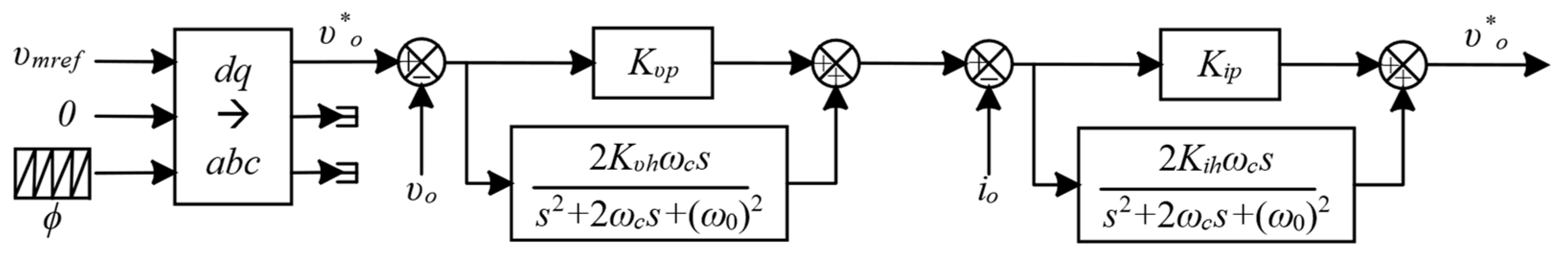
3.1. Dual-Loop Output Voltage and Current Control in Islanded Mode

The structure of the dual-loop output voltage and current control for the single-phase MMC in islanded mode with an RL load is depicted in Figure 2. This control strategy consisted of a voltage outer loop and a current inner loop. The voltage outer loop was responsible for detecting the output voltage and comparing it with the reference voltage v r e f to obtain the voltage error signal. To facilitate the application of this control in grid-related scenarios (even though it is in a non-grid application here, considering potential grid-connection adaptability), inverse Park conversion was employed. In this process, the reference voltage v r e f served as the d-component, while the q-component was set to zero. The voltage rotating angle was pre-stored in a lookup table, covering a range from 0 to 2 π . In this study, instead of the traditional proportional-resonant (PR) controller, the QPR controller was chosen. This selection was primarily because the QPR controller offers a broader bandwidth and is more feasible for practical implementation, as supported by the literature [20,21,22]. The transfer function of the QPR controller is as follows:
G v s = K v p + 2 K v h ω c s s 2 + 2 ω c s + ω 0 2
where K v p and K v h are the proportional and resonant coefficients of the voltage QPR controller, respectively; ω c is the cut-off frequency, which limits the bandwidth to avoid high-frequency noise; and ω 0 presents the resonant angular frequency. Here, it specifically represents the fundamental frequency, facilitating the precise control of the fundamental voltage signal.
The processed error signal served as the reference current of the current inner loop. The current inner loop takes i o * as the reference, detects the actual output current i o , and calculates the current error signal. The transfer function of its QPR controller is as follows:
G i s = K i p + 2 K i h ω c s s 2 + 2 ω c s + ω 0 2
where K i p and K i h are the proportional and resonant coefficients of the current QPR controller, respectively. At the fundamental frequency, the QPR controller of the current inner loop can achieve zero-steady-state error tracking, quickly and accurately adjust the current error, and output the control signal v o * to drive the switching devices, ensuring that the system outputs stable current and voltage.

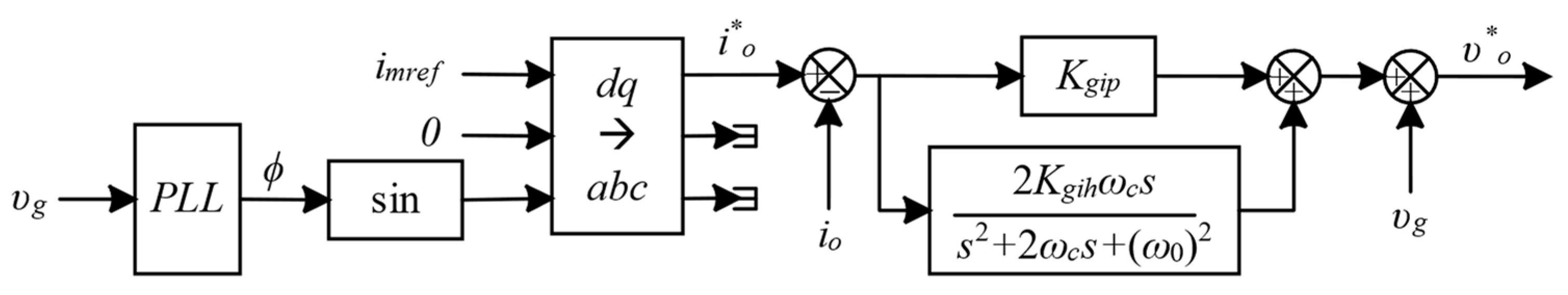
3.2. Grid-Connected Control

When the single-phase MMC-BESS was connected to the grid, the grid synchronization control became necessary. In this paper, to achieve effective grid synchronization, a phase-locked loop (PLL) proposed in [23] was employed. The input of the PLL was the grid voltage v g , and it output the grid rotating phase angle ϕ . This phase angle served as a fundamental reference for the entire control system, guiding subsequent operations such as coordinate transformation and current control. The sin module generated a sinusoidal signal based on the phase angle ϕ , which was fed into the inverse Park conversion module with the input current reference i r e f to generate the sinusoidal current reference i o * . In the grid current control loop, the QPR controller is used as
G i s = K i p + 2 K g i h ω c s s 2 + 2 ω c s + ω 0 2
where K g i p and K g i h are the proportional and resonant coefficients of the grid current QPR controller, respectively. In the calculation of the final output voltage reference value v o * , v g is involved to adjust its output based on the real-time state of the grid. When the grid voltage fluctuates, the control system monitors and analyzes v g , and dynamically adjusts the output voltage reference v o * . The block diagram of the grid-connected control is shown in Figure 3.

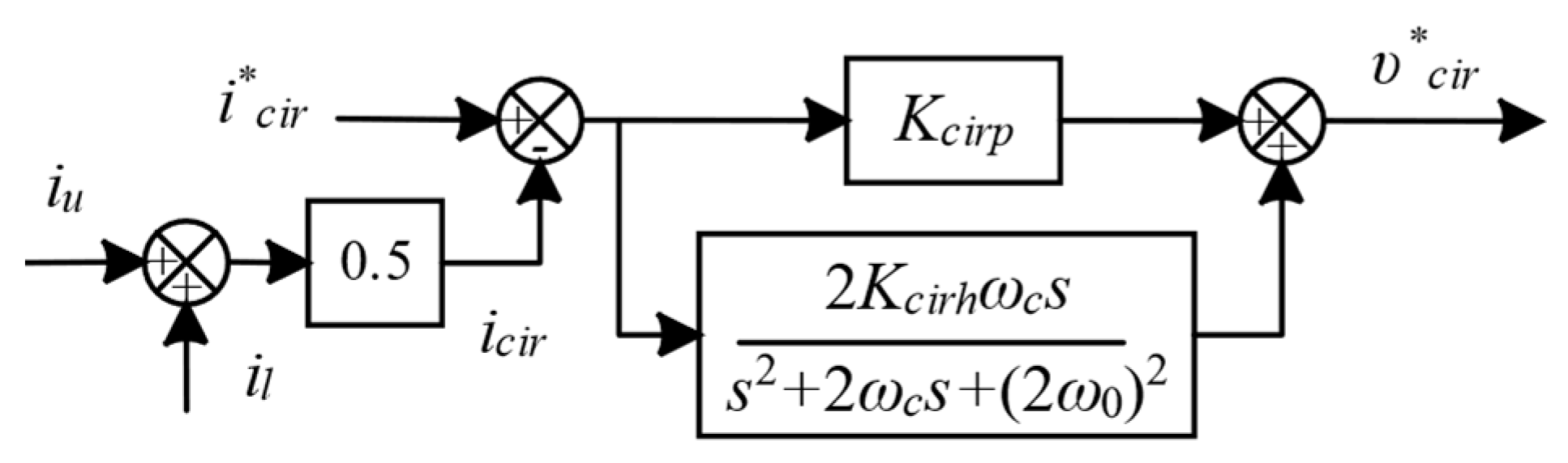
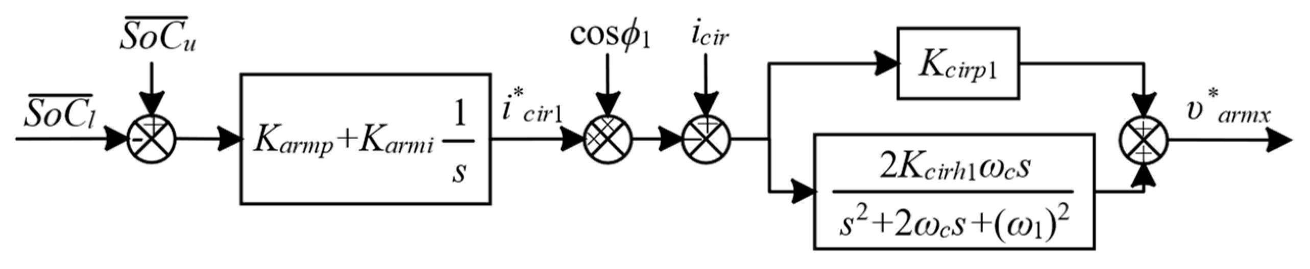
3.3. Circulating Current Control

In the steady balanced state, the circulating current leads to distortion in the arm current and incurs additional power losses. Hence, it is necessary to eliminate this circulating current. Although the arm inductor can suppress the circulating current to some extent [24], a dedicated active regulator is required for its complete elimination. Given that the circulating current is predominantly composed of second-order harmonics, the design of the eliminator mainly focuses on suppressing this harmonic component. The control block diagram for this process is presented in Figure 4. The transfer function of the QPR controller is given as follows:
G c i r s = K c i r p + 2 K c i r h ω c s s 2 + 2 ω c s + 2 ω 0 2
where K c i r p and K c i r h denote the proportional and resonant gains of the QPR controller, respectively.

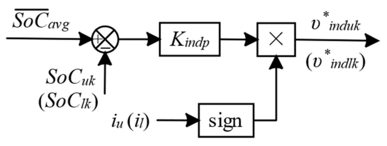
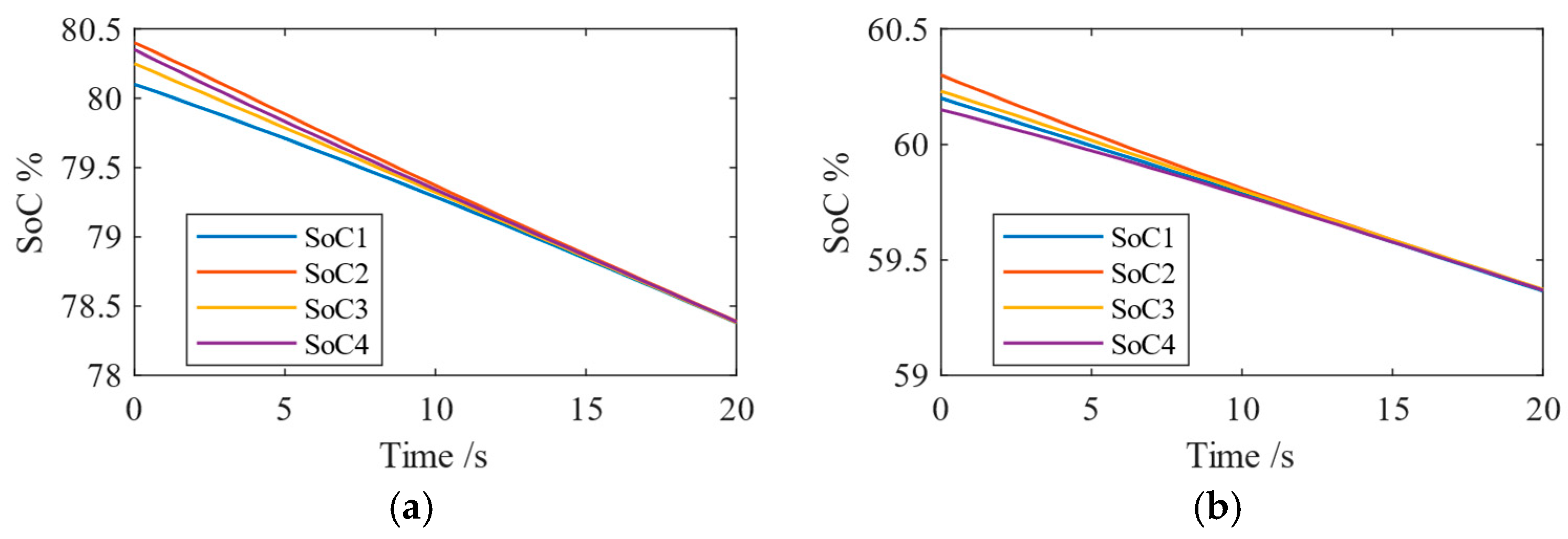
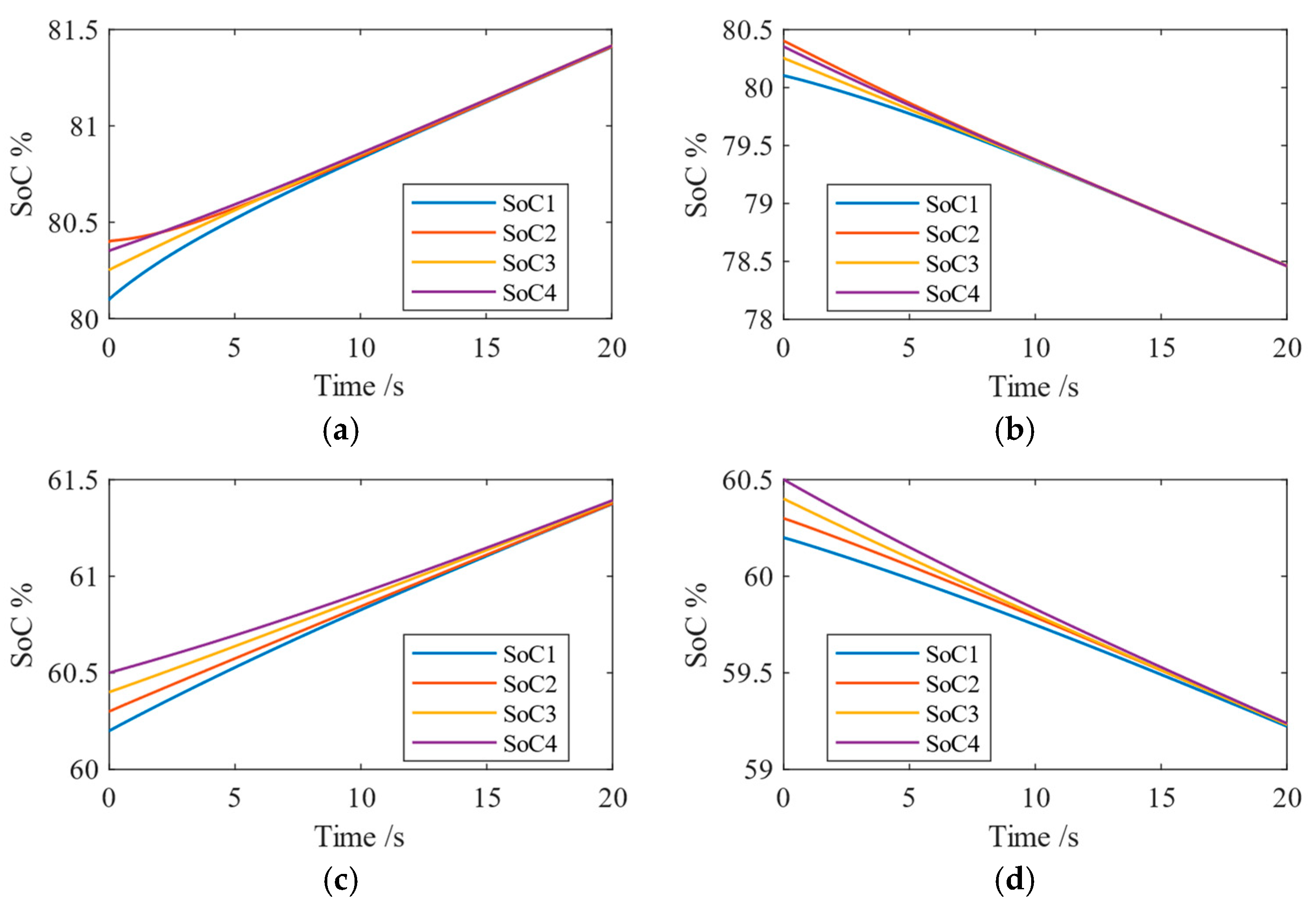
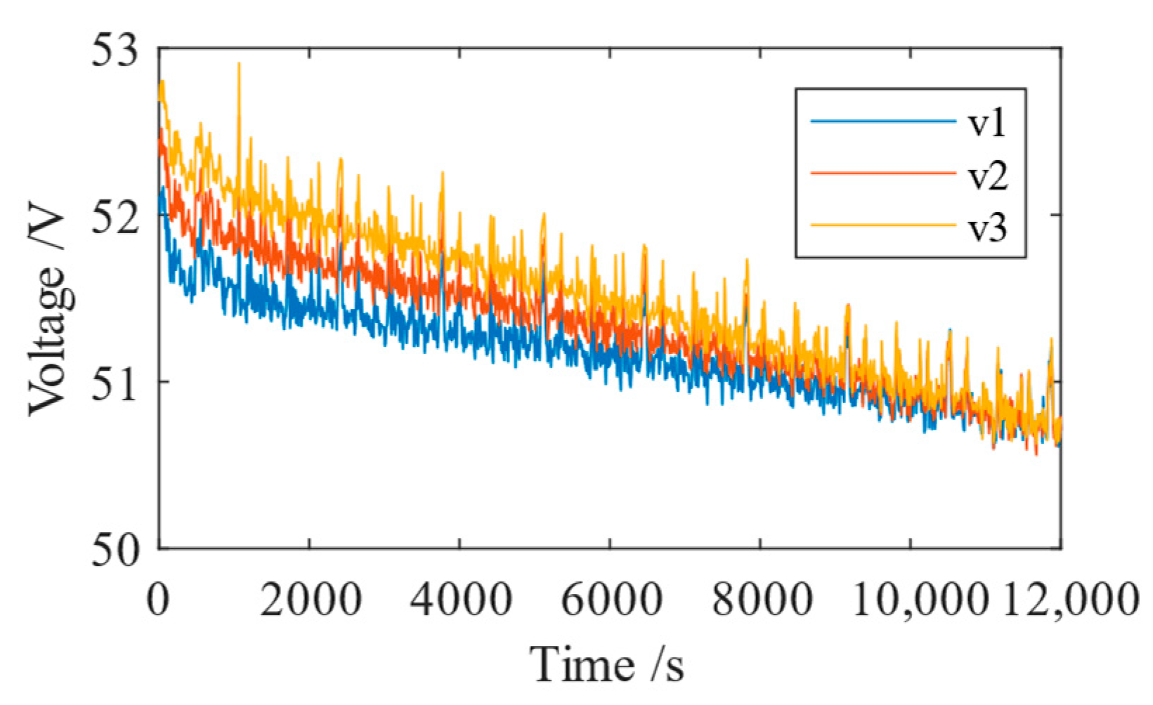
3.4. Two-Level Active SoC Balancing Control

The two-level SoC balancing control in this paper contained the upper-level arm SoC balancing control and the lower-level individual submodule SoC balancing control. With respect to the upper-level arm SoC equalization, the power was transferred from the arm with the greater SoC to the arm with lower SoC. The control scheme is visualized in Figure 5. As analyzed in Section 2 of mathematical modeling and indicated in Equation (26), the arm SoC balancing can be achieved by the fundamental circulating current, and therefore, the circulating current is added to compare with the reference generated by the SoC difference tunning PI controller. Similar to the output current controller, the QPR controller is adopted to regulate the fundamental harmonics. The operation and theoretical basis of the QPR controller will be thoroughly discussed in the following section of design and optimization of QPR controller, no further elaboration is presented here.
As for the lower-level individual SM SoC equalization, it was realized by a simple proportional controller, as shown in Figure 6. Notably, the sign of the arm current was taken into account to adjust the control signal.

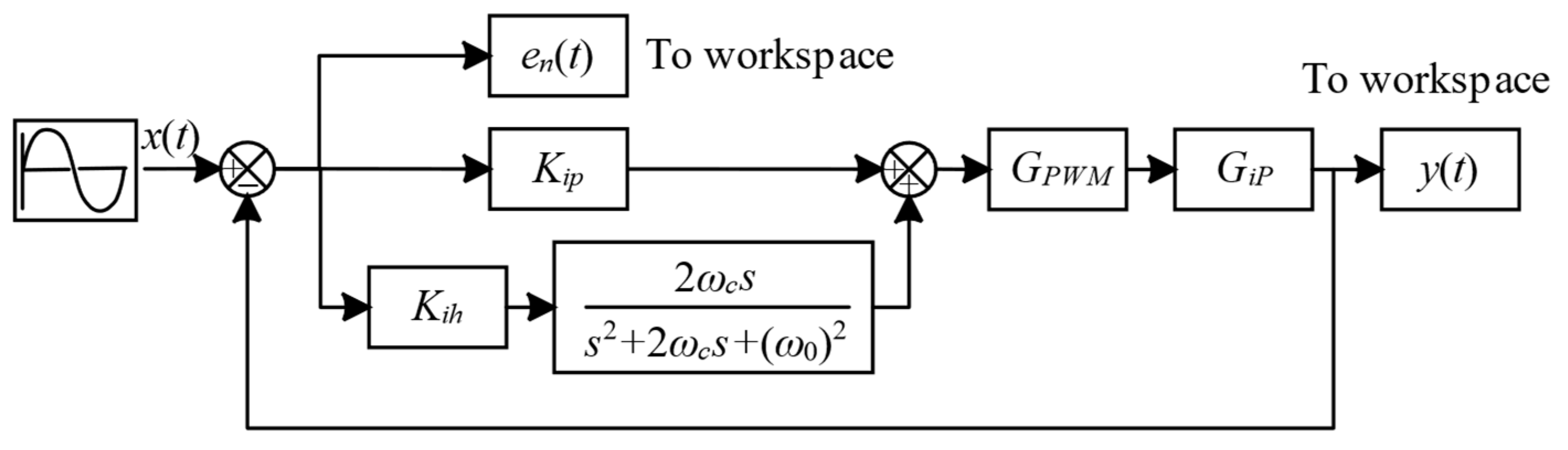
4. Design and Optimization of QPR Controller

Compared to PI and PR controllers, the QPR controller offers distinct advantages. PI controllers face difficulties in accurately tracking sinusoidal waveforms, while PR controllers have a narrow bandwidth, making them sensitive to frequency changes. In contrast, the QPR controller not only tracks sinusoidal reference with high accuracy but also has a broader bandwidth, enabling it to better tolerate frequency variations. Given these benefits, the QPR controller was the key technique used extensively in this paper. It played a vital role in essential areas like dual-loop output voltage and current control, circulating current control, and SoC balancing control, ensuring the high-performance and stable operation of the single-phase MMC-BESS. This paper analyzed and optimized the QPR controller by using the PSO optimization method. It first determined the boundaries of control gains to ensure system stability and appropriate control actions. Then, it evaluated the QPR controller’s performance in tracking sinusoidal references. Finally, the PSO method was applied to search for the optimal controller parameters within the defined gain boundaries, enhancing the QPR controller’s performance in tracking sinusoidal signals.

4.1. Boundaries of Control Gains

In terms of design and optimization of the QPR controller, take the output current controller as an example, the introduced cut-off frequency can prevent the QPR controller from losing sensitivity when there is a frequency shift. As per the information in [22], such a frequency shift should be kept within the range of ∆f = ±2%. Hence, the margin of the cut-off frequency can be determined as follows:
ω c 2 π f 0 × f
Here, with f 0 = 50 Hz, the margin for the cut-off frequency was set such that ω c 6.28 rad/s.
The plant transfer function of the output current is as follows:
G i P s = 2 L a r m s + r a r m
In order to obtain a satisfactory transient response and guarantee the system’s stability, the proportional gain K i p should be computed within a certain range. It is assumed that the modulation time delay is half of the sampling period T s . Thus, as stated in reference [22], the transfer function of the PWM can be formulated as follows:
G P W M s = e T s s 1 e T s s T s s
In an effort to simplify the calculation with an acceptable level of accuracy, the delay can be represented by poles and zeros through the application of the first-order Pade approximation. This approach is shown as follows:
e T s s 1 0.5 T s s 1 + 0.5 T s s
By substituting Equation (34) into Equation (33), an approximation of G P W M s can be obtained as follows:
G P W M s 1 0.5 T s s ( 1 + 0.5 T s s ) 2
Subsequently, the boundary of K i p can be determined based on the open-loop transfer function G i s G i P s G P W M s through the application of Routh’s stability criterion. Suppose G i s G i P s G P W M s = N ( s ) / D ( s ) , then the characteristic equation can be derived as follows:
D s + K N s = 0
where K represents the upper-limit boundary of the proportional coefficient K i p . With the assistance of the MATLAB symbolic solver, the boundary of K i p can be determined as follows:
K i p < 4 L a r m + 2 ω c L a r m T s + L a r m ω 0 2 T s 2 4 T s
To eliminate the steady-state errors in both phase and magnitude, an appropriate value for K i p needs to be chosen. The corresponding phase margin can be hypothesized as shown below, following the guidelines presented in [25]:
ϕ m = π 2 1.5 α c T s
where α c represents the crossover frequency. According to [26], the time constant can be roughly derived from the crossover frequency as follows:
τ i 10 α c  
Taking into account the relationship between the time constant and the proportional coefficient K i p , the resonant coefficient K i h can be estimated as follows:
K i h < K i p τ i   K i p ( π 2 ϕ m ) 30 T s
Assuming the arm inductance is 2.5 mH, the cut-off frequency is 5 rad/s, the sampling time of the QPR controller is 0.0001 s, and the phase margin is π / 4 rad, the upper limits of K i p and K i h can be calculated as 25 and 13069, respectively.

4.2. Performance Evaluation of Sinusoidal Reference

In terms of the evaluation of the performance of the controller, the criteria in the time domain performance are usually defined by the step response, i.e., the settling time t s e t and the maximum overshoot M 0 [27,28]. The step signal can be expressed as:
r t   = 0     t < 0                 r t   = r     t > 0
where r is a constant. The settling time is the minimum time at which the tracking error becomes sufficiently small:
t s e t = min t 1 e n ( t ) < ϵ                 t < t 1
where e n   t e t r is the normalized tracking error and ϵ is a user-defined tolerance which is usually defined between 0.02 and 0.05. The maximum overshoot is related to the maximum value of the output signal during its transient response to a step reference, which is given by:
M 0 = max M r r , 0
where M is the maximum value of the output signal. However, the input reference of the QPR controller is generally a sinusoidal signal. The definition given above to the step reference is not perfectly suitable for the sinusoidal reference. Therefore, the definition should be adapted to evaluate the performance of the resonant controller in response to the sinusoidal input signal. The adapted measures for the sinusoidal reference are investigated in [27]. Assume that the input sinusoidal waveform can be presented as:
r t   = 0     t < 0                 r t   = a r sin ω r t   t > 0
where a r is the amplitude of the sinusoidal signal. The settling time is obtained in the same way as in Equation (42) but it has e n   ( t ) e t a r . Instead of using time units to evaluate the settling time, it is replaced by the number of periods of the reference.
n s = t s e t ω r 2 π
In terms of the overshoot, it is redefined as:
M 0 = max M a r a r , 0

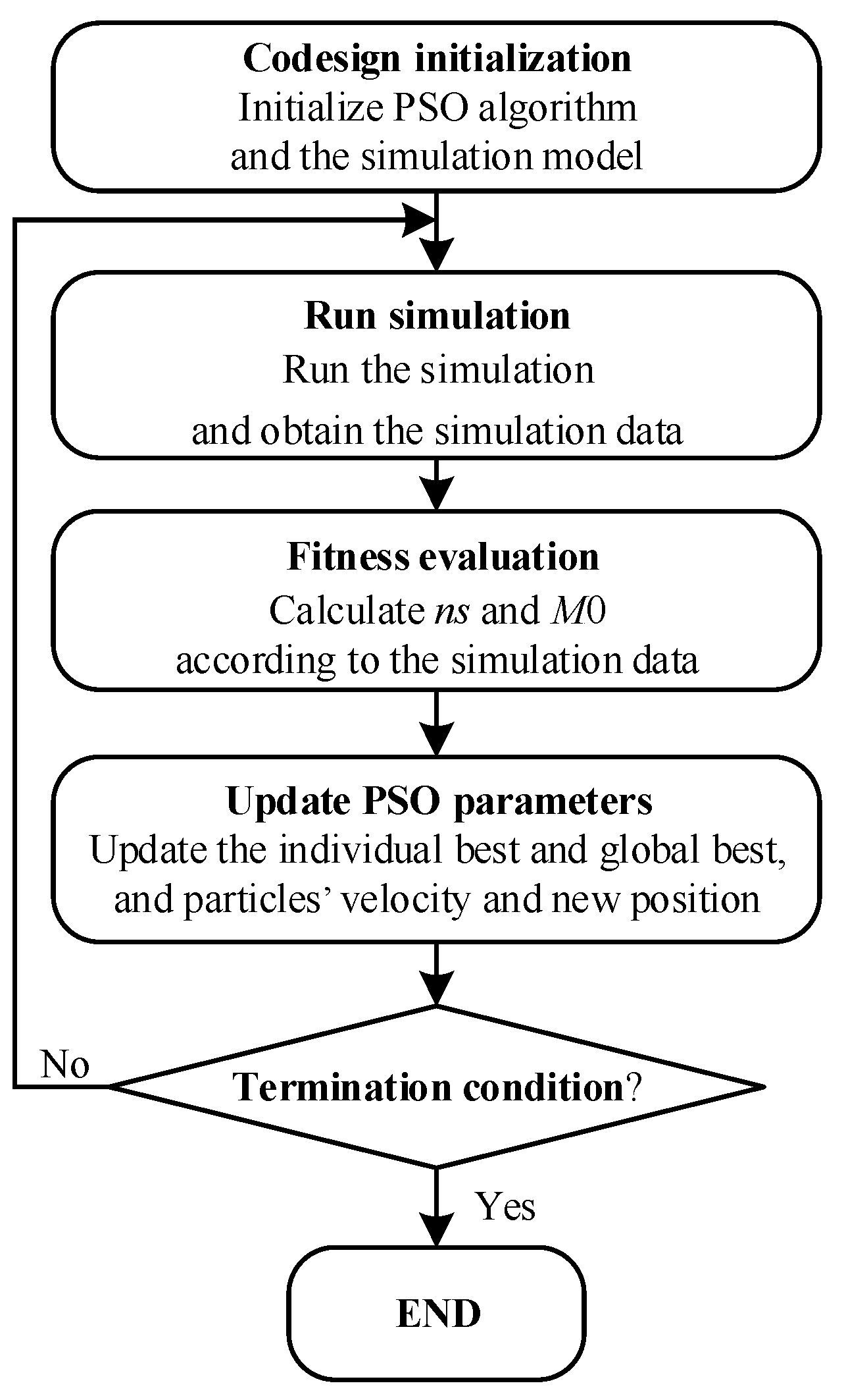
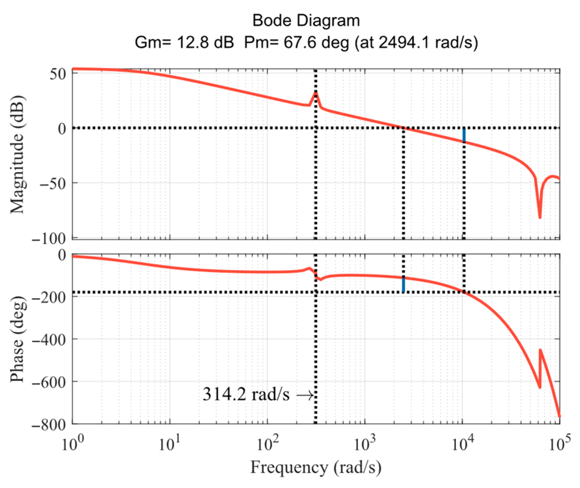
4.3. Optimization of QPR Controller

The PSO, motivated by the natural food searching behavior of birds, was selected as the optimization method of the QPR controller. The optimization was a codesign process in MATLAB/Simulink 2022b. The control model was first built in Simulink, as shown in Figure 7.
Since ω c is only used to select the bandwidth around the resonant frequency, to reduce the computation load, it is not considered as a variable in the optimization. Therefore, the adjustable parameters are the proportional coefficient K i p and integral coefficient K i h . The transfer functions of the PWM and the plant are defined by Equations (31) and (34). After the completion of each simulation, the output signal and error signal were sent to the MATLAB workspace where the PSO took the data and the optimization was run. The flowchart of the codesign optimization is shown in Figure 8:
Step 1. Code sign initialization: The optimization process commences with the initialization of the PSO algorithm and the simulation model. In this step, the fitness function and PSO parameters are initialized while considering the constraints and the swarm initialization. Each particle starts its search from a randomly assigned position with a certain velocity. These initial positions are regarded as the best positions for each particle initially, and the first globally optimal position is selected from them. This initial setup lays the foundation for the subsequent optimization.
Step 2. Run simulation: After the initialization, the simulation is executed to obtain the simulation data. This step is crucial for the optimization as it allows us to evaluate the impacts of different parameter settings through simulation. The data collected here will serve as the basis for the subsequent fitness evaluation.
Step 3. Fitness evaluation: Based on the simulation data, the error e n ( t ) and output y ( t ) are sent to workspace. According to Equations (42), (45), and (46), the performance of the controller can be evaluated in terms of the settling number of periods n s and overshoot M 0 . The fitness function of the PSO is defined as
f i t n e s s = min n s + M 0
The fitness value is assigned to each particle’s current position according to its coordinates. If this value exceeds the individual or global best values, the corresponding position is updated. This evaluation step helps in identifying the potentially optimal parameter combinations.
Step 4. Update PSO parameters: Following the fitness evaluation, the individual best and global best positions are updated. As the particles move, they compare the fitness at their current positions with the best fitness achieved so far. The position corresponding to the best fitness is defined as the individual optimal position. By re-evaluating each particle’s individual best position, the global best position is determined. Moreover, the velocity and position of the particles, which are key factors in the optimization, are updated. The velocity is adjusted based on the relative positions of the individual and global optima, enabling the particles to move towards more promising regions in the search space.
Step 5. Termination Condition: The algorithm will halt when either the maximum allowed number of iterations is reached or the fitness value remains unchanged over several consecutive iterations. If this termination condition is met, the optimization process stops; otherwise, it loops back to Step 2 to continue the search for better parameter settings.
The optimal parameters generated by the PSO algorithm were K i p = 25 and K i h = 113. Figure 9 shows the Bode plot of the output current open-loop transfer function G i s G i P s G P W M s . From the Bode plot, the output current control was stable with a gain margin of 12.8 dB and a phase margin of 67.6° at a frequency of 2494.1 rad/s. It was also shown from the Bode plot that the resonant frequency was 314.2 rad/s, aligning with the targeted fundamental frequency.

5. Simulation Results

To validate the proposed single-phase MMC-BESS and its control strategies, the simulation models were developed in MATLAB/Simulink®R2022b. In the simulation, two different grid voltages were considered, 311 V (peak value corresponding to an RMS value of 220 V) and 50 V. Specifically, the grid voltage with an RMS value of 220 V (peak value of approximately 311 V) represented the typical residential grid voltage, while the downsized 50 V was used for the experimental prototype test. Table 1 presents the specifications of the simulated single-phase MMC-BESS. The topology of the single-phase MMC is the same as shown in Figure 1. It had two SMs in each arm, and the battery nominal voltage of each SM was 400 V. The modulation technique was phase-shifted carrier-based pulse width modulation (PSC-PWM), and the carrier frequency was 20 kHz. Additionally, a downsized model was built with a nominal battery voltage of 50 V due to experimental constraints. To accelerate the simulation process, the capacity of the battery was set to 1 Ah. Simulations of the single-phase MMC-BESS for residential UPS applications were carried out under two operation modes: islanded mode with an RL load and grid-connected mode. The subsequent sections present the simulation results for these two scenarios.

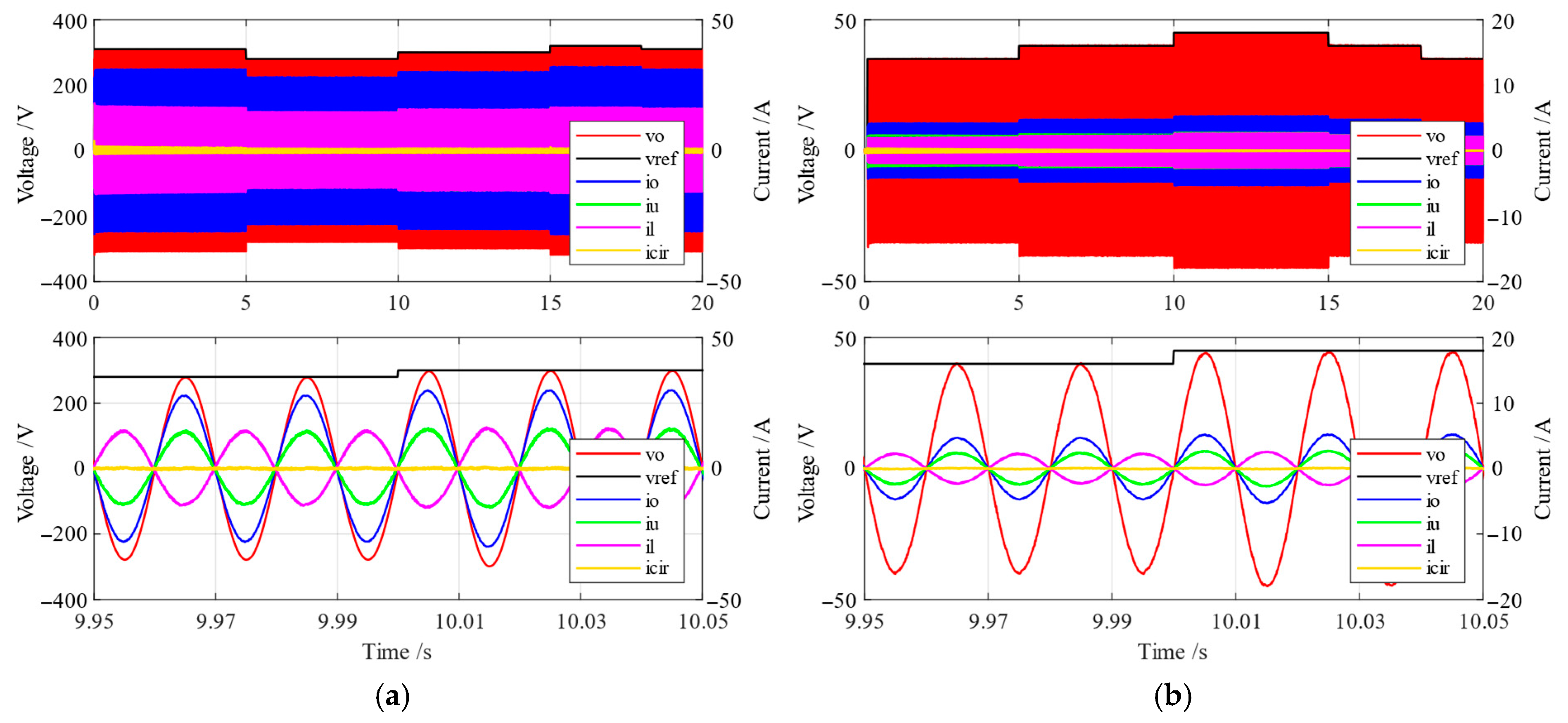
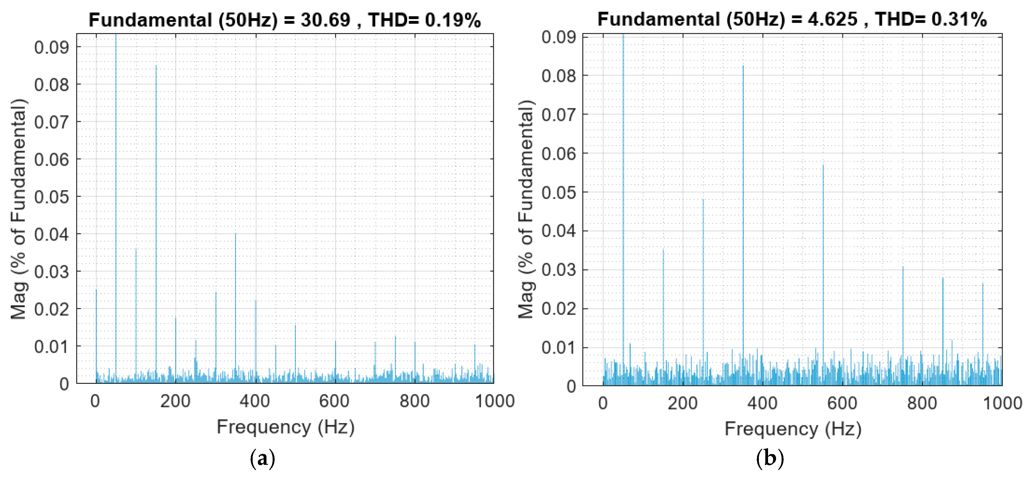
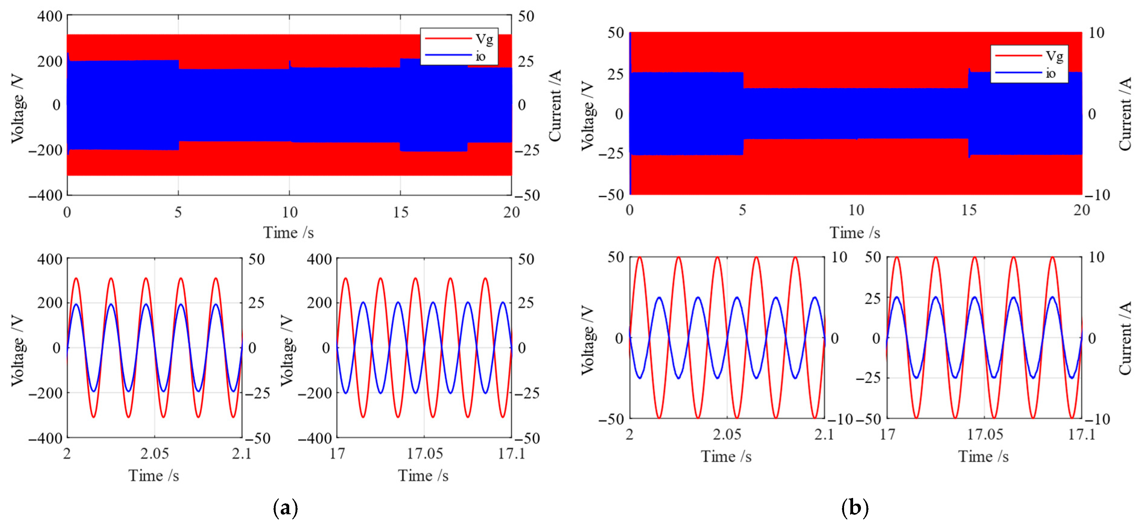
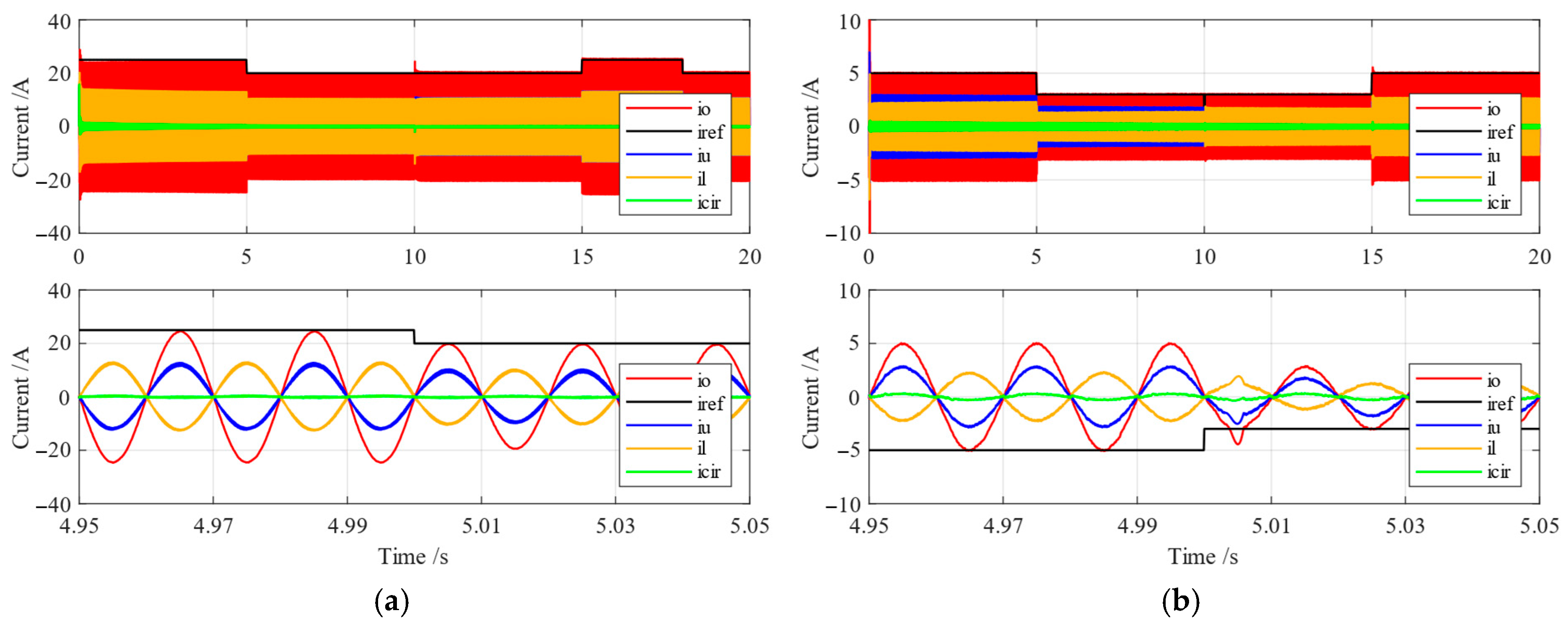
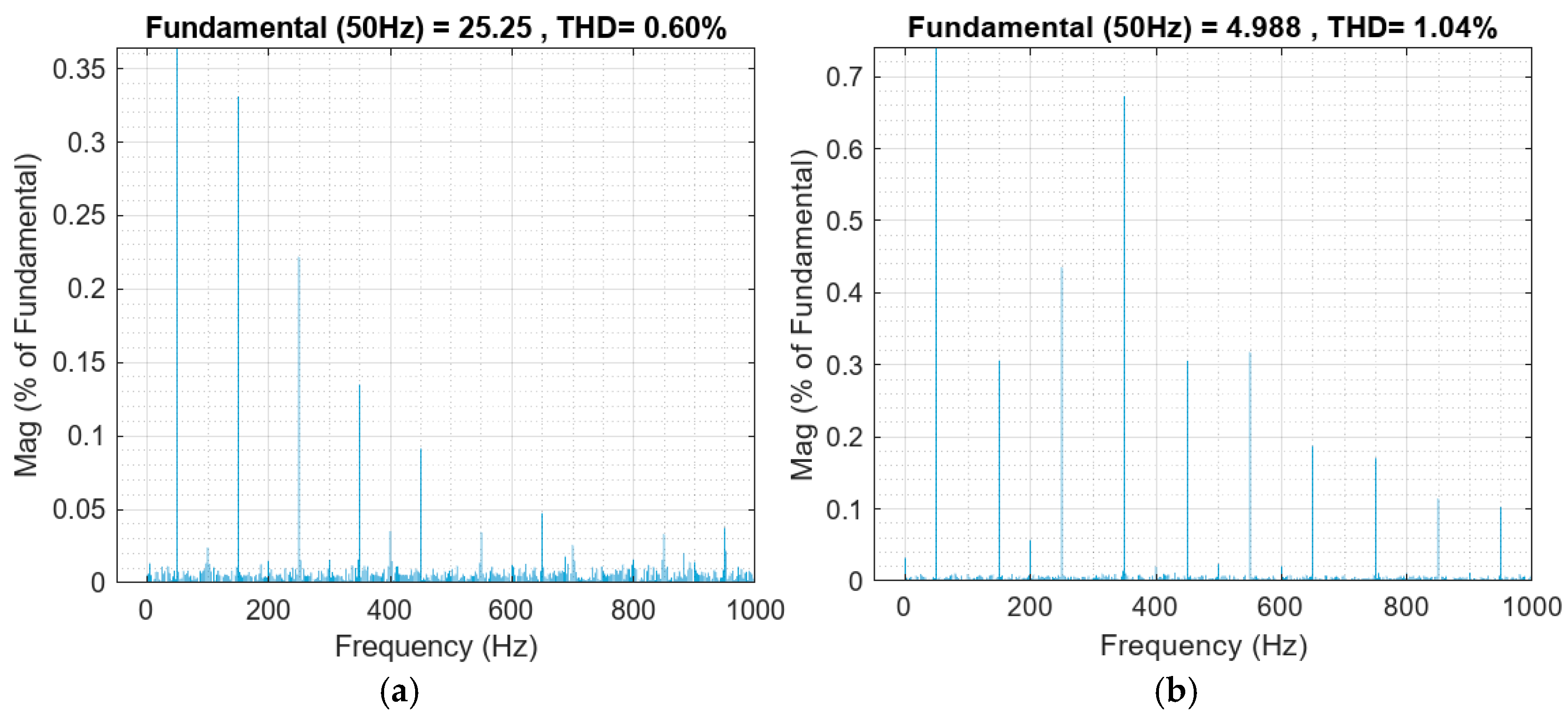
5.1. Simulation in Islanded Mode

In the single-phase MMC-BESS under islanded mode with an RL load, the control methods used in the model were dual-loop voltage and current control, circulating current control, arm balancing control and individual balancing control. The waveforms of the output voltage, output current, upper arm and lower arm current, and circulating current are shown in Figure 10. Figure 10a,b provide results for the full-scale model and the downsized model, respectively. The given reference was the voltage v r e f , shown as a black line. It was allocated to the outer loop voltage controller, which then generated the current reference for the inner current loop.
From Figure 10, it can be observed that the response of the voltage was fast where it took less than one cycle to follow the voltage reference. Since the dual-loop controller was used, the current reference was produced by the outer voltage controller. In the steady state of the full-scale model, the THD of the voltage was determined to be 0.04% and it was measured to be 0.19% for the current. For the downsized model, the calculated THD values of the voltage and current were 0.22% and 0.31%, respectively. The THD spectrum of the output current in islanded mode simulation of the full-scale and downsized models is shown in Figure 11. It can also be noted that the circulating current was eliminated to zero thanks to the circulating current control. Figure 12a,b show the SoC profiles with the RL load test of the full- and downsized models; it can be seen they were balanced after less than 20 s for both.

5.2. Simulation in Grid-Connected Mode

The single-phase MMC-BESS was connected to the grid and a PLL was added in the control system to synchronize with the grid. Under the control of the PLL, the grid rotating angle was generated and served as a reference in the subsequent current control. In the grid-connected simulation, the given reference was the current i r e f , shown as a black line in the following figures.
Figure 13 shows the grid voltage and current in the charging and discharging modes. Figure 13a,b provide results for the full-scale model and the downsized model, respectively. Similarly, Figure 12a shows the results of the full-scale model, while Figure 13b shows those of the downsized model. The currents are all shown in detail in Figure 14 including output current, upper/lower arm current, and circulating current of the full-scale model and down-sized model. The response time of the output current to track the reference value was less than one cycle and the steady state-error was minimized, as shown in Figure 14. The circulating current was controlled to around zero. For the full-scale model, the THD of the voltage was 0.02% and the THD of the current was 0.60%. For the downsized model, the THD values of the voltage and current were 0.02% and 1.04%, respectively. The THD spectrum of the grid current in grid-connected mode simulation of the full-scale and downsized models is shown in Figure 15.
Figure 16 presents the SoC profiles with the grid connection during the charging and discharging modes of the full-scale and downsized models. In both modes, the SoCs of the battery modules were balanced as expected.

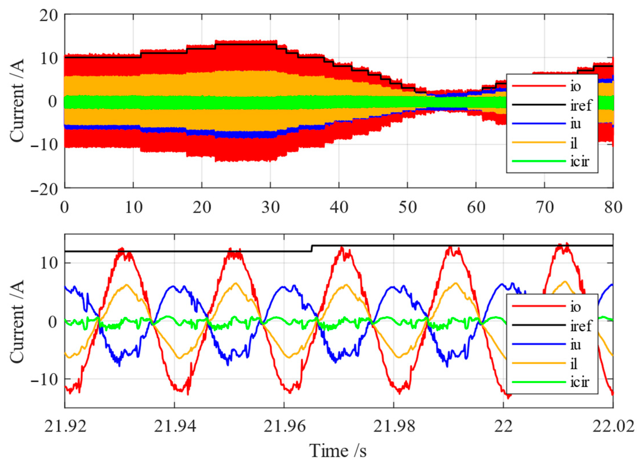
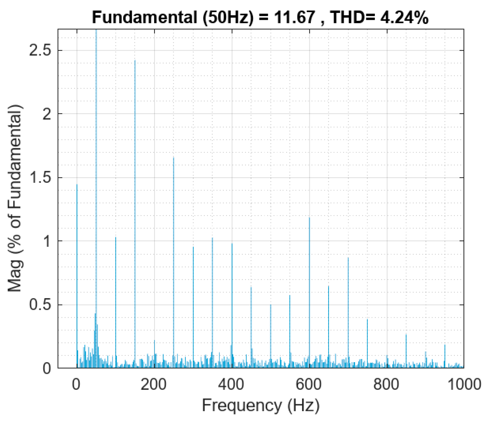
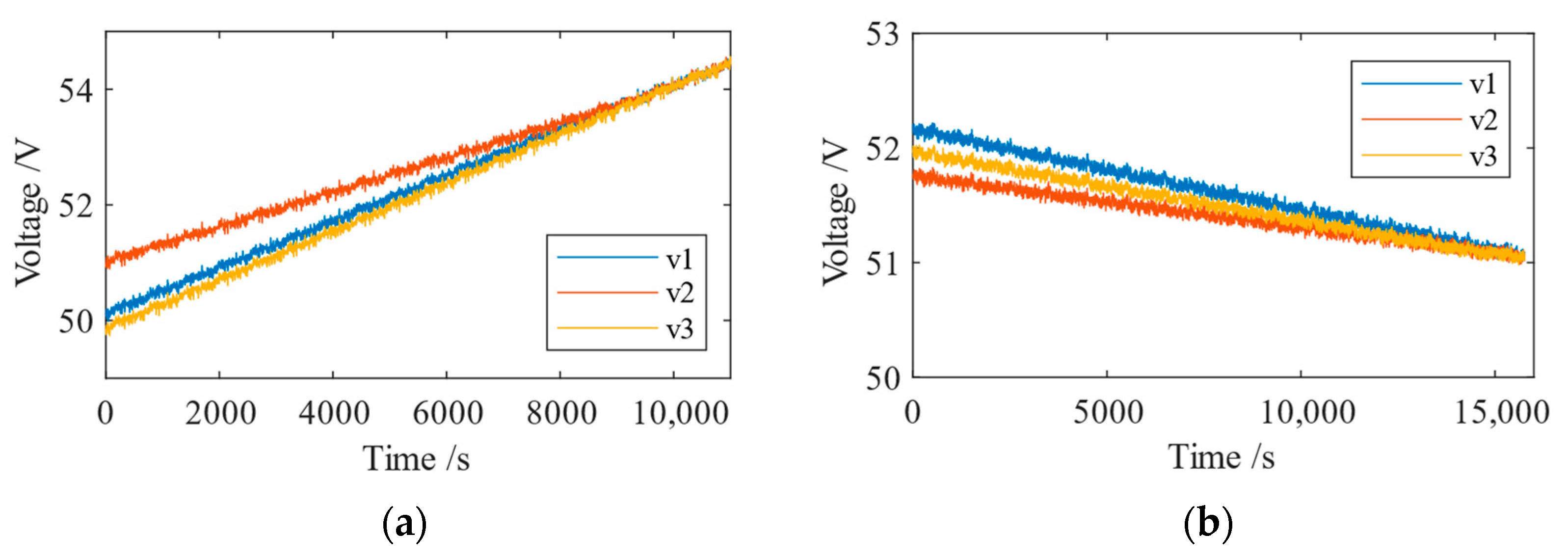
6. Experimental Results

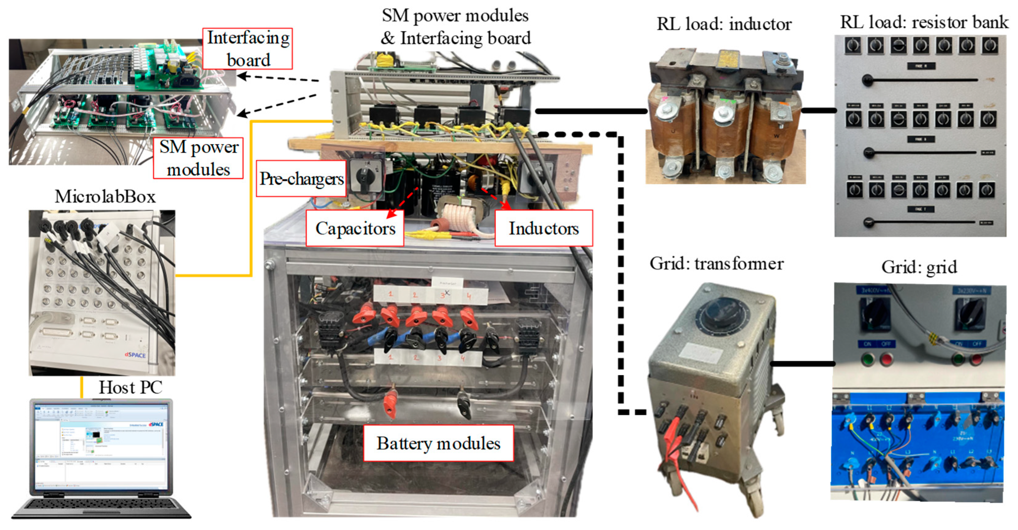
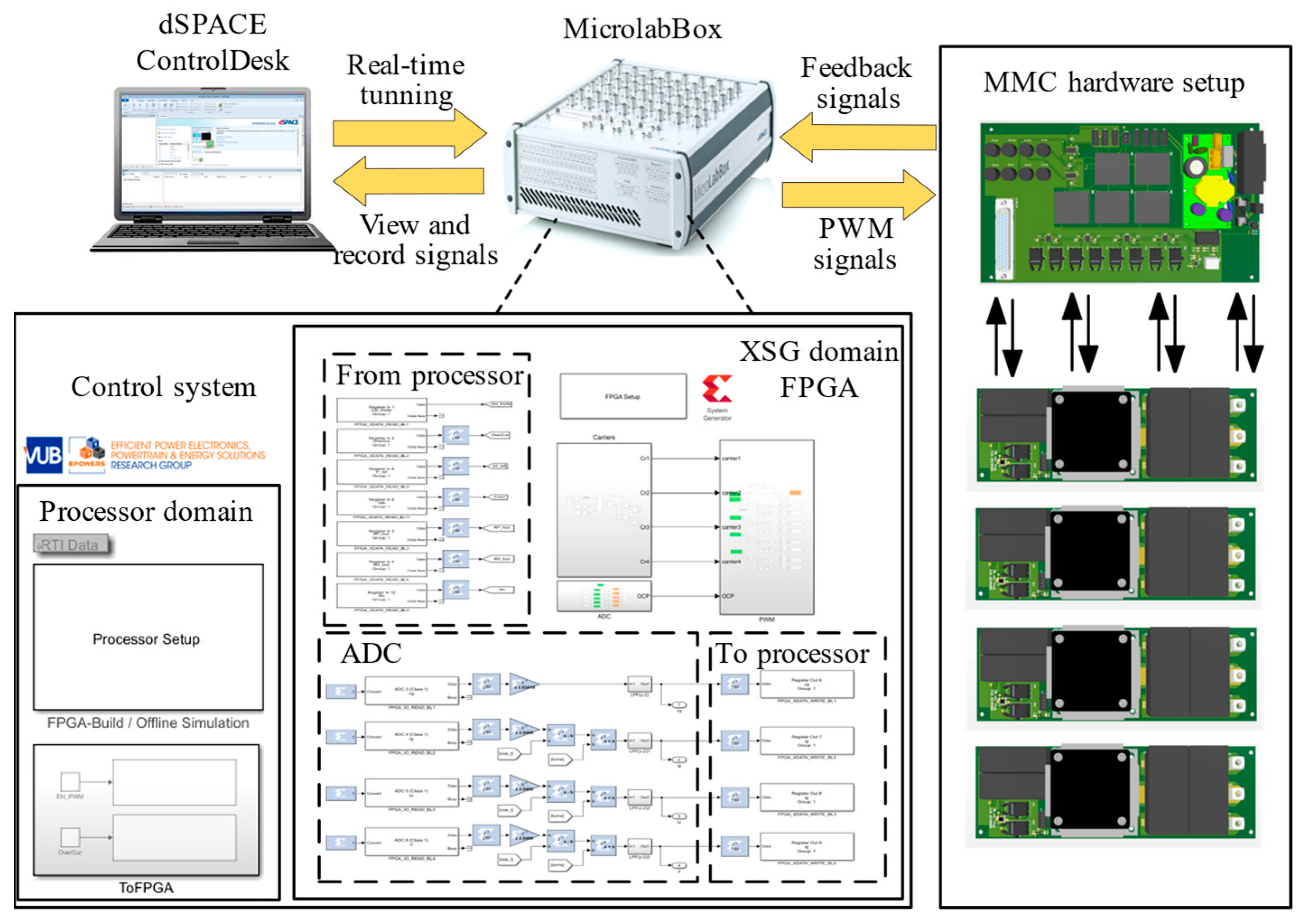
6.1. Experimental Prototype

To validate the proposed single-phase MMC-BESS, a prototype was built, and a series of experimental validations were carried out. In the prototype, the SiC MOSFET G3R20MT12K, due to its low price, high continuous drain current capability, small on-state resistance, and ample quantity in stock, was selected in this research. The gate driver was Wolfspeed CGD15SG00D2, which can convert the PWM signals to high level 15 V and low level −3.3 V.
The schematic diagram of the test circuits is shown in Figure 17. Three Li-ion NCA/NMC packs with a nominal voltage of 50.4 V were used together with a bidirectional adjustable DC voltage power supply in the lower arm. The single-phase MMC-BESS was tested both with RL load and grid connection, where V1, V2 and V3 were the battery modules, and V4 was the bidirectional DC voltage power supply. In this configuration, the DC bus voltage of the MMC-BESS was 200 V, i.e., 100 V in the upper arm and 100 V in the lower arm. The second leg was composed of buck capacitor packs. In order to limit the capacitor charging current and protect the battery modules, a pre-charge circuit composed of a switch and a resistor was positioned adjacent to each capacitor connection point. Other main parameters of the experimental test setup are listed in Table 2. Figure 18 shows the experimental test setup of the single-phase MMC-BESS with the RL load and grid. It should be noted that the battery modules were equipped with a battery management system, which transmitted the SoC data to the MicrolabBox via CAN communication. However, for practical reasons, the battery voltage was utilized in the balancing control in the subsequent part.
The controller was implemented on dSPACE MicroLabBox 2. The programming of the FPGA was facilitated by a Simulink plug-in design tool known as Xilinx System Generator (XSG) developed by Xilinx. Within this framework, high-level concepts modeled in Simulink can be translated into executable VHDL code through bitstream and implemented on the FPGA board of dSPACE MicroLabBox 2. The data communication was achieved by real-time blocks in the XSG domain. For the feedback signals, the signals measured by the sensors were sampled by the 16-bit Analog-Digital Conversion (ADC), with input voltage range [−10 V, 10 V]. dSPACE ControlDesk 7.1 was used to visualize and record the selected signals. A graphical user interface (GUI) was designed in dSPACE ControlDesk environment. The reference setpoint, PWM enable, and control parameters were set from the processor domain in real-time running, communicating with the FPGA board via local buses. The diagram of the real-time implementation is shown in Figure 19. An implementation of a part of the FPGA program in the XSG domain, such as the PSC-PWM, is shown in Figure 20. It used counters to generate the triangle carriers and employed delay blocks to generate the phase-shifted angle.

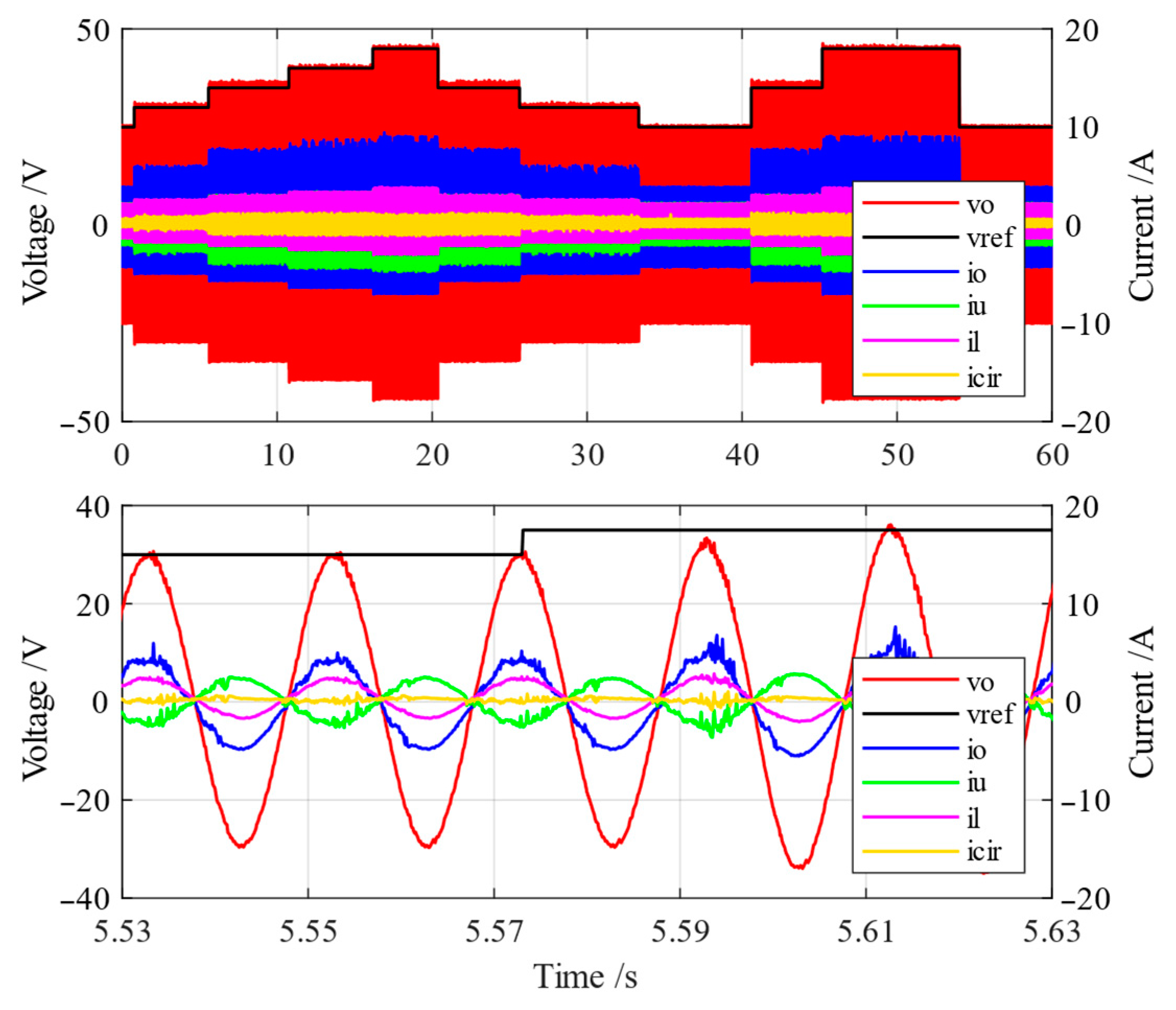
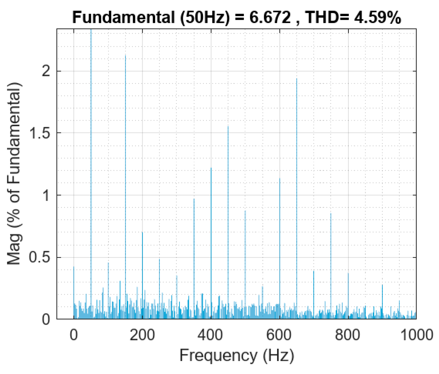
6.2. Experiment in Islanded Mode

The single-phase MMC-BESS was first tested with an RL load. The control methods included dual-loop voltage and current control, circulating current control, arm balancing control, and individual balancing control. As presented in Table 2, the experimental test setup of the RL load had four submodules in total, and three of them were connected to battery modules. The battery rated capacity was 58 Ah, and its nominal voltage was 50.4 V. The load inductance was 340 μH, and the load resistor was provided by an adjustable resistor bank, as shown in Figure 18. The waveforms of the output voltage, output current, upper arm and lower arm current, and circulating current are shown in Figure 21.
It was observed that it took approximately two cycles (0.04 s), to respond to the change in the voltage reference. Under steady-state conditions, the voltage can track the voltage reference. Since the dual-loop controller was used, the current reference was produced by the outer voltage controller. In the steady state, for example, starting at 5 s and for 20 cycles, the THD of the voltage was determined to be 1.37% and that of the current was 4.59%. It can also be noticed that the circulating current was eliminated to zero thanks to the circulating current control. The THD spectrum of the output current in islanded mode test is shown in Figure 22. Figure 23 shows the voltage profiles tested with the RL load, and the voltages among the battery modules reached an equilibrium state by using 12,000 s.

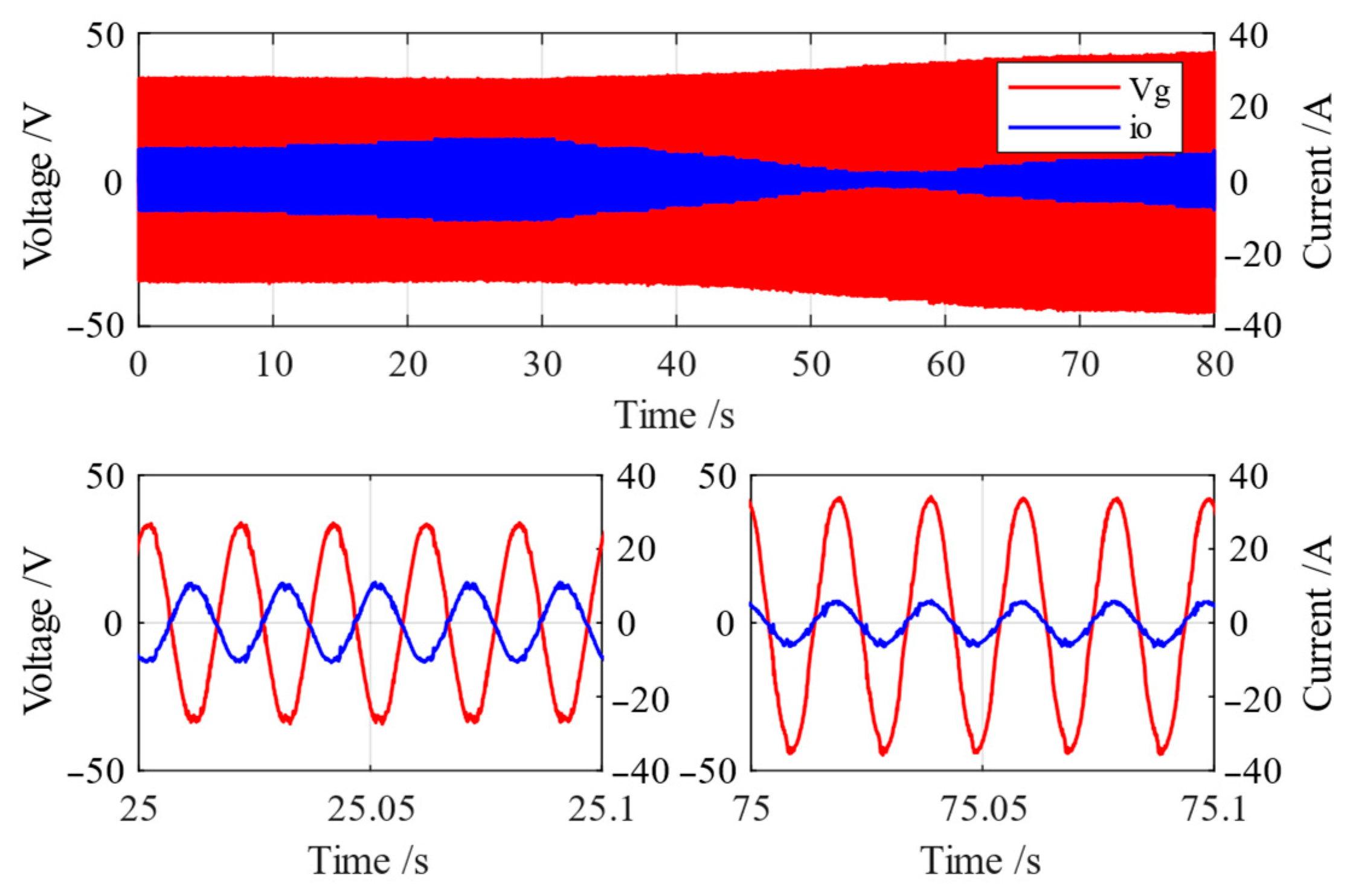
6.3. Experiment in Grid-Connected Mode

The single-phase MMC-BESS was also tested with grid connection, using a transformer for isolation and adjusting the grid voltage. Figure 24 shows grid voltage and current in the charging and discharging modes. The displacement power factor was calculated as 0.995 and 0.993 in these two modes, respectively.
The currents are all shown in detail in Figure 25, including output current, upper/lower arm current, and circulating current. Similar to the RL load test, the response time of the output current to track the refence value was approximately 0.04 s (two cycles), and the steady state error was minimized. The circulating current was controlled to around zero. The THD of the voltage and current during the steady state interval starting at 21 s and for 20 cycles were 1.72% and 4.24%, respectively. The THD spectrum of the grid current in grid-connected mode test is shown in Figure 26.
Figure 27 presents the voltage profiles obtained from tests with the grid during the charging and discharging modes. In both modes, the voltages of the battery modules can be balanced.

7. Conclusions

This paper has presented a single-phase MMC-BESS for residential UPS applications with two-level active SoC balancing control and optimized QPR controllers. The MMC-BESS configuration and its mathematical model were established, forming a basis for control strategy design. Control strategies including dual-loop output voltage and current control in islanded mode, grid-connected control, circulating current control, and SoC balancing effectively ensured stable operation. Simulations in islanded and grid-connected modes verified its basic operating characteristics. The experimental prototype and tests further confirmed the practicality of the proposed system. The experimental results show that, for both islanded and grid-connected tests, the balancing was achieved; and the response time to track the reference value took two cycles (0.04 s); the THD of the voltage was 1.37% and that of the current was 4.59% in the islanded mode test; and these values were 1.72% and 4.24% for voltage and current, respectively, in the grid-connected mode test.

Author Contributions

Conceptualization, Y.W., T.G., and O.H.; methodology, Y.W.; investigation, Y.W., T.G., and O.H.; writing—original draft, Y.W.; writing—review and editing, Y.W., T.G., and O.H.; supervision, T.G. and O.H.; funding acquisition, O.H. All authors have read and agreed to the published version of the manuscript.

Funding

This research was sponsored by the China Scholarship Council (Grant No. 201908500121). This research has received funding from the European Union’s Horizon Europe Research and Innovation program under Grant Agreement No. 101075496 (SiC4GRID). The views and opinions expressed are, however, those of the author(s) only and do not necessarily reflect those of the European Union or the European Climate, Infrastructure and Environment Executive Agency (CINEA). Neither the European Union nor the granting authority can be held responsible for them.

Data Availability Statement

Data are contained within the article.

Acknowledgments

The authors acknowledge the China Scholarship Council (CSC grant) for sponsoring this PhD research. This research has also received funding from the European Union’s Horizon Europe Research and Innovation program under Grant Agreement No. 101075496 (SiC4GRID). The authors also acknowledge Flanders Make for their support to our research group.

Conflicts of Interest

The authors declare no conflicts of interest.

References

  1. Yearly Electricity Data | Ember. Available online: https://ember-energy.org/data/yearly-electricity-data/ (accessed on 16 December 2024).
  2. Share of Electricity Production from Renewables. 2023. Available online: https://ourworldindata.org/grapher/share-electricity-renewables (accessed on 16 December 2024).
  3. Statistical Review of World Energy. Available online: https://www.energyinst.org/statistical-review (accessed on 16 December 2024).
  4. International Energy Agency. Batteries and Secure Energy Transitions. Available online: www.iea.org (accessed on 23 April 2024).
  5. Shamshuddin, M.A.; Kennel, R.M.; Verdugo, D. Nomenclature Overview and Beat Frequency in the Family of AC/AC Modular Multilevel Cascade Converters (MMCC). IEEE Access 2025, 13, 42064–42082. [Google Scholar] [CrossRef]
  6. Aslanian, M.; Neyshabouri, Y.; Raki, A.; Iman-Eini, H.; Liserre, M. A Fault-Tolerant Method Based on a Modified Selective Harmonic Mitigation Technique for Modular Multilevel Converter. IEEE Trans. Ind. Electron. 2024, 71, 12890–12899. [Google Scholar] [CrossRef]
  7. Gao, X.; Tian, W.; Yang, Q.; Chai, N.; Rodriguez, J.; Kennel, R.; Heldwein, M.L. Model Predictive Control of a Modular Multilevel Converter Considering Control Input Constraints. IEEE Trans. Power Electron. 2024, 39, 636–648. [Google Scholar] [CrossRef]
  8. Salvadores, T.; Pereda, J.; Rojas, F. Power Imbalance Analysis of Modular Multilevel Converter with Distributed Energy Systems. IEEE Open J. Ind. Electron. Soc. 2024, 5, 109–121. [Google Scholar] [CrossRef]
  9. Wang, Y.; Chakraborty, S.; Geury, T.; Hegazy, O. Modeling and Control of a Modular Multilevel Converter Based on a Battery Energy Storage System with Soft Arm State-of-Charge Balancing Control. Energies 2024, 17, 740. [Google Scholar] [CrossRef]
  10. Soong, T.; Lehn, P.W. Evaluation of Emerging Modular Multilevel Converters for BESS Applications. IEEE Trans. Power Deliv. 2014, 29, 2086–2094. [Google Scholar] [CrossRef]
  11. de Lucena, M.P.; Gehrke, C.S.; da Silva, I.R.F. Modular Multilevel Converter for High-Performance UPS Systems. In Proceedings of the 2021 Brazilian Power Electronics Conference, COBEP 2021, João Pessoa, Brazil, 7–10 November 2021. [Google Scholar] [CrossRef]
  12. Mhiesan, H.; Al-Sarray, M.; Mackey, K.; McCann, R. High Step-Up/Down Ratio Isolated Modular Multilevel DC-DC Converter for Battery Energy Storage Systems on Microgrids. In Proceedings of the IEEE Green Technologies Conference, Kansas City, MO, USA, 6–8 April 2016; pp. 24–28. [Google Scholar] [CrossRef]
  13. Trusova, E.S.; Dobroskok, N.A.; Lavrinovskiy, V.S.; Simukhin, V.I. Comparison of Efficiencies of Modular Multilevel and Classic UPS Structures. In Proceedings of the 2022 Conference of Russian Young Researchers in Electrical and Electronic Engineering, Saint Petersburg, Russia, 25–28 January 2022; pp. 897–900. [Google Scholar] [CrossRef]
  14. Trusova, E.S.; Simukhin, V.I.; Lavrinovskiy, V.S.; Fedorkova, A.O. Determining the Reliability of a UPS Based on a Modular Multilevel Converter. In Proceedings of the Seminar on Electrical Engineering, Automation and Control Systems: Theory and Practical Applications, EEACS 2023, Saint Petersburg, Russia, 23–25 November 2023; pp. 319–321. [Google Scholar] [CrossRef]
  15. Wang, Y.; Aksoz, A.; Geury, T.; Ozturk, S.B.; Kivanc, O.C.; Hegazy, O. A review of modular multilevel converters for stationary applications. Appl. Sci. 2020, 10, 7719. [Google Scholar] [CrossRef]
  16. Du, S.; Dekka, A.; Wu, B.; Zargari, N. Modular Multilevel Converters: Analysis, Control, and Applications; John Wiley & Sons: Hoboken, NJ, USA, 2017. [Google Scholar] [CrossRef]
  17. Quraan, M. Modular Multilevel Converter with Embedded Battery Cells for Traction Drives. Ph.D. Thesis, University of Birmingham, Birmingham, UK, 2016. [Google Scholar]
  18. Fan, S.; Zhang, K.; Xiong, J.; Xue, Y. An improved control system for modular multilevel converters featuring new modulation strategy and voltage balancing control. In Proceedings of the 2013 IEEE Energy Conversion Congress and Exposition, ECCE 2013, Denver, CO, USA, 15–19 September 2013; pp. 4000–4007. [Google Scholar] [CrossRef]
  19. Quraan, M.; Yeo, T.; Tricoli, P. Design and Control of Modular Multilevel Converters for Battery Electric Vehicles. IEEE Trans. Power Electron. 2015, 31, 507–517. [Google Scholar] [CrossRef]
  20. An, Q.; Zhang, J.; An, Q.; Shamekov, A. Quasi-Proportional-Resonant Controller Based Adaptive Position Observer for Sensorless Control of PMSM Drives Under Low Carrier Ratio. IEEE Trans. Ind. Electron. 2020, 67, 2564–2573. [Google Scholar] [CrossRef]
  21. Geng, S.; Gan, Y.; Li, Y.; Hang, L.; Li, G. Novel Method for Circulating Current Suppression in MMCs Based on Multiple Quasi-PR Controller. In Proceedings of the 2016 IEEE Applied Power Electronics Conference and Exposition (APEC), Long Beach, CA, USA, 20–24 March 2016; pp. 3560–3565. [Google Scholar] [CrossRef]
  22. Ye, T.; Dai, N.; Lam, C.S.; Wong, M.C.; Guerrero, J.M. Analysis, Design, and Implementation of a Quasi-Proportional-Resonant Controller for a Multifunctional Capacitive-Coupling Grid-Connected Inverter. IEEE Trans. Ind. Appl. 2016, 52, 4269–4280. [Google Scholar] [CrossRef]
  23. Karimi-Ghartemani, M.; Iravani, M.R. A new phase-locked loop (PLL) system. In Proceedings of the 44th IEEE 2001 Midwest Symposium on Circuits and Systems. MWSCAS 2001, Dayton, OH, USA, 14–17 August 2001; pp. 421–424. [Google Scholar] [CrossRef]
  24. Wang, Y.; Chakraborty, S.; Geury, T.; Hegazy, O. Inductance and Power Losses Analysis of an Arm Inductor for a Modular Multilevel Converter. In Proceedings of the IEEE Vehicle Power and Propulsion Conference (VPPC), Milan, Italy, 24–27 October 2013; pp. 1–6. [Google Scholar] [CrossRef]
  25. Parikh, H.R.; Martin-Loeches, R.S. Control of Modular Multilevel Converter (MMC) based HVDC application under unbalanced conditions. In Master, Energy Technology; Aalborg University: Aalborg, Denmark, 2016. [Google Scholar]
  26. Holmes, D.G.; Lipo, T.A.; Mcgrath, B.P.; Kong, W.Y. Optimized Design of Stationary Frame Three Phase AC Current Regulators. IEEE Trans. Power Electron. 2009, 24, 2417–2426. [Google Scholar] [CrossRef]
  27. Pereira, L.F.A.; Bazanella, A.S. Tuning Rules for Proportional Resonant Controllers. IEEE Trans. Control. Syst. Technol. 2015, 23, 2010–2017. [Google Scholar] [CrossRef]
  28. Henz Mossmann, B.; Alves Pereira, L.F.; Gomes da Silva, J.M., Jr. Tuning of Proportional-Resonant Controllers Combined with Phase-Lead Compensators Based on the Frequency Response. J. Control. Autom. Electr. Syst. 2021, 32, 910–926. [Google Scholar] [CrossRef]
Figure 1. Schematic diagram of the single-phase MMC-BESS for residential UPS.
Energies 18 01776 g001
Figure 2. Block diagram of the dual-loop output voltage and current control in islanded mode.
Energies 18 01776 g002
Figure 3. Block diagram of the grid-connected control.
Energies 18 01776 g003
Figure 4. Block diagram of the circulating current control.
Energies 18 01776 g004
Figure 5. Block diagram of the upper-level arm SoC balancing control.
Energies 18 01776 g005
Figure 6. Block diagram of the lower-level individual SoC balancing control.
Energies 18 01776 g006
Figure 7. Optimization process of the QPR controller in MATLAB/Simulink.
Energies 18 01776 g007
Figure 8. Flowchart of the codesign optimization based on PSO algorithm.
Energies 18 01776 g008
Figure 9. Bode plot of the output current open-loop transfer function.
Energies 18 01776 g009
Figure 10. Voltage and current waveforms of the single-phase MMC-BESS in islanded mode simulation with an RL load: (a) the full-scale model; (b) the downsized model. (Red line—output voltage v o ; black line—reference voltage v r e f ; blue line—output current i o ; green line—upper arm current i u ; purple line—lower arm current i l ; yellow line—circulating current i c i r ).
Energies 18 01776 g010
Figure 11. THD of output current of the single-phase MMC-BESS in islanded mode simulation with an RL load: (a) the full-scale model; (b) the downsized model.
Energies 18 01776 g011
Figure 12. SoC profiles of the battery modules of the single-phase MMC-BESS in islanded mode simulation with an RL load: (a) the full-scale model; (b) the downsized model.
Energies 18 01776 g012
Figure 13. Grid-side voltage and current from charging mode to discharging mode of the single-phase MMC-BESS in grid-connected mode simulation: (a) the full-scale model; (b) the downsized model. (Red line—grid voltage v g ; blue line—output current i o ).
Energies 18 01776 g013
Figure 14. Grid current, arm current, and circulating current of the single-phase MMC-BESS in grid-connected mode simulation: (a) the full-scale model; (b) the downsized model. (Red line—output current i o ; black line—reference current i r e f ; blue line—upper arm current i u ; yellow line—lower arm current i l ; green line—circulating current i c i r ).
Energies 18 01776 g014
Figure 15. THD of grid current of the single-phase MMC-BESS in grid-connected mode simulation: (a) the full-scale model; (b) the downsized model.
Energies 18 01776 g015
Figure 16. SoC profiles of the battery modules of the single-phase MMC-BESS in grid-connected mode simulation: (a) in the charging mode of the full-scale model; (b) in the discharging mode of the full-scale model; (c) in the charging mode of the downsized model; and (d) in the discharging mode of the downsized model.
Energies 18 01776 g016
Figure 17. Schematic diagram of the half-bridge single-phase MMC-BESS for residential UPS: (a) islanded mode; (b) grid-connected mode.
Energies 18 01776 g017
Figure 18. Experimental test setup of the single-phase MMC-BESS in islanded mode with an RL load and grid-connected mode.
Energies 18 01776 g018
Figure 19. Real-time test implementation process.
Energies 18 01776 g019
Figure 20. Real-time test implementation of the PSC-PWM.
Energies 18 01776 g020
Figure 21. Voltage and current waveforms of the single-phase MMC-BESS in islanded mode test with an RL load: red line—output voltage v o ; black line—reference voltage v r e f ; blue line—output current i o ; green line—upper arm current i u ; purple line—lower arm current i l ; yellow line—circulating current i c i r .
Energies 18 01776 g021
Figure 22. THD of output current of the single-phase MMC-BESS in islanded mode test with an RL load.
Energies 18 01776 g022
Figure 23. Voltage profiles of the battery modules of the single-phase MMC-BESS in islanded mode test with an RL load.
Energies 18 01776 g023
Figure 24. Grid-side voltage and current from charging mode to discharging mode of the single-phase MMC-BESS in grid-connected mode test: red line—grid voltage v g ; blue line—output current i o .
Energies 18 01776 g024
Figure 25. Grid current, arm current, and circulating current of the single-phase MMC-BESS in grid-connected mode test: red line—grid voltage v g ; blue line—grid angle ω t ; red line—output current i o ; black line—reference current i r e f ; blue line—upper arm current i u ; yellow line—lower arm current i l ; green line—circulating current i c i r .
Energies 18 01776 g025
Figure 26. THD of grid current of the single-phase MMC-BESS in grid-connected mode test.
Energies 18 01776 g026
Figure 27. Voltage profiles of the battery modules of the single-phase MMC-BESS in grid-connected mode test: (a) in the charging mode; (b) in the discharging mode.
Energies 18 01776 g027
Table 1. Specification of the simulated single-phase MMC-BESS.
ParametersValues
No. of SMs per arm2
Nominal voltage of battery banks400 V/50 V
Battery capacity1 Ah
Rated power5 kW
Grid peak voltage311 V/50 V
Grid frequency50 Hz
Modulation techniquePSC-PWM
Carrier frequency20 kHz
SM capacitance100 μF
Arm capacitance480 μF
Arm inductance 2.5 mH
Sampling time0.0001 s
Table 2. Parameters of the experimental test setup.
ParametersValuesParametersValues
No. of SM power units4Battery-rated capacity58 Ah
No. of interfacing board1Arm inductance2.5 mH
No. of battery modules3No. of buck capacitors6
Battery chemistryLi-ion NCA/NMCCapacitance of buck capacitors160 μF
Battery nominal voltage50.4 VLoad inductance340 μH
Disclaimer/Publisher’s Note: The statements, opinions and data contained in all publications are solely those of the individual author(s) and contributor(s) and not of MDPI and/or the editor(s). MDPI and/or the editor(s) disclaim responsibility for any injury to people or property resulting from any ideas, methods, instructions or products referred to in the content.

