Article

Three-Level All-SiC High-Frequency High-Voltage Plasma Power Supply System

by
Kaida Cai
,
Jing Xiao
*,
Zhe Yang
and
Ranghao Hu
School of Mechanical and Electrical Engineering, Guilin University of Electronic Technology, Guilin 541004, China
*
Author to whom correspondence should be addressed.
Energies 2025, 18(7), 1617; https://doi.org/10.3390/en18071617
Submission received: 22 February 2025 / Revised: 14 March 2025 / Accepted: 20 March 2025 / Published: 24 March 2025
(This article belongs to the Special Issue High-Power Electronic Device Technologies and Its Applications)

Abstract

:
Plasma power supplies are extensively utilized in various manufacturing and medical industries. Addressing the challenges of high-voltage and high-temperature resistance in current plasma power supply systems under high-frequency conditions, this study proposes a novel design method for an all-SiC high-frequency high-voltage plasma power supply system based on a three-level topology. Firstly, the design encompasses a three-level high-frequency inverter main circuit, a three-level high-frequency control main circuit, and a high-frequency high-voltage transformer. Subsequently, a high-frequency high-voltage plasma power supply system, equipped with a rotary motor, was developed and experimentally validated. Finally, the system achieved a stable power output with a frequency of 25 kHz, an output voltage of 21.03 kV, and an output power of 13.42 kW. The experimental results demonstrate that the plasma power supply system exhibits stable output voltage and maintains an operating temperature under high-frequency and high-voltage conditions.

1. Introduction

Plasma power supplies are critical components in industrial as well as medical equipment. With the rapid development of modern power electronics technology, the inverter, as a key device for energy conversion and control, plays a vital role in the power system. Especially in the application field of plasma generators, the performance of the inverter directly impacts the stability of the whole system.
Although traditional full-bridge inverters are cost-effective and structurally simple, they have shortcomings in high-voltage and high-temperature resistance compared to three-level inverters. Full-bridge inverters, which use four switching devices to convert DC voltage to AC voltage, are commonly used in low-power applications such as household appliances and small electronic devices. However, their performance is inferior to that of three-level inverters in high-voltage and high-power applications. In contrast, the three-level inverter, a mainstream multilevel inverter topology, offers superior output voltage quality and efficiency. By dividing the DC voltage into three levels using two intermediate capacitors and four switching devices, the three-level inverter generates higher-quality output voltage with lower current harmonics and higher efficiency. This design also reduces switching device losses and electromagnetic interference (EMI) noise, making it particularly suitable for high-power applications.
To further enhance efficiency, the development of low-loss, high-performance semiconductor switching devices is crucial. Traditional Si-based inverters struggle to meet modern industrial demands for high efficiency and power density, particularly in high-temperature environments. In contrast, third-generation semiconductor materials such as SiC exhibit superior voltage resistance (>1200 V), thermal stability (up to 180 °C), and switching efficiency (reduced losses by 40% compared to Si devices) [1]. In plasma generators, SiC-based power semiconductor devices can significantly improve system power density and efficiency.
With the rapid progress of modern economy and science, high-voltage high-power converters have become a focal point in power electronics research. Despite advancements in switching device voltage-withstand levels, traditional two-level converters still struggle to meet the demands of medium- and high-voltage high-power applications [2,3]. Multilevel circuits, with their high device voltage withstand levels and low output-voltage harmonics, have garnered increasing attention [4]. Among these, the three-level circuit, first proposed by A. Nabae et al. in the 1980s [5], has been widely adopted in medium-voltage and high-power applications due to its simple structure and convenient control [6,7].
Multilevel inverters offer several advantages over two-level inverters, including reduced voltage stress on MOSFETs, lower harmonic content in the output voltage, and reduced EMI caused by du/dt. As a result, multilevel inverters are increasingly used in high-voltage and high-power applications [8]. For this reason, in this paper, a three-level topology is used instead of the traditional two-level full-bridge inverter to achieve high-voltage and high-power output.
The widely used switching devices in the market nowadays have always relied on the use of silicon material but the performance of silicon material is basically close to its theoretical limit [9,10]. Moreover, Si-based inverters are gradually unable to meet the requirements of high power density and high-temperature resistance in today’s industry, and new material SiC devices have emerged.
Compared to Si MOSFETs, SiC MOSFETs offer a higher breakdown voltage strength, lower loss, and higher thermal conductivity, making them suitable for high-voltage, high-switching-frequency, and high-power-density scenarios. As mass production increases, the cost–performance ratio of SiC devices becomes more favorable, leading to higher utilization rates [11]. For this reason, this paper employs SiC MOSFETs instead of Si MOSFETs in the T-bridge arms to reduce switching losses, enabling high-temperature and high-voltage resistance performance at higher switching frequencies.
Table 1 shows the research status of high-frequency and high-voltage plasma power supply systems at home and abroad. According to review [12], Krishna T.N. and Sathishkumar P. et al. designed the 4T analog MOSFETs, controlling the high-voltage high-frequency plasma power supply with a frequency of 25 kHz, an output voltage of 10 kV, and a power of 5 kW.
In the work of [13], the experimentations have been conducted based on high-voltage and high-frequency sinusoidal power supply. This generator can provide a peak sinusoidal voltage of up to 20 kV and a frequency range of 10–60 kHz for dielectric barrier discharge (DBD) loads, with a maximum output power of 200 W.
In this research paper [14], Cai X. and Fu Z. et al. presented a plasma power supply with a maximum output power of 1 kW, a frequency range of 20–50 kHz, and an output voltage of 3.2 kV, which is applied to the plasma load for cleaning machines.
In the present study [15], a high-voltage high-frequency plasma power supply for the reactor’s ignition was presented, which produces a frequency of 10–25 kHz and an output voltage of 14 kV.
According to Table 1, the current plasma schemes mostly adopt the half-bridge or full-bridge topology structure designed by traditional silicon-based power devices. These schemes cannot simultaneously achieve high-voltage and high-power output with the voltage exceeding 20 kV and power exceeding 10 kW under high-frequency operation. This article intends to use a three-level inverter topology based on silicon carbide MOSFETs to achieve high-voltage and high-power output with voltages exceeding 20 kV and powers exceeding 10 kW.
The purpose of this paper is to discuss the design and development of a plasma power supply system by combining the advantages of the three-level inverter as well as the third-generation semiconductor SiC material [16]. Section 2 describes in detail the design of the high-frequency high-voltage plasma power supply system, including the overall structure of the high-frequency high-voltage plasma power supply hardware system [17], the design of the three-level high-frequency inverter main circuit, the design of the three-level high-frequency control main circuit, and the design of the high-frequency high-voltage transformer [18]. Section 3 shows the analysis of the experimental results, demonstrating the three-level PWM drive signal source, busbar voltage signal, busbar current signal, transformer output signal analysis, and the operating temperature and power of the plasma power supply system. Finally, Section 4 discusses the potential value and application prospects of the three-level all-SiC high-frequency high-voltage plasma power supply system.

2. The Design of High-Frequency High-Voltage Plasma Power Supply

2.1. Overall Structure of High-Frequency High-Voltage Plasma Power Supply Hardware System

The system design of the high-frequency high-voltage plasma power supply is shown in Figure 1 [19], which is mainly composed of a three-level high-frequency inverter main circuit, a three-level high-frequency control main circuit, and a high-frequency high-voltage transformer boost circuit [20]. A single-phase AC power supply (220 V) serves as the input. The AC voltage is rectified via a diode full-bridge circuit, generating a peak-to-peak DC output of 310 V. The SiC-based three-level high-frequency inverter main circuit converts it into a three-level output voltage signal. The drive control module generates dual complementary PWM drive signals at a high frequency of 25 kHz to drive the MOSFETs of the three-level inverter main circuit, enabling the inverter function. A high-frequency high-voltage transformer, designed with a ferrite PL-13 U core, is placed at the output of the main inverter circuit. The three-level output voltage signal is connected to the primary side of the transformer, and at the secondary side, the signal is boosted to a high voltage of 21.03 kV, which is connected to a plasma rotary gun where gas forms plasma [21]. The following describes the main circuits:
  • Inverter main circuit: the system uses an NPC diode-clamped three-level inverter as the main circuit of the system to convert DC power to AC power;
  • MCU control system: this generates a PWM drive signal to drive the switching tube on and off so that the inverter main circuit outputs AC power to realize the inverter function. This design adopts the MCU control system based on an ARM 32-bit Cortex-M4F microcontroller AT32F403ARCT7 developed by Chongqing, China as the core [22];
  • Isolation circuit: the MCU control system and the drive circuit are electrically isolated to ensure that the control signals generated by the MCU control system are not interfered with by the strong external electric parts [23], which stabilizes and guarantees the safe operation of the MCU control system [24];
  • Drive circuit: the PWM signal generated by the MCU control system is amplified to drive the switching tube of the inverter main circuit and it is used to turn MOSFETs on and off.
Table 2 shows the peak-to-peak technical specifications for the design of the high-frequency high-voltage plasma power supply system.

2.2. Design of the Three-Level High-Frequency Inverter Main Circuit

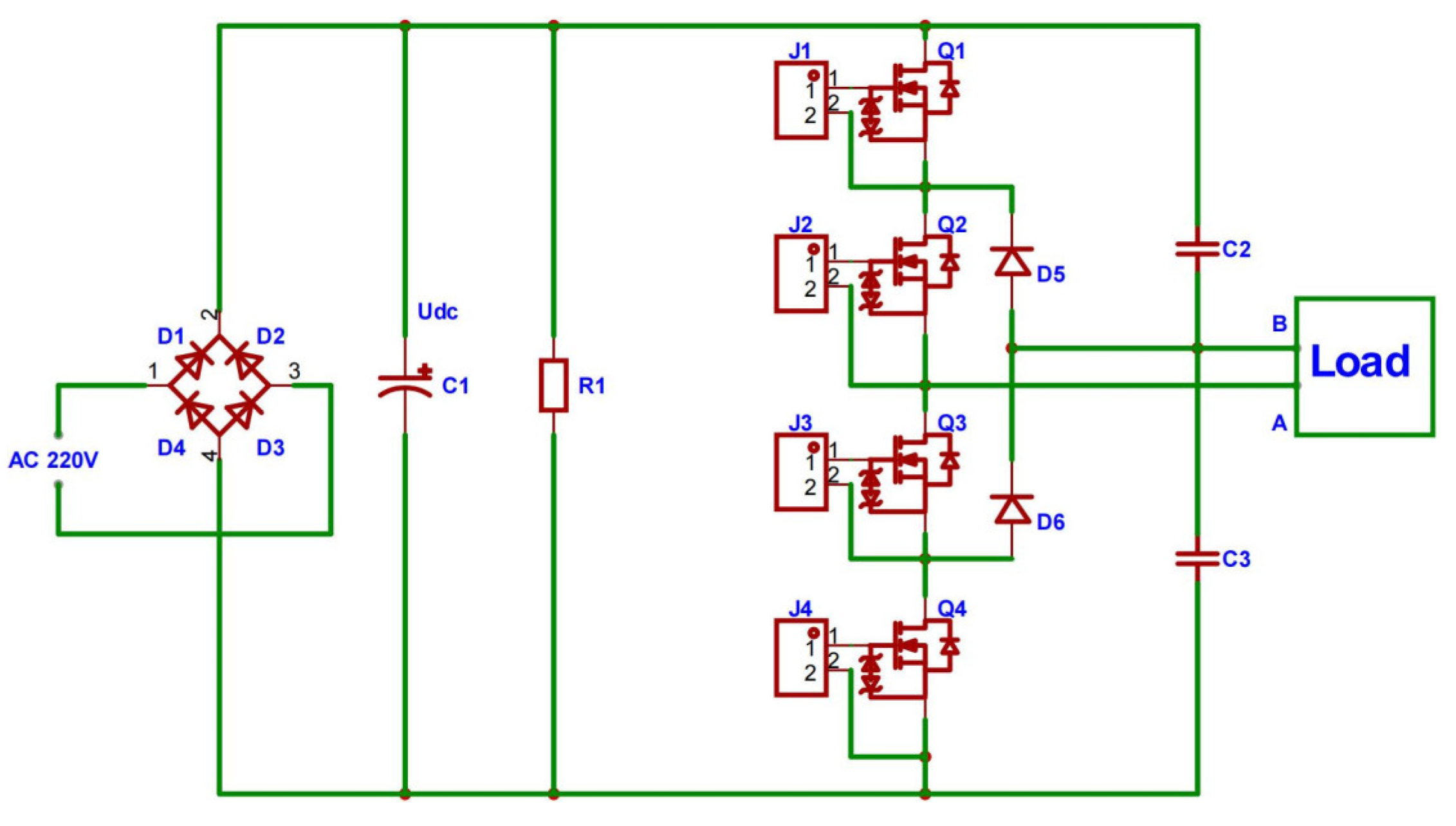
As shown in Figure 2, the main inverter circuit of the design is a diode-clamped NPC three-level inverter [25]. In Figure 2, numbers 1–2 represent the input of the rectifier bridge module, and numbers 3–4 represent the output of the rectifier bridge module. This system adopts a single-phase three-level topology circuit, which has the following two advantages compared to other three-level circuits (such as three-phase three-level or other three-level topologies):
  • Reduction in the number of components and cost reduction:
Compared to three-phase three-level circuits, single-phase three-level circuits have reduced the number of switching devices such as IGBTs, MOSFETs, clamp diodes, and drive circuits, thereby lowering system costs. For example, single-phase NPC circuits typically use four main switches and two clamp diodes, while three-phase NPC circuits require twelve main switches and six clamp diodes;
2.
Overall loss reduction:
Compared to three-phase structures, single-phase structures have relatively lower overall, switching losses and conduction losses. The single-phase three-level topology circuit consists of four power MOSFETs and two clamping diodes, where Q2, Q3, D5, and D6 form a clamping midpoint-type circuit. The output of the controllable rectifier is composed of two support capacitors, C2 and C3, with the midpoint of the capacitors connected to the midpoint of the clamping diode bridge arm [26,27,28,29]. The AC 220 V voltage passes through the bridge rectifier module, producing a DC output voltage of 310 V. The rectifier bridge module used in this experiment is the KBPC5010, with a peak reverse voltage of 1000 V and an average rectified output current I a v of 50 A. Assuming an input voltage of 220 V and a peak output voltage U m a x of approximately 220 2 V, the peak output power P m a x can be calculated using Equation (1), yielding 15.56 kW.
P m a x = U m a x I a v
Therefore, this rectifier bridge module meets the design requirement of 15 kW peak output power.
To accommodate the rectified output power of 15 kW and an output voltage of 220 2 V, the filtering capacitor C1 in Figure 2 is selected with a capacitance of 560 µF and a withstand voltage of 450 V.
SiC MOSFETs are selected for Q1, Q2, Q3, and Q4, and D5 and D6 are SiC diodes.
Points A and B are connected to the load, with the current flowing from point B to point A defined as the positive direction of the load current [30]. The output B to the inverter potential A is U B A [31]. When the switches Q1 and Q2 are on and the switches Q3 and Q4 are off, the output voltage from point B to point A is + U d c 2 ; when the switches Q2 and Q3 are on and the switches Q1 and Q4 are off, the output voltage is 0; when the switches Q3 and Q4 are on [32] and the switches Q1 and Q2 are off [33], the output voltage is U d c 2 . The switching states of the all-SiC NPC three-level inverter are summarized in Table 3 [34,35,36,37]. P denotes the positive voltage + U d c 2 , and N denotes the negative voltage U d c 2 [38].
For convenience, define the ideal switching function S i as follows:
S i = 1   S a = 1 0   S a = 0 1   S a = 1
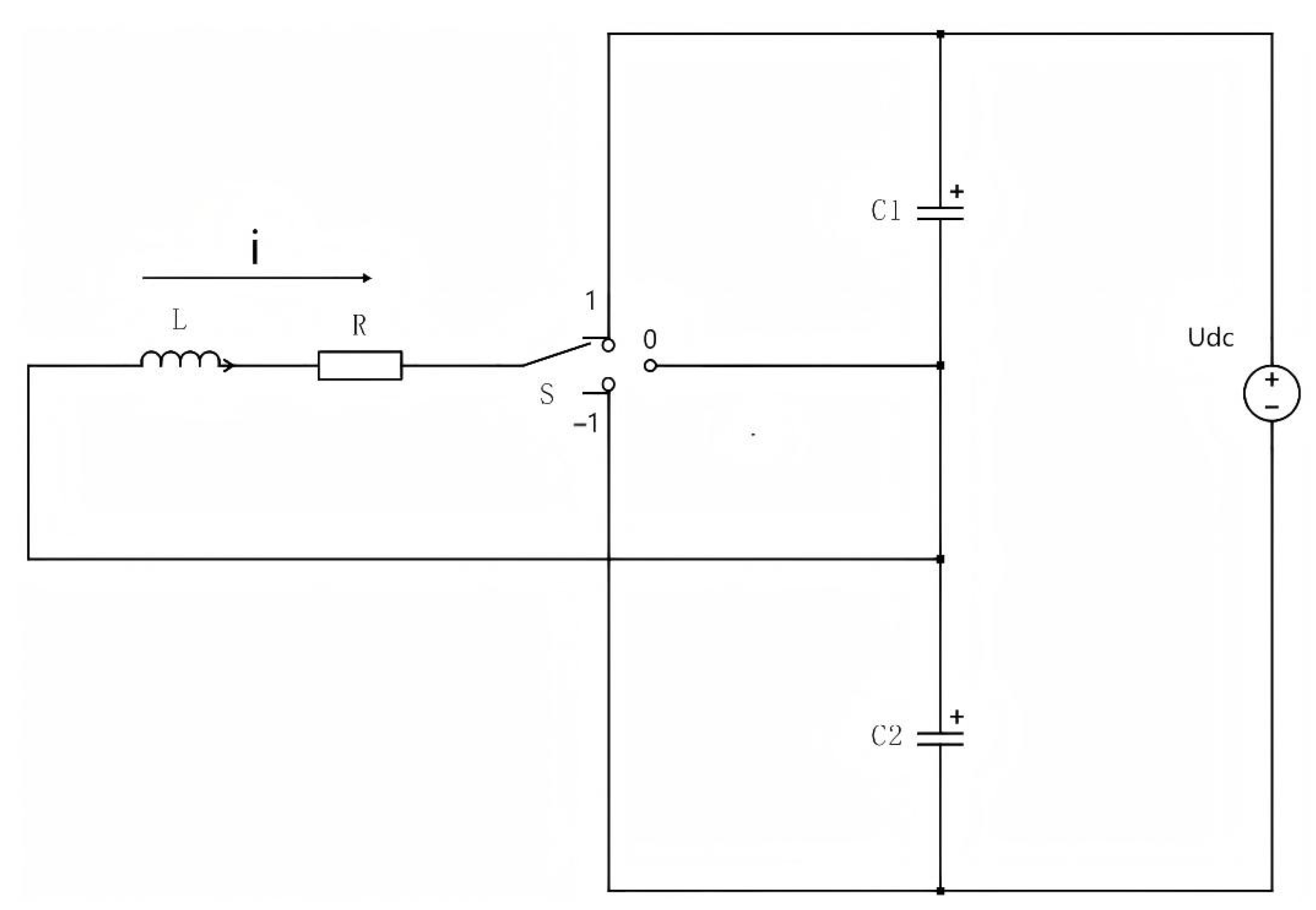
where S a represents the circuit switch status. Based on the ideal switching function S i , the three-level high-frequency inverter main circuit can be represented by the equivalent circuit shown in Figure 3, where R and L are the equivalent loads between points A and B. The bridge arm has three equivalent states: 1, 0, and −1.
Applying KVL’s law to the equivalent circuit shown in Figure 3, we obtain the following [39]:
L d i d t + R i = U C 1 = s U d c 2
Based on the voltage–capacitance relationship of C 1 , C 2 , we derive the equations below:
C 1 d U C 1 d t = 1 2 + s 2 i
C 2 d U C 2 d t = 1 2 s 2 i
where s = 1,0 , 1 .
The mathematical model of the three-level high-frequency inverter main circuit can be expressed as follows [40,41,42]:
d i d t = R L i + s 2 L U d c d U C 1 d t = 1 + s 2 C 1 i d U C 2 d t = 1 s 2 C 2 i
Therefore, the state equation of the three-level high-frequency inverter main circuit is as follows [43]:
d i d t d U C 1 d t d U C 2 d t = R L 0 0 1 + s 2 C 1 0 0 1 s 2 C 2 0 0 i U C 1 U C 2 + s 2 L 0 0 U d c
set up as outlined below:
X ˙ = A X + B U
where
A = R L 0 0 1 + S 2 C 1 0 0 1 S 2 C 2 0 0 ;   X = i U C 1 U C 2 ;   B = S 2 L 0 0 ; U =   U d c
Compared with the two-level structure, the three-level structure has only half of the switching DC voltage with the same bus voltage, which brings a lot of advantages, mainly including the following points:
  • Better output waveform:
In the three-level bridge arm commutation process, each level change is from positive or negative first to the midpoint potential. This process gives an extra step, which is converted to phase voltage, making the step of the waveform change smoother and closer to a sine wave. As a result, a three-level waveform is much smoother than a two-level one. Usually two-level output voltage-harmonic THD (total harmonic distortion) is generally about 50%, while in the case of the same switching frequency, three-level harmonic THD is only about 26%. The reduction is close to about half, which also helps a lot to reduce the harmonic injection into the grid;
2.
Improvement in electromagnetic interference (EMI) problems:
Voltage variation rate ( d v / d t ) is the main source of electromagnetic interference in power electronic systems. In the three-level structure, the switching voltage of the MOSFET switching device is reduced by half. The voltage variation rate ( d v / d t ) reduction means that the system’s electromagnetic interference (EMI) is reduced and improved [44];
3.
Lower loss, higher efficiency, and higher switching frequency:
During the switching process, the reduction in DC voltage for MOSFET turn-on and turn-off significantly reduces the switching loss of the chip. According to empirical data, the relationship between DC voltage and switching loss is given by the following equation [45]:
E S W V d c V r e f 1.3
Calculations show that when the switching DC voltage is reduced to 50%, the losses decrease to approximately 40% of the original value. Lower losses result in higher efficiency and enable higher switching frequencies. In the design of the LC filter, increasing the switching frequency helps reduce the size and volume of the reactor as well as facilitating a more reliable resonance point design.

2.2.1. Selection of Power MOSFETs

When a DC voltage of 310 V is applied to the DC side of the inverter, each power switching tube is subjected to a DC voltage of 155 V due to the clamping effect of the clamping diode. The GC2M0040120D SiC MOSFET (TO-247-3 package) made by Guojing Microelectronics in Wuxi, China was selected for the T-bridge arms, offering a drain-source withstand voltage U D S of 1200 V and a leakage current I D of 55 A. This device provides a 3.9× safety margin relative to the nominal DC bus voltage (310 V), ensuring reliable operation under high-temperature conditions while minimizing switching losses.

2.2.2. Selection of Voltage Divider Capacitors

Under normal operation, each voltage divider capacitor on the DC side of the main circuit is subjected to a voltage of 155 V. To ensure reliability, the rated voltage of the voltage divider capacitor should be at least 310 V, considering a safety margin of 2 times. To minimize the influence of midpoint potential shifts on the test results, the capacitance value of the voltage divider capacitor should be as large as possible [46].
Non-polarized capacitors, such as ceramic or film capacitors, are preferred due to their superior voltage resistance and stability. Additionally, non-polarized capacitors exhibit excellent high-frequency characteristics, making them ideal for use in the NPC diode-clamped three-level inverter.
The size of the voltage divider capacitor in an NPC circuit can be estimated using the following formula. Assuming the voltage divider capacitor C is used in the three-level inverter topology, the basic equation for capacitor sizing is outlined below [47]:
C = I a v 2 π f v
I a v = I P P 2 2
v = u P P × 1 % ~ 2 %
where
  • C is the value of the voltage dividing capacitance (in Farad, F);
  • Iav is the effective value of the busbar current (in Amperes, A);
  • f is the switching frequency (in Hertz, Hz);
  • Δv is the permissible midpoint voltage ripple (in Volts, V), typically 1% to 2% of the bus voltage.
For this design, the peak-to-peak bus current I P P is 45 A, the switching frequency f is 25 kHz, and the bus voltage U P P is 310 V. Using Equations (11)–(13), the required capacitance C is calculated to be 32.69 μF. Therefore, a welding machine capacitor with a rated voltage of 400 V and a capacitance of 35 μF is selected, considering the margin.

2.2.3. Selection of Clamp Diodes

Based on the operating current and maximum-reverse-voltage requirements of the diode in the three-level circuit, the SiC diode model GC4D30120H (TO-247-2 package) made by Guojing Microelectronics in Wuxi, China is selected. This diode has a DC reverse withstand voltage U R R M of 1200 V and a rectifier current I F of 68 A.

2.3. Design of the Three-Level High-Frequency Control Main Circuit

2.3.1. Drive Circuit Design

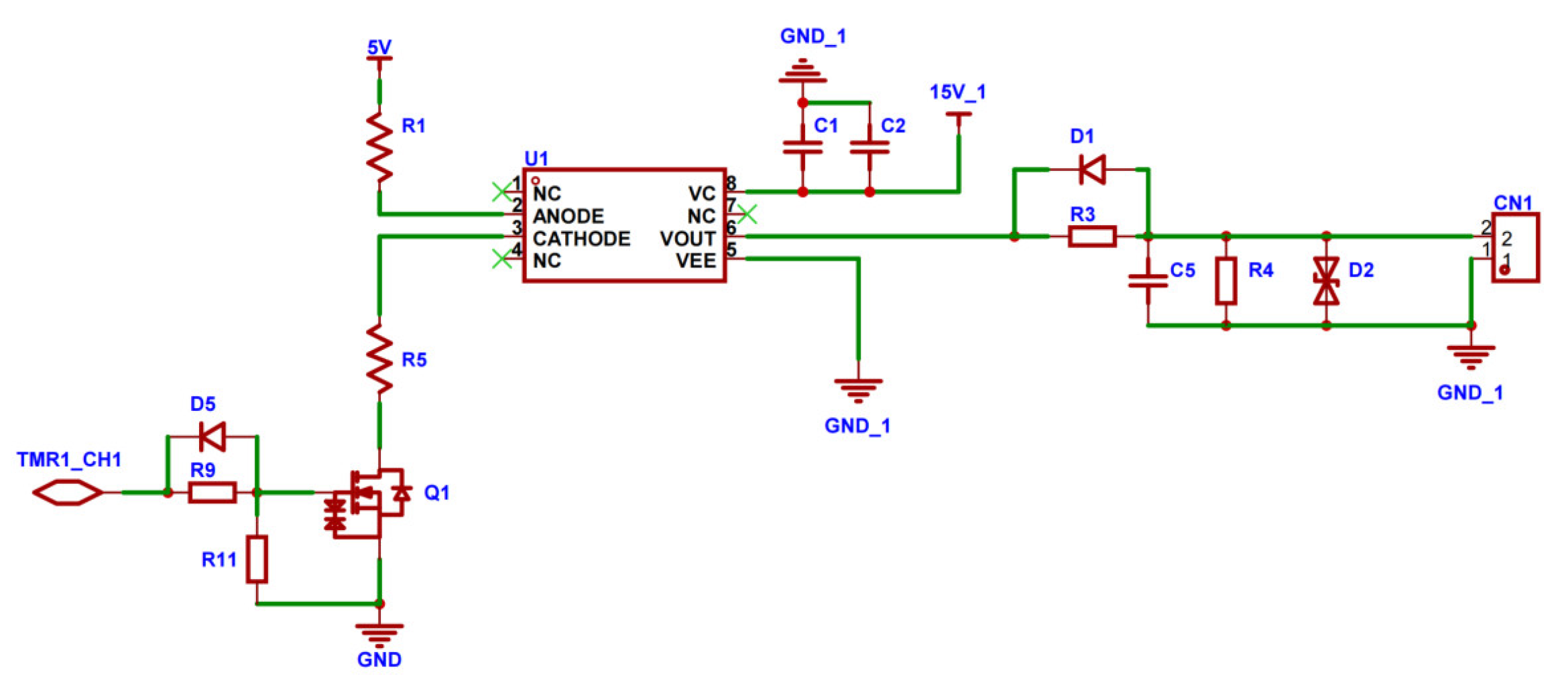
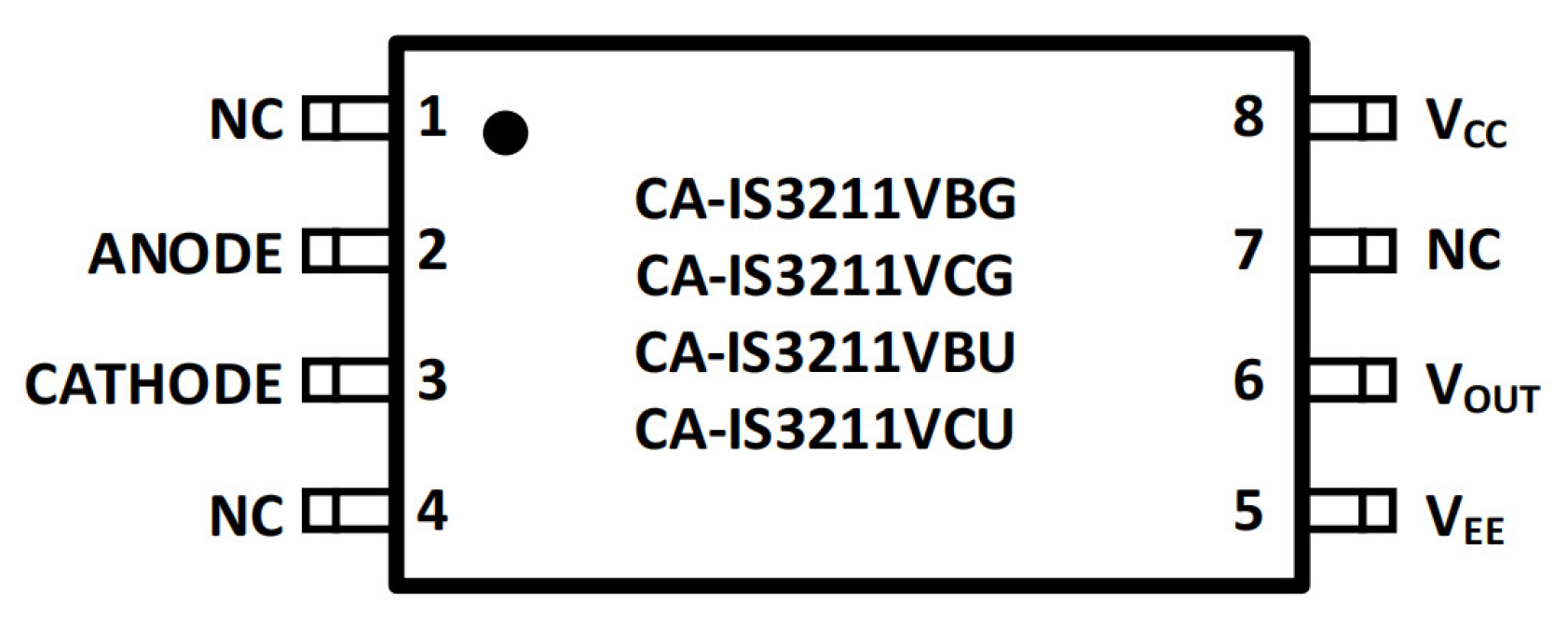
As shown in Figure 4, the schematic diagram of the high-frequency inverter driving circuit uses the CA-IS3211 chip made by Chuantu Micro Manufacturing in Shanghai, China as the main circuit switching tube driver. For the CA-IS3211 chip, pins 1–8 are defined as: 1(NC), 2(ANODE), 3(CATHODE), 4(NC), 5(VEE: negative output stage power rail), 6(VOUT: output), 7(NC), 8(VCC: positive output stage power rail). NC pins remain unconnected. As illustrated in Figure 5, the CA-IS3211 is an optocoupler-compatible single-channel isolated gate driver capable of driving MOSFETs, IGBTs, and SiC devices. With an isolation rating of 5.7 kVRMS, the chip provides a 5 A pull and 6 A injected peak current capability. Conventional PWM drive circuits often face the following issues:
  • Low common-mode transient immunity (CMTI): a low CMTI can lead to false triggering or output switching errors due to transient noise at high switching frequencies;
  • High transmission delay: especially in high-speed switching applications, high transmission delay affects the response speed of the PWM signal;
  • High pulse width distortion: this increases the deviation between the PWM signal pulse width and the ideal value, reducing system performance and reliability.
The driver circuit proposed in this study effectively improves the CMTI, reduces transmission delay, and minimizes pulse width distortion, thereby enhancing the overall performance of the PWM driver circuit. Key components include the following:
  • R11: gate resistor to control gate charging and discharging speed;
  • C2: 15 V power supply filtering capacitor;
  • R3 and R9: current-limiting resistors;
  • C5 and R4: filtering components;
  • D2: TVS tube to protect against instantaneous surge pulse voltages;
  • D1 and D5: continuity diodes to prevent reverse current damage.

2.3.2. Design of the Isolated Power Supply Circuit

The single-phase three-level inverter circuit requires four separate DC power supplies for the four MOSFETs. As shown in Figure 6, the F2415S-2WR2 isolated power module is used, which accepts an input voltage range of 21.6–26.4 V and provides four isolated 15 V outputs to the CA-IS3211 driver chip. Key components are outlined below:
  • C13, C14, and C25: power filtering capacitors;
  • C21: isolation capacitor to isolate the ground of input 24 V from the ground of output 15 V.

2.4. Design of the High-Frequency High-Voltage Transformer

2.4.1. Selection of Transformer Primary Wire

As shown in Table 2, the design specifications for the peak-to-peak value of the bus current I P P in the plasma power supply system is 45 A, and its effective value I a v is calculated as 15.91 A using Formula (12).
The primary output line of the transformer is constructed from multiple strands of wire. Each strand has a diameter r of 0.1 mm, and 400 strands are wound together. The effective current I e flowing through the primary side of the transformer is calculated using the following formula:
I e = 400 π r 2 2 J
where J is the current density of the multiple wires, with a value of 5.5 A / m m 2 . Based on Equation (14), the effective current I e is 17.28 A. To meet the voltage-resistance and heat-dissipation requirements of the plasma power supply system, polyurethane enameled wire is selected for the multi-strand core wire, and polyimide film is used as the outer insulation. This multi-strand wire exhibits excellent insulation, high-voltage resistance, and heat resistance, withstanding temperatures up to 180 °C, ensuring reliable operation in high-temperature environments.

2.4.2. Selection of Transformer Materials

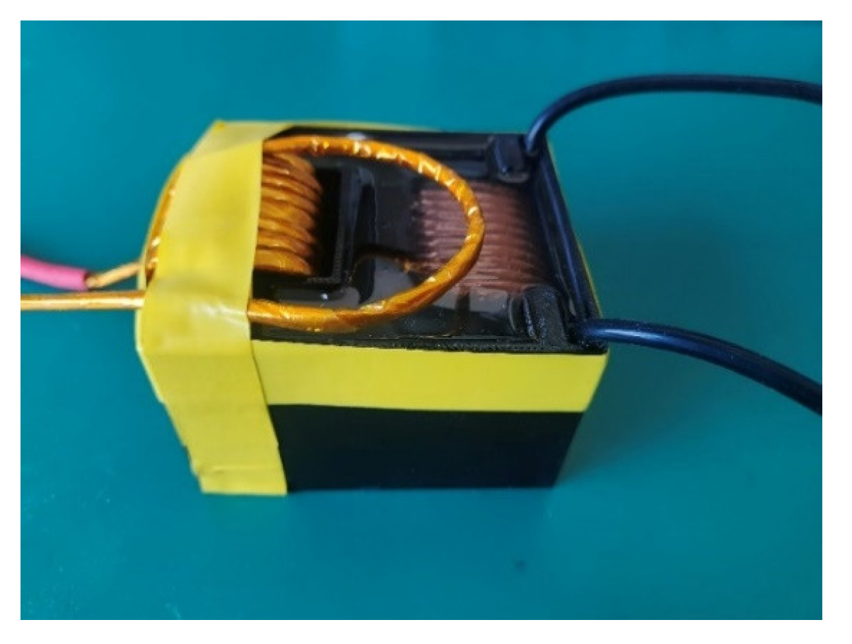
The transformer core is made of ferrite PC40, which operates optimally at a frequency range of 20–40 kHz, with a peak performance at 25 kHz. The secondary output line is constructed from high-voltage silicone wire, capable of withstanding voltages up to 40 kV. The primary output line, as described in Section 2.4.1, is made of high-temperature and high-voltage-resistant multi-strand wire. The designed UY16 ferrite transformer, shown in Figure 7, meets the design requirements for a plasma power system with a peak-to-peak bus current of 45 A, a load voltage of 25 kV, an operating frequency of 25 kHz, and high-temperature resistance.

2.5. Device of the High-Frequency High-Voltage Plasma Power Supply System

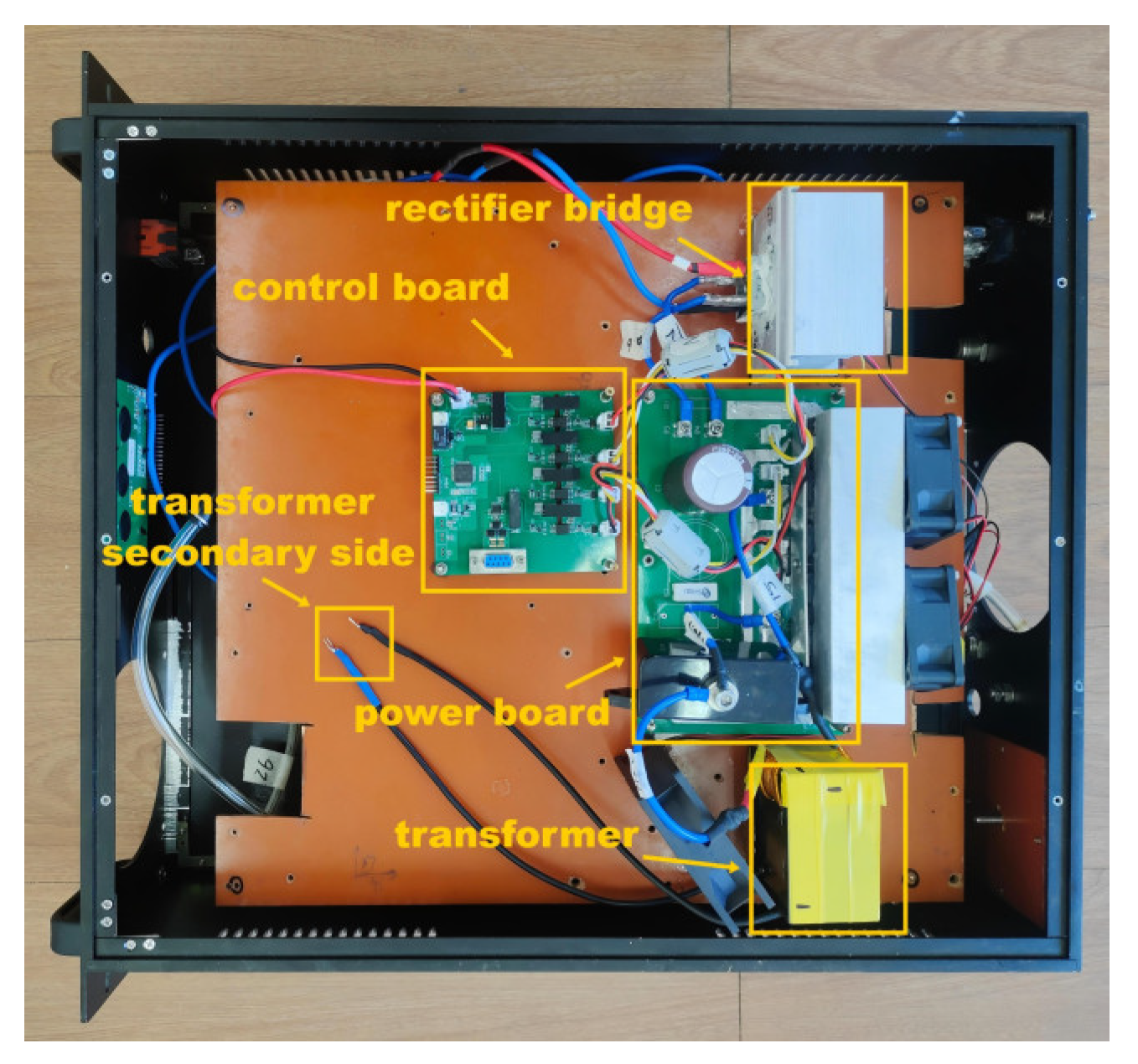
Figure 8 shows a plasma power supply system utilizing all-SiC power devices, which is mainly composed of a rectifier bridge module, the control board of a three-level high-frequency control main circuit, the power board of a three-level high-frequency inverter main circuit, and a ferrite high-frequency transformer of type UV16.

2.6. Discussion of PWM Control Strategies

In three-level driving circuits, neutral-point potential balancing requires careful consideration. Neutral-point potential deviation may induce the following adverse effects:
  • Uneven voltage distribution in DC-link capacitors, resulting in excessive voltage stress on power devices (e.g., MOSFETs or diodes) beyond their rated thresholds. This accelerates device degradation and risks dielectric breakdown failures;
  • Output voltage distortion, which elevates total harmonic distortion (THD) and compromises power quality;
  • Additional charge–discharge losses, degrading overall system efficiency.
To address these challenges, appropriate PWM control strategies are adopted in this design to stabilize the neutral-point potential. Table 4 introduces several common PWM control strategies. In this study, a symmetric complementary PWM control strategy is adopted to achieve neutral-point potential balancing by regulating the switching states of the all-silicon NPC three-level inverter, as detailed in Table 3.

3. Results and Discussion

3.1. Analysis of PWM Drive Signal Source

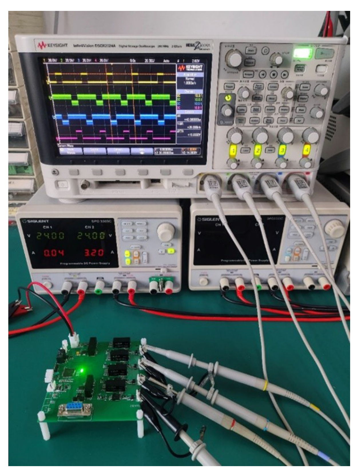
In this experiment, the model DSOX2024A Keysight oscilloscope made by headquarters located in Santa Rosa, CA, USA and the model SPD3303C Siglent programmable DC power supply made by Siglent Technology in Shenzhen, China were used to test and analyze the PWM drive signal. Figure 9 shows an experimental diagram of the PWM drive signal source generated by the high-frequency control main circuit.
As shown in Figure 10 for the PWM drive signal, the experiment utilizes AT32 to output four PWM waveforms with a frequency of 25 kHz, adjustable duty cycles, and fixed phase shifts.
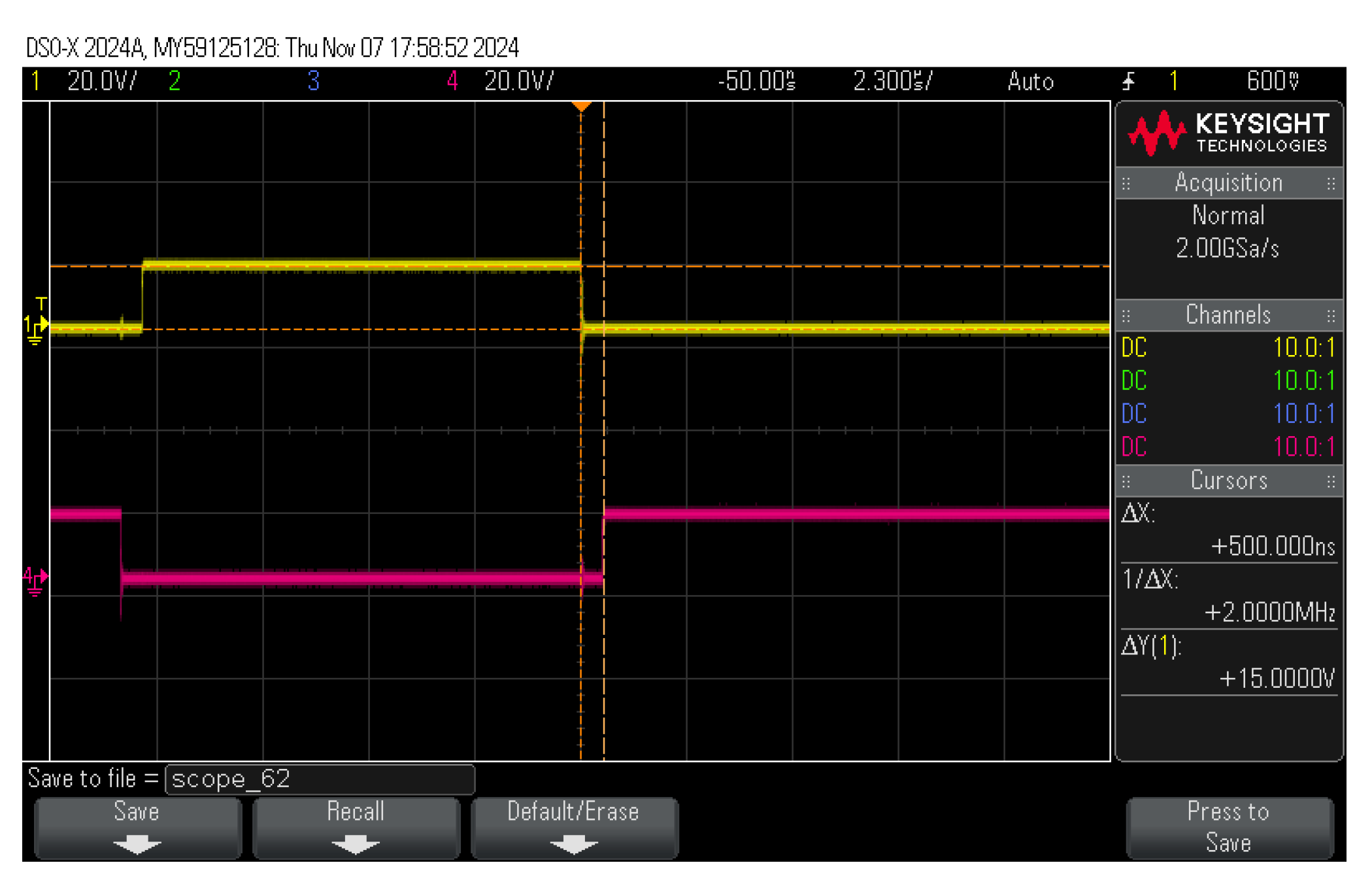
Using manual measurement method, as illustrated in Figure 11, to mitigate the risk of shoot-through in the bridge arm and prevent MOSFET damage, a dead time of 500 ns was implemented between complementary signals (Q1–Q3 and Q2–Q4), effectively reducing MOSFET heat generation and temperature rise.

3.2. Analysis of Three-Level Voltage Signal

As shown in Figure 12, using manual measurement method, the peak-to-peak busbar voltage U P P P is 312 V, which meets the design requirements.
As shown in Figure 13, using manual measurement method, the upper half-peak voltage is 156 V. The lower half-peak voltage is also 156 V. The same value for the upper and lower half-peak voltages indicates a midpoint potential balance. The experimental results have shown that a symmetric complementary PWM control strategy can achieve midpoint potential balance and ensure stable voltage waveform output by the inverter. Midpoint potential balancing reduces the voltage stress on the capacitor and extends the life of the capacitor. At the same time, it can reduce the voltage stress of the inverter switching tube and improve the reliability of the system.

3.3. Analysis of Three-Level Current Signal

As shown in Figure 14, using manual measurement method, the peak-to-peak bus current I P P P is 43 A, which complies with the design specifications.
As shown in Figure 15, using manual measurement method, the upper half-peak current is 21.5 A. Symmetrical upper and lower half-peak currents of 21.5 A further validate the system stability.

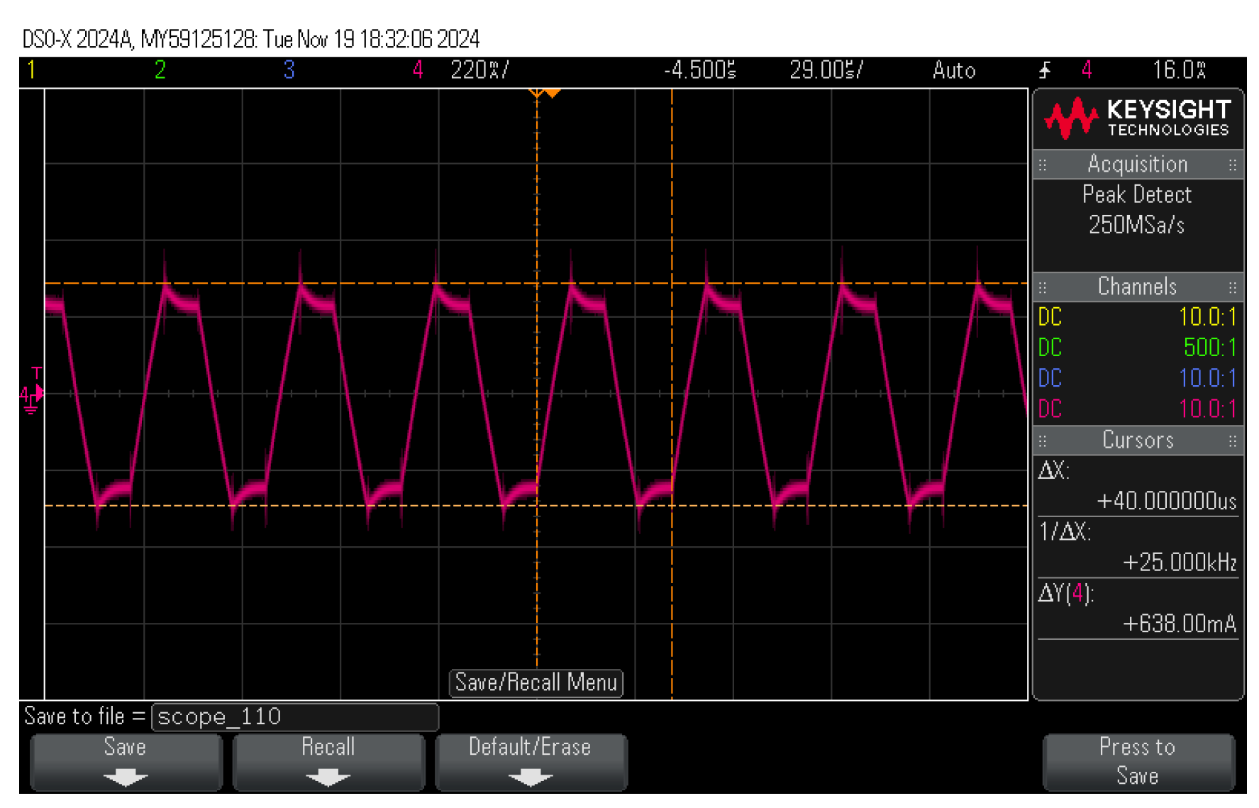
3.4. Analysis of Transformer Output Signal

As shown in Figure 16, using manual measurement method, the peak value of the transformer’s secondary current I P P S is 0.638 A, and the peak value of the bus current I P P P is 43 A, as discussed earlier in Figure 14. Also, the peak value of the bus voltage U P P P is 312 V, as discussed earlier in Figure 12. Therefore, the peak-to-peak value of the secondary voltage U P P S can be calculated by Equations (15) and (16), which equals 21.03 kV.
N = I P P P I P P S
U P P S U P P P = I P P P I P P S
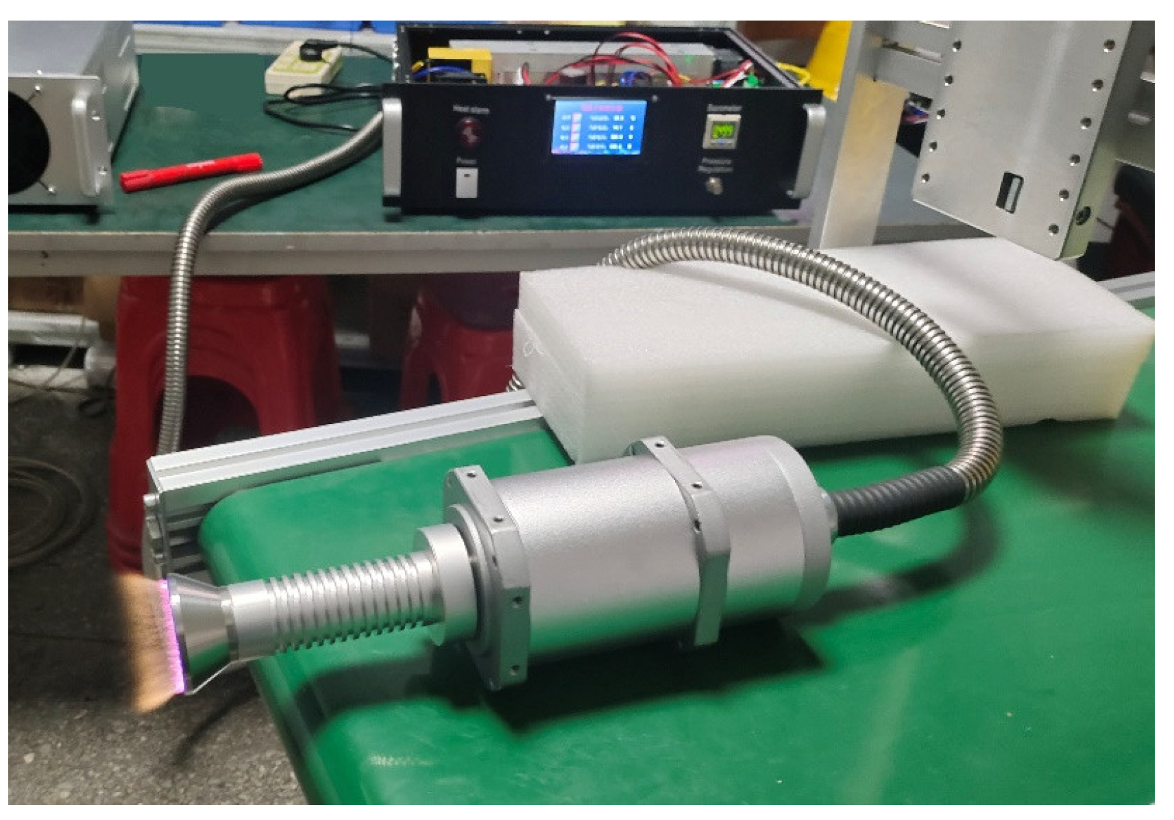
After connecting the rotary gun, the plasma flame profile of the rotary gun is shown in Figure 17. The flame pattern is stable and homogeneous, which means that the plasma density and temperature distribution are uniform throughout the flame region.
The operational parameters are presented in Figure 18. Through serial communication, the power output is measured at 13.42 kW, with a bus current of 43 A and a bus voltage of 312 V. Furthermore, the system maintains a stable operating temperature of approximately 28 °C.
Table 5 presents the operational performance data of the plasma power supply system under high-frequency and high-voltage conditions. The system was tested at ambient temperature for a duration of 8 days, with continuous daily operation of 10 h, accumulating a total of 80 operational hours.
The plasma power supply system demonstrates exceptional thermal stability during prolonged operation, primarily attributed to the implementation of SiC MOSFETs as the driving components. This enhanced performance stems from the superior material properties of silicon carbide, which exhibits a thermal conductivity exceeding twice that of conventional silicon. Furthermore, SiC demonstrates significantly improved heat dissipation characteristics compared to Si-based components. Consequently, the SiC-based plasma power supply system maintains stable thermal conditions during extended high-frequency, high-voltage operations, thereby ensuring optimal system reliability.

4. Conclusions

In this study, a high-performance plasma power supply system is developed by integrating the superior output voltage quality of a three-level inverter with the advanced characteristics of third-generation semiconductor materials. The system demonstrates exceptional stability under high-frequency and high-voltage conditions, achieving a consistent power output of 13.42 kW at 25 kHz with an output voltage of 21.03 kV. Experimental observations confirm uniform plasma density and temperature distribution, as evidenced by the stable and homogeneous flame pattern. Over an 8-day operational period, the system maintained normal operating temperatures without any heating issues, highlighting its reliability and extended lifespan. This innovative design effectively mitigates the challenges of voltage instability and thermal degradation in high-frequency environments, achieving a stable power output of 13.42 kW while significantly improving system reliability and operational lifespan. By combining the multilevel output capabilities of a three-level inverter with the high-frequency and high-voltage properties of SiC, the system enables efficient plasma generation. Despite its advantages, the system faces certain challenges, as outlined below:
  • High device cost: SiC devices are more expensive to manufacture compared to traditional silicon-based components, resulting in higher overall system costs. Although technological advancements and mass production have reduced costs, SiC-based solutions remain more expensive than their silicon counterparts;
  • Complex control strategy: the three-level topology requires a more sophisticated control strategy to ensure precise switching device operation and output voltage stability. This complexity increases the difficulty of control system design.
The high-frequency high-voltage plasma power supply system presented in this study offers valuable insights for research and development in fields such as material modification, chemical synthesis, metallurgical refining, and optical material purification. Despite the aforementioned challenges, ongoing advancements in three-level drive control technology and the decreasing cost of silicon carbide are expected to drive the widespread adoption of all-SiC high-frequency high-voltage plasma power supply systems across diverse applications.

Author Contributions

Conceptualization, J.X. and K.C.; methodology, J.X. and K.C.; software, Z.Y. and R.H.; validation, K.C. and Z.Y.; formal analysis, Z.Y. and R.H.; investigation, K.C. and Z.Y.; resources, J.X. and K.C.; data curation, K.C. and Z.Y.; writing—original draft preparation, K.C.; writing—review and editing, J.X. and K.C.; visualization, Z.Y. and R.H.; supervision, J.X. and K.C.; project administration, J.X. and K.C.; funding acquisition, J.X. All authors have read and agreed to the published version of the manuscript.

Funding

This research was supported by the National Natural Science Foundation of China (62164004) and the Plasma Generator Technology Development Project (CD24181X).

Data Availability Statement

Additional data are available upon request by contacting the corresponding author of this manuscript.

Conflicts of Interest

The authors declare that there are no conflicts of interest regarding the publication of this paper.

References

  1. Wang, Z.M.; Fan, W.Y.; Xie, F.X.; Ye, C.X. An 8kW LLC resonant converter in plasma power supplybased on SiC power devices for efficiency improvement. Circuit World 2019, 45, 181–188. [Google Scholar]
  2. Rong, J.; Ai, X.; Li, Y.; Ren, D. Research on the structure and control strategy of a novel power electronic transformer for AC/DC hybrid distribution network. Appl. Sci. 2019, 9, 727. [Google Scholar] [CrossRef]
  3. Safder, M.U.; Rizvi, S.T.; Meng, Y.; Javed, M.Y.; Jaffery, M.H.; Hassan, M.S. Low-frequency ac power transmission and distribution for subsea application using hexverter. Electronics 2020, 9, 61. [Google Scholar] [CrossRef]
  4. Jiang, D.Z.; Zhang, Z.H. Control strategy of three-phase H-bridge cascaded static synchronous compensator. High-Volt. Technol. 2011, 37, 2024–2032. [Google Scholar]
  5. Nabae, A.; Takahashi, I.; Akagi, H. A new neutral-point-clamped PWM inverter. IEEE Trans. Ind. Appl. 1981, 5, 518–523. [Google Scholar]
  6. Chang, F.; Zhao, L.P.; Feng, J.B. Application of five-level AC-DC converter in through-phase power supply. Power Syst. Its Self J. Anim. Chem. 2015, 27, 26–31. [Google Scholar]
  7. Beig, A.R.; Dekka, A. Experimental verification of multilevel inverter-based standalone power supply for low-voltage and low-power applications. IET Power Electron. 2012, 5, 635–643. [Google Scholar]
  8. Sadikin, M.; Senjyu, T.; Yona, A. DC–DC type high-frequency link DC for improved power quality of cascaded multilevel inverter. Int. J. Emerg. Electr. Power Syst. 2013, 14, 333–340. [Google Scholar] [CrossRef]
  9. Han, D.; Li, S.; Lee, W.; Sarlioglu, B. Adoption of wide bandgap technology in hybrid/electric vehicles-opportdeviceies and challenges. In Proceedings of the 2017 IEEE Transportation Electrification Conference and Expo (ITEC), Chicago, IL, USA, 22 June 2017; IEEE: New York, NY, USA, 2017; pp. 561–566. [Google Scholar]
  10. Ma, B. Comparative study on the performance of inverter systems based on Si and SiC devices. Electr. Drives 2017, 47, 3–6. [Google Scholar]
  11. Sheng, Z.; Dong, Z.Z.; Wu, X.K. Review and outlook of key technologies for silicon carbide power device packaging. Chin. J. Electr. Eng. 2019, 39, 5576–5584. [Google Scholar]
  12. Krisna, T.N.; Sathishkumar, P.; Himasree, P.; Punnoose, D.; Raghavendra, K.V.; Himanshu; Naresh, B.; Rana, R.A.; Kim, H.J. 4T analog MOS control-high-voltage high-frequency (HVHF) plasma switching power supply for water purification in industrial applications. Electronics 2018, 7, 245. [Google Scholar] [CrossRef]
  13. Neretti, G.; Ricco, M. Self-tuning high-voltage and high-frequency sinusoidal power supply for dielectric barrier discharge plasma generation. Electronics 2019, 8, 1137. [Google Scholar] [CrossRef]
  14. Cai, X.W.; Fu, Z.H.; Xie, H.S.; Xue, J.X.; Ding, D.H.; Ou, N.; Zhou, G. Resonant Power Supply for Plasma Cleaning Based on Fuzzy Logic Power Tracking. Appl. Sci. 2022, 12, 4681. [Google Scholar] [CrossRef]
  15. Krupski, P.; Stryczewska, H.D. The Investigation of the Properties of High-voltage Transformer in Nonthermal Plasma Pulse Power Supply. In Proceedings of the 2018 14th Selected Issues of Electrical Engineering and Electronics (WZEE), Szczecin, Poland, 19 November 2018; IEEE: New York, NY, USA, 2018; pp. 1–4. [Google Scholar]
  16. Xun, Q.; Xun, B.; Li, Z.; Wang, P.; Cai, Z. Application of SiC power electronic devices in secondary power source for aircraft. Renew. Sustain. Energy Rev. 2017, 70, 1336–1342. [Google Scholar]
  17. Han, G.J.; Deng, J.L.; Xu, D. Research on high-frequency and high-voltage switching power supply for electrostatic precipitator. Appl. Mech. Mater. 2013, 241, 653–656. [Google Scholar] [CrossRef]
  18. Zhao, Z.Q.; Wang, Z. Designing and Simulation Testing of Kilowatt Switching Power Supply Transformer. Adv. Mater. Res. 2012, 490, 1332–1336. [Google Scholar]
  19. Li, P. Design and Research of Medical Plasma Power Supply; Chang’an University: Xi’an, China, 2022. [Google Scholar] [CrossRef]
  20. Zhu, W.; Wu, S.B.; Lu, H.Y.; Hong, X.; Yu, J.J.; Zhang, Y. The design of high-voltage direct current power supply for the electrical fast transient pulse/burst generator. Appl. Mech. Mater. 2014, 494, 1452–1456. [Google Scholar]
  21. Sato, K.; Sato, T.; Sonehara, M.; Takeuchi, H. Low permeability composite magnetic core transformer with high coupling coefficient and its application to PFM controlled quasi-resonant mode flyback-type DC-DC converter. J. Magn. Soc. Jpn. 2017, 41, 132–139. [Google Scholar]
  22. Seo, H.; Kwon, H.; Kwon, Y.; Kim, K.; Choi, S.; Kim, H.; Jang, K. Fast number theoretic transform for ring-LWE on 8-bit AVR embedded processor. Sensors 2020, 20, 2039. [Google Scholar] [CrossRef]
  23. Li, G.J. Design of Intelligent Control of DC Motor. Appl. Mech. Mater. 2013, 313, 427–431. [Google Scholar]
  24. Bai, X.F.; Li, P.; Li, H.; Song, X.N.; Wang, C.W. The Vertical Axis Wind Power Controller Design. Adv. Mater. Res. 2013, 816, 989–992. [Google Scholar]
  25. Yang, G.; Fu, C.; Yi, H.; Chai, C.; Huang, B.; Hao, S.; Chen, Z. Direct power control of three-level NPC grid-connected system combined with fault-tolerant technology. Microelectron. Reliab. 2018, 88, 1057–1062. [Google Scholar]
  26. Rukin, S.N. Pulsed power technology based on semiconductor opening switches: A review. Rev. Sci. Instrum. 2020, 91, 011501. [Google Scholar] [CrossRef]
  27. Syed, A.; Sandipamu, T.K.; Suan, F.T. High-efficiency neutral-point-clamped transformerless MOSFET inverter for photovoltaic applications. IET Power Electron. 2018, 11, 246–252. [Google Scholar]
  28. Lu, T.; Zhao, Z.; Yu, H.; Ji, S.; Yuan, L.; He, F. Parameter design of a three-level converter based on series-connected HV-IGBTs. IEEE Trans. Ind. Appl. 2014, 50, 3943–3954. [Google Scholar]
  29. Rajalakshmi, S.; Rangarajan, P. Investigation of modified multilevel inverter topology for PV system. Microprocess. Microsyst. 2019, 71, 102870. [Google Scholar]
  30. Li, M.; Jia, K.; Bi, T.; Wang, C.; Zhu, R.; Yang, Q. Full-current-based directional pilot protection for VSC-DC distribution systems. IET Gener. Transm. Distrib. 2019, 13, 3713–3724. [Google Scholar]
  31. Islam, M.; Mekhilef, S.; Hasan, M. Single phase transformerless inverter topologies for grid-tied photovoltaic system: A review. Renew. Sustain. Energy Rev. 2015, 45, 69–86. [Google Scholar]
  32. Chen, H.C.; Lin, R.S. Design of an H-bridge driver without dead-time generation using gate bias. IEICE Electron. Express 2013, 10, 20130656. [Google Scholar]
  33. Liu, G.; Wang, K.; Qu, C.; Liu, S.; Jia, Q.; Li, Y. Phase-shift full bridge power supply based on SiC devices. J. Eng. 2018, 2018, 453–460. [Google Scholar]
  34. Lyu, J.; Hu, W.; Wu, F.; Yao, K.; Wu, J. Three-level saddle space vector pulse width modulation strategy based on two-level space vector pulse width modulation for neutral-point-clamped three-level inverters. IET Power Electron. 2016, 9, 874–882. [Google Scholar] [CrossRef]
  35. Choi, U.M.; Lee, K.B. Space vector modulation strategy for neutral-point voltage balancing in three-level inverter systems. IET Power Electron. 2013, 6, 1390–1398. [Google Scholar] [CrossRef]
  36. Xu, S.Z.; He, F.Y. Improvement of High-Power Three-Level Explosion-Proof Inverters Using Soft Switching Control Based on Optimized Power-Loss Algorithm. J. Electr. Comput. Eng. 2015, 2015, 571209. [Google Scholar] [CrossRef]
  37. Orfanoudakis, G.I.; Yuratich, M.A.; Sharkh, S.M. Analysis of dc-link capacitor current in three-level neutral point clamped and cascaded H-bridge inverters. IET Power Electron. 2013, 6, 1376–1389. [Google Scholar] [CrossRef]
  38. König, N.; Nienhaus, M. A solution to ambiguities in position estimation for solenoid actuators by exploiting eddy current variations. Sensors 2020, 20, 3441. [Google Scholar] [CrossRef]
  39. Rana, N.; Kumar, M.; Ghosh, A.; Banerjee, S. A novel interleaved tri-state boost converter with lower ripple and improved dynamic response. IEEE Trans. Ind. Electron. 2017, 65, 5456–5465. [Google Scholar] [CrossRef]
  40. Phankong, N.; Yuktanon, N.; Bhumkittipich, K. Three-level back-to-back converter simulation for wind turbine energy source. Energy Procedia 2013, 34, 449–458. [Google Scholar] [CrossRef]
  41. Dong, R.; Liu, S.; Liang, G. Research on control parameters for voltage source inverter output controllers of micro-grids based on the fruit fly optimization algorithm. Appl. Sci. 2019, 9, 1327. [Google Scholar] [CrossRef]
  42. Hu, X.; Nan, G. Research of Full Digit Single-phase Inversion Power Supply Based on DSP. Energy Procedia 2012, 17, 580–587. [Google Scholar] [CrossRef]
  43. Liang, C.; Tian, E.; Pang, B.; Li, J.; Yang, Y. Model Predictive Control of LCL Three-level Photovoltaic Grid-connected Inverter. In IOP Conference Series: Earth and Environmental Science; IOP Publishing: Bristol, UK, 2018; Volume 153, p. 042023. [Google Scholar]
  44. Liu, D.; Deng, F.; Chen, Z. Five-level active-neutral-point-clamped DC/DC converter for medium-voltage DC grids. IEEE Trans. Power Electron. 2016, 32, 3402–3412. [Google Scholar] [CrossRef]
  45. Erickson, R.W.; Maksimovic, D. Fundamentals of Power Electronics; Springer Science & Business Media: Berlin/Heidelberg, Germany, 2007. [Google Scholar]
  46. Chen, G.; Zhu, M.; Cai, X. Parameter optimization of the LC filters based on multiple impact factors for cascaded H-bridge dynamic voltage restorers. J. Power Electron. 2014, 14, 165–174. [Google Scholar] [CrossRef]
  47. Mohan, N.; Undeland, T.M.; Robbins, W.P. Power Electronics: Converters, Applications, and Design; John Wiley & Sons: Hoboken, NJ, USA, 2003. [Google Scholar]
Figure 1. Block diagram of high-frequency high-voltage plasma power supply hardware system.
Energies 18 01617 g001
Figure 2. Operating principle of the diode-clamped three-level high-frequency inverter main circuit.
Energies 18 01617 g002
Figure 3. Equivalent circuit of the three-level high-frequency inverter main circuit.
Energies 18 01617 g003
Figure 4. Schematic diagram of the high-frequency inverter driving circuit.
Energies 18 01617 g004
Figure 5. CA-IS3211 chip pinout diagram.
Energies 18 01617 g005
Figure 6. Schematic diagram of the isolated power supply circuit.
Energies 18 01617 g006
Figure 7. Ferrite transformer of the UY16 type.
Energies 18 01617 g007
Figure 8. Plasma power supply system utilizing all-SiC power devices.
Energies 18 01617 g008
Figure 9. Experimental diagram of the PWM drive signal source.
Energies 18 01617 g009
Figure 10. PWM drive signal source.
Energies 18 01617 g010
Figure 11. Schematic diagram of dead-time control in complementary PWM signals.
Energies 18 01617 g011
Figure 12. Peak-to-peak busbar voltage signal.
Energies 18 01617 g012
Figure 13. Upper and lower half-peak voltage signals.
Energies 18 01617 g013
Figure 14. Peak-to-peak busbar current signal.
Energies 18 01617 g014
Figure 15. Upper and lower half-peak current signals.
Energies 18 01617 g015
Figure 16. Secondary current signal of the transformer.
Energies 18 01617 g016
Figure 17. Plasma flame profile of the rotary gun.
Energies 18 01617 g017
Figure 18. The operational status display interface of the plasma power supply system.
Energies 18 01617 g018
Table 1. Typical research status of high-frequency high-voltage plasma power supply systems.
Research InstitutionMethodFrequencyOutput VoltagePower
Pusan National UniversityFull-bridge inverter utilizing silicon-based MOSFETs25 kHz10 kV5 kW
University of BolognaHalf-bridge inverter
utilizing silicon-based MOSFETs
10–60 kHz20 kV200 W
Longyan
University
Phase-shifted full-bridge inverter20–50 kHz3.2 kV500–1000 W
Lublin
University of Technology
Half-bridge inverter utilizing IGBTs10–25 kHz14 kV/
Table 2. Design specifications of the high-frequency high-voltage plasma power supply system.
ParametersPeak-to-Peak Specifications
Busbar   current   I P P 45 A
Busbar   voltage   U P P 320 V
Load   voltage   U 25 kV
Load   power   P 15 kW
Frequency   F 25 kHz
Table 3. Switching states of the all-SiC NPC three-level inverter.
Switching StateQ1Q2Q3Q4 Output   Voltage   U B A
P1100 + U d c 2
001100
N0011 U d c 2
001100
Table 4. Comparison of three common PWM control strategies.
CategoryPrincipleAlgorithm ComplexityApplication Scenarios
Symmetric complementary PWMNeutral-point current charge/discharge magnitudes are balanced between positive/negative half-cycles.LowSimple topologies
SPWM (sinusoidal PWM)PWM waveforms equivalent to sinusoidal signals are generated by comparing sinusoidal reference waves with triangular carrier waves. ModerateUniversal applications
SVPWM
(space vector PWM)
Neutral-point balance is achieved by controlling the duty cycles of redundant small vectors.HighHigh-precision and highly dynamic responses
Table 5. Operational performance parameters of the plasma power supply system.
DaysFrequencyBus VoltageBus Current Power Temperature
225 kHz311.9 V42.9 A13.38 kW27.9 °C
425 kHz312.1 V42.7 A13.33 kW28.1 °C
625 kHz311.2 V43.1 A13.41 kW27.8 °C
825 kHz312.0 V43.0 A 13.42 kW28.0 °C
Disclaimer/Publisher’s Note: The statements, opinions and data contained in all publications are solely those of the individual author(s) and contributor(s) and not of MDPI and/or the editor(s). MDPI and/or the editor(s) disclaim responsibility for any injury to people or property resulting from any ideas, methods, instructions or products referred to in the content.