Article

On the Implementation of “Dead Time” in a Synchronous Step-Down Converter

by
Hristo Antchev
1,* and
Dimitar Borisov
2
1
Department of Metallurgical Technologies, Electrical Engineering and Electronics, University of Chemical Technology and Metallurgy, Kliment Ohridski Blvd., 8, 1000 Sofia, Bulgaria
2
Department of Environmental Engineering, University of Chemical Technology and Metallurgy, Kliment Ohridski Blvd., 8, 1000 Sofia, Bulgaria
*
Author to whom correspondence should be addressed.
Energies 2025, 18(5), 1095; https://doi.org/10.3390/en18051095
Submission received: 24 January 2025 / Revised: 15 February 2025 / Accepted: 21 February 2025 / Published: 24 February 2025
(This article belongs to the Section F3: Power Electronics)

Abstract

:
The paper investigates and addresses the “dead time” of a synchronous step-down converter implemented with P-channel and N-channel transistors. The transistors are controlled by a single driver, and “dead time” is implemented with external circuits and Schottky diodes. The influence of the Schottky diode capacitance on “dead time” is considered. Mathematical expressions were derived, showing the ratio of the value of this capacitance to the input capacitance of the transistor and the influence of this ratio on the shape of the leading edge of the pulse for switching on the transistor. The results of computer simulations are given for different ratios of the two capacitances. It was found that the capacitance of the Schottky diode must be much lower than the input capacitance of the transistor. The results of the mathematical description and computer simulations were used to select a suitable transistor and Schottky diode and are applied in the subsequent practical implementation. Conclusions and recommendations were made for a synchronous step-down converter, as well as for other cases of implementing “dead time” in the manner considered.

1. Introduction

The main issues in the design of DC/DC converters are presented in [1]. The difference between the continuous and discontinuous current modes through the inductance is discussed, for example, in [2]. Typically, a synchronous step-down converter is implemented with two N-channel MOSFETs [3]. Issues related to the efficiency of such a converter are considered, for example, in [4,5,6,7]. The requirements for controlling MOSFETs are considered in many scientific works, such as [8,9,10,11,12]. In cases where the supply voltage does not exceed the maximum allowable gate-source voltage of a P-channel MOSFET, the upper N-channel transistor in a synchronous buck converter can be replaced by a P-channel transistor. This provides certain advantages in terms of controlling both transistors. It can be implemented by a single driver with a push–pull output, as shown in Figure 1. In this way, some additional elements needed to provide the control voltage of the upper transistor in case it is also N-channel—such as a capacitor, diode, and additional circuits—are avoided [13]. However, it should be noted that in the proposed control in Figure 1, one of the two transistors is always on, while in the case of two N-channel transistors, both can be turned off under certain circumstances. This is a known disadvantage of the variant considered in this study, which is suitable, for example, when charging low-power energy storage elements—batteries and ultracapacitors. In this case, constant current regulation and voltage limitation can be carried out, and when the maximum charging voltage is reached, the electronic regulator for this voltage remains operational, i.e., both transistors can be switched. Issues related to regulation and the rest of the control system are not the subject of consideration in this research. The charging circuits of the input capacitances of the two transistors are presented in Figure 1 (red lines) and the discharge circuits (blue lines). The additional elements to the gates of the transistors (the two resistors and the Schottky diode) are known and often recommended. Through these circuits, the so-called “dead time” is implemented when controlling the transistors. The goal is to turn one transistor on with a certain delay compared to turning the other off. This problem is known and also exists in other converters using phase leg transistors [14]. Different methods for implementing “dead time” are known [15,16,17,18,19,20]. For the circuit of a synchronous converter using two N-channel MOSFETs, controllers in an integrated circuit are proposed, with different methods for “dead time” implementation [21,22,23,24]. The proposed drivers with built-in “dead time” implementation are characterized by higher accuracy compared to the circuit considered in the article. However, they cannot be used at low supply voltages, such as for the needs of the present application.
The present work focuses on the implementation with the circuits shown in Figure 1. The operating principle is as follows:
At a low level at the driver output (when the lower transistor at its output is turned on), the input capacitance of the lower N-channel transistor is discharged through diode D 1 and the driver output. At the same time, the input capacitance of the upper P-channel transistor is charged through resistor R 3 to a voltage approximately equal to the supply +U (the difference is due to the voltage on the transistor at the driver output). At a high level at the driver output (when the upper transistor at its output is turned on), the input capacitance of the upper P-channel transistor is discharged through diode D 2 and the driver output. At the same time, the input capacitance of the lower N-channel transistor is charged through resistor R 1 to a voltage approximately equal to the supply +U (the difference is due to the voltage on the transistor at the driver output). Since the charging of the input capacitances occurs through a resistor, the idea is to change its value and the charging time constant to change the turn-on delay time. It can be longer than that of turn-off because the capacitance discharge occurs through the low-resistance Schottky diode [25].
In the literature known to the authors, no methodology for sizing these circuits is described, especially with regard to the problem described below. This problem may occur in low-power converters where the input power sources are small photovoltaics, piezoelectric elements, etc. In these cases, the transistors used are low-power. Characteristic features of low-power MOSFETs are the low threshold voltage U t h (usually 0.7–1.5 V) and the low value of the input capacitance C i s s (usually tens to hundreds of pF). When controlling power MOSFETs, the described problem oes not arise since their threshold voltage is high (usually above 4.5 V) and their input capacitance is larger (up to several tens of nF).
Description of the problem. When controlling the transistors in the manner shown in Figure 1, the authors observed the oscillograms shown in Figure 2 and Figure 3. The supply voltage of the converter was 3.3 V. In Figure 2-CH2, a steep trailing edge is observed in the voltage of the drains of both transistors (point A, Figure 1), i.e., the lower transistor turned on very quickly. At the same time, a sharp decrease is observed in the supply voltage on CH1. These are signs of simultaneous conduction of both transistors, i.e., a single-arm short circuit. From CH1 in Figure 3, it can be seen that at the same moment in time, the gate-source voltage of the lower transistor increased steeply, and it was established that the rate of increase was not affected by the change in the value of the resistor R1 from Figure 1. This prompted a more detailed study of these circuits as described below.

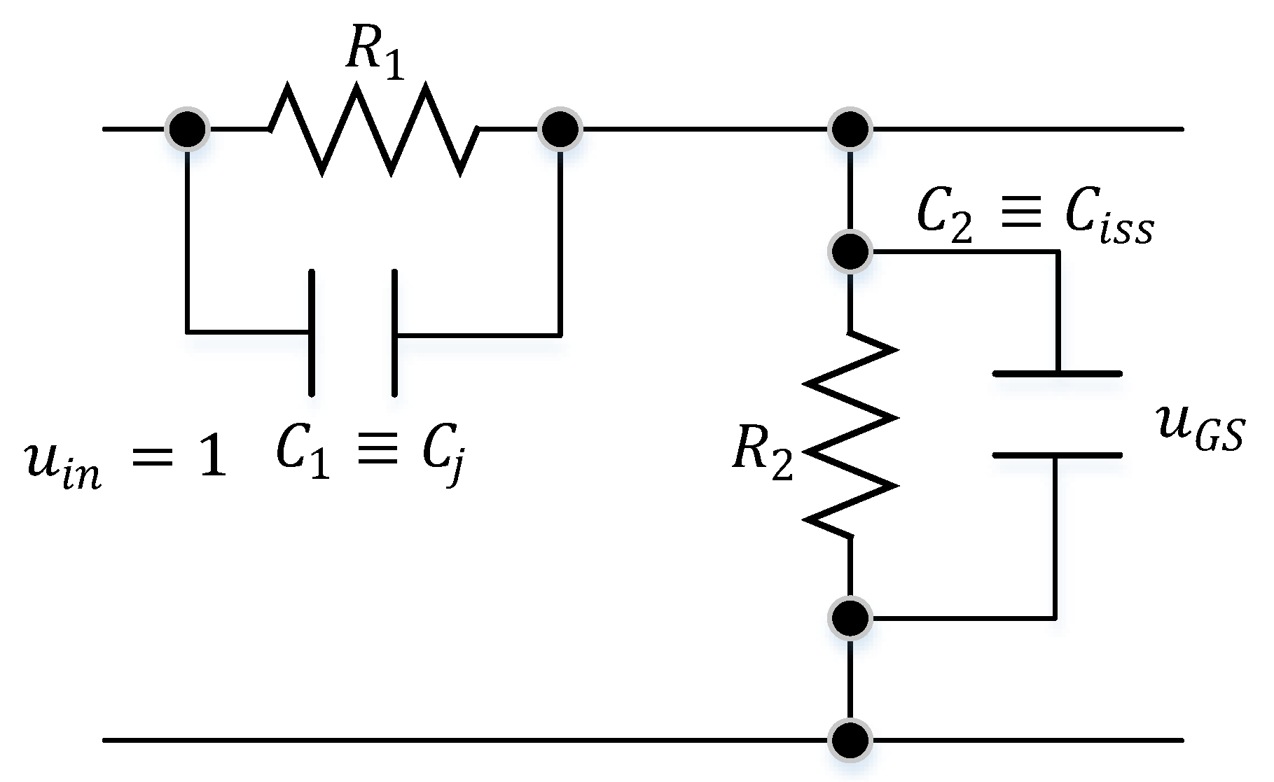
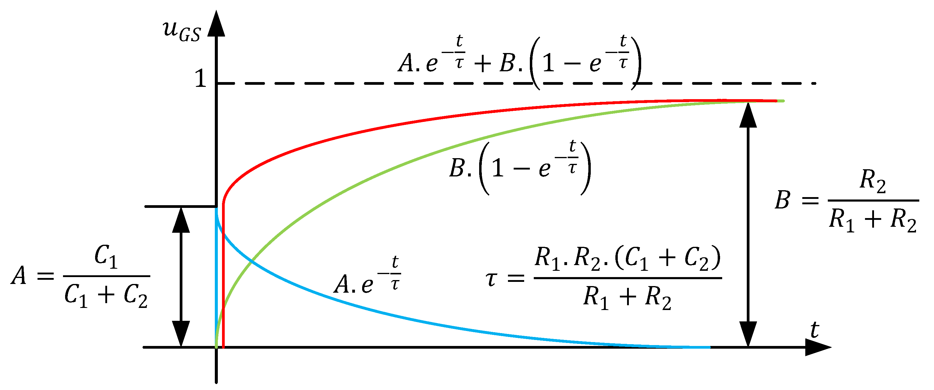
2. Mathematical Descriptions and Study
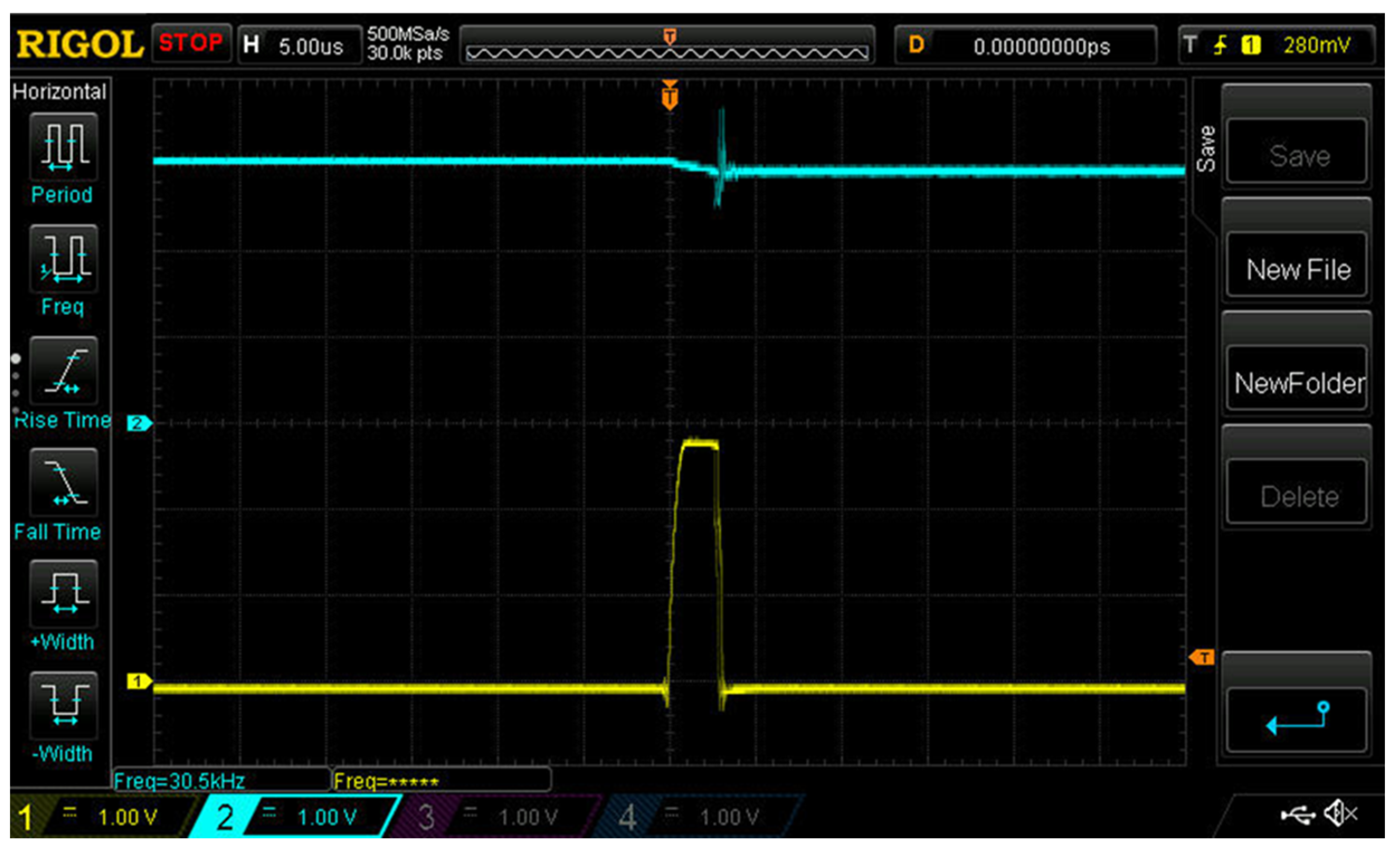
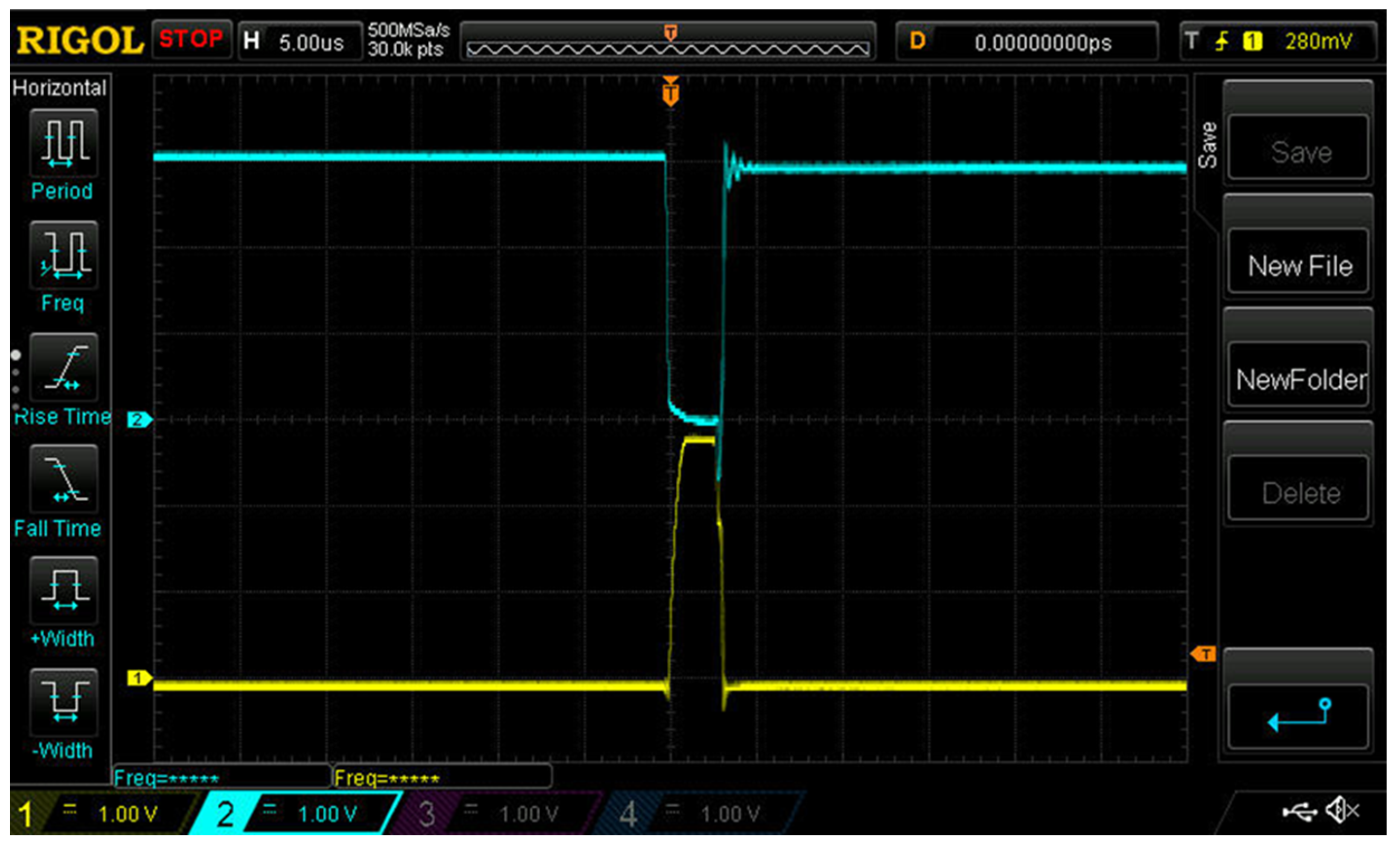
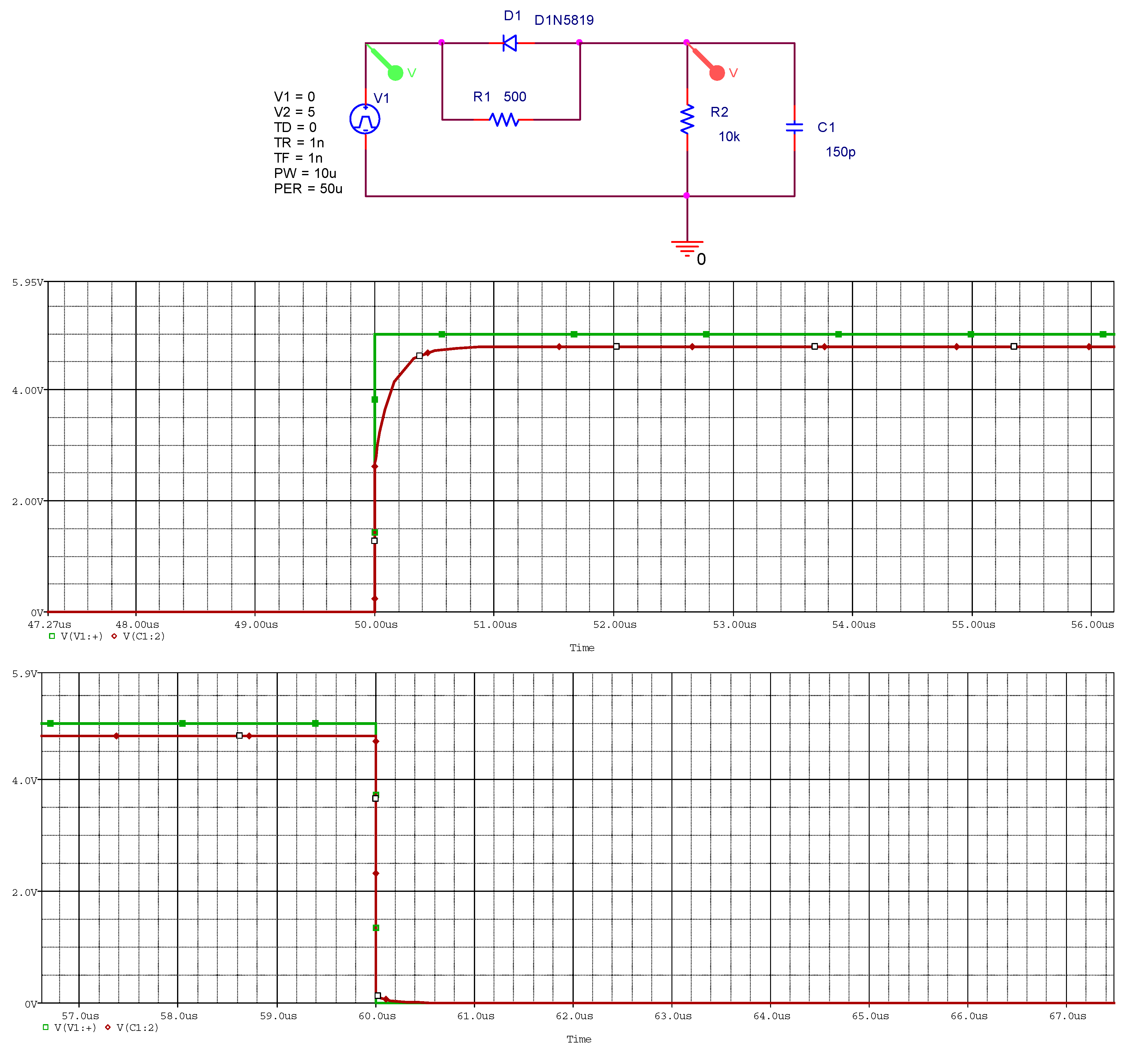
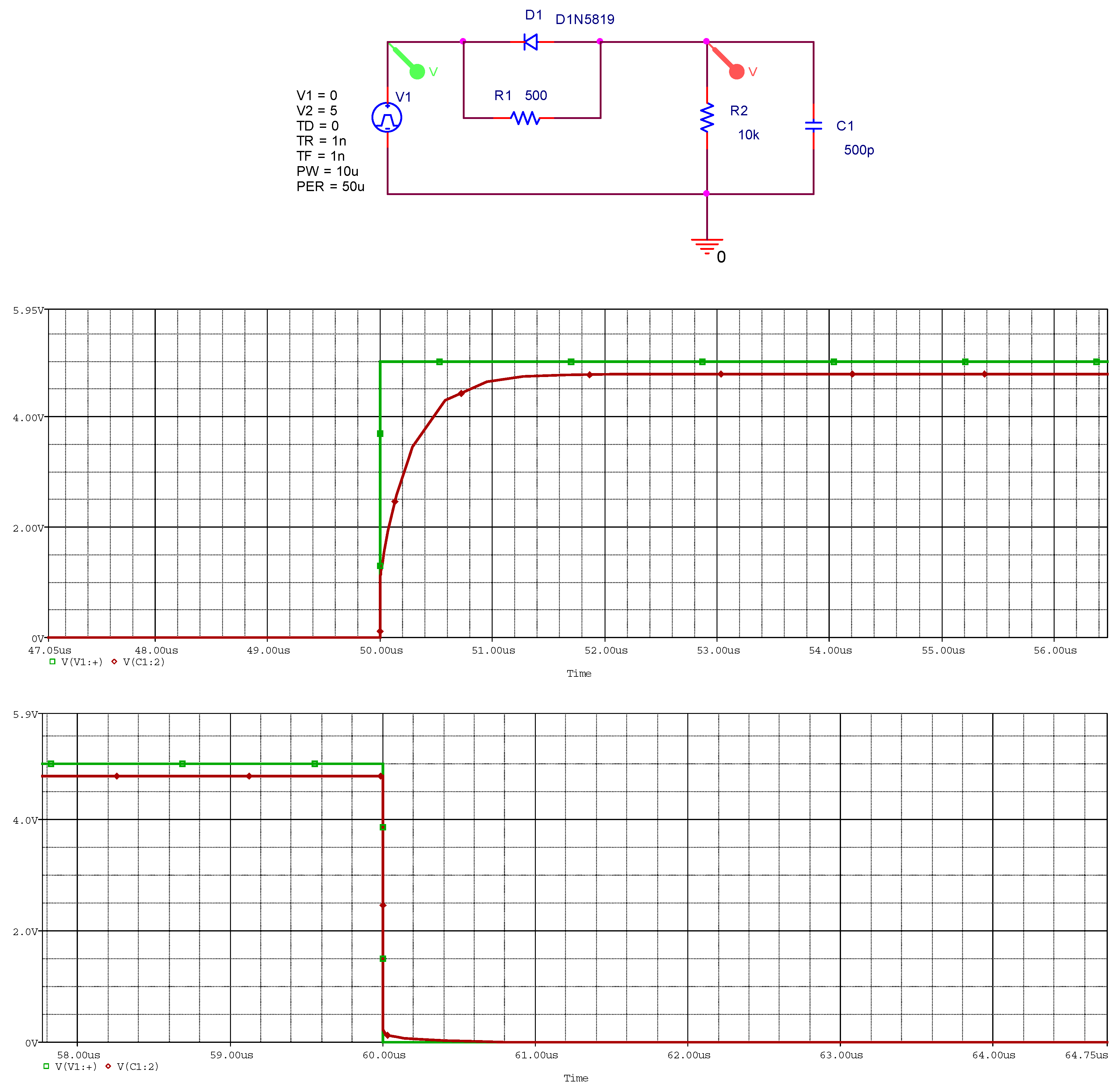
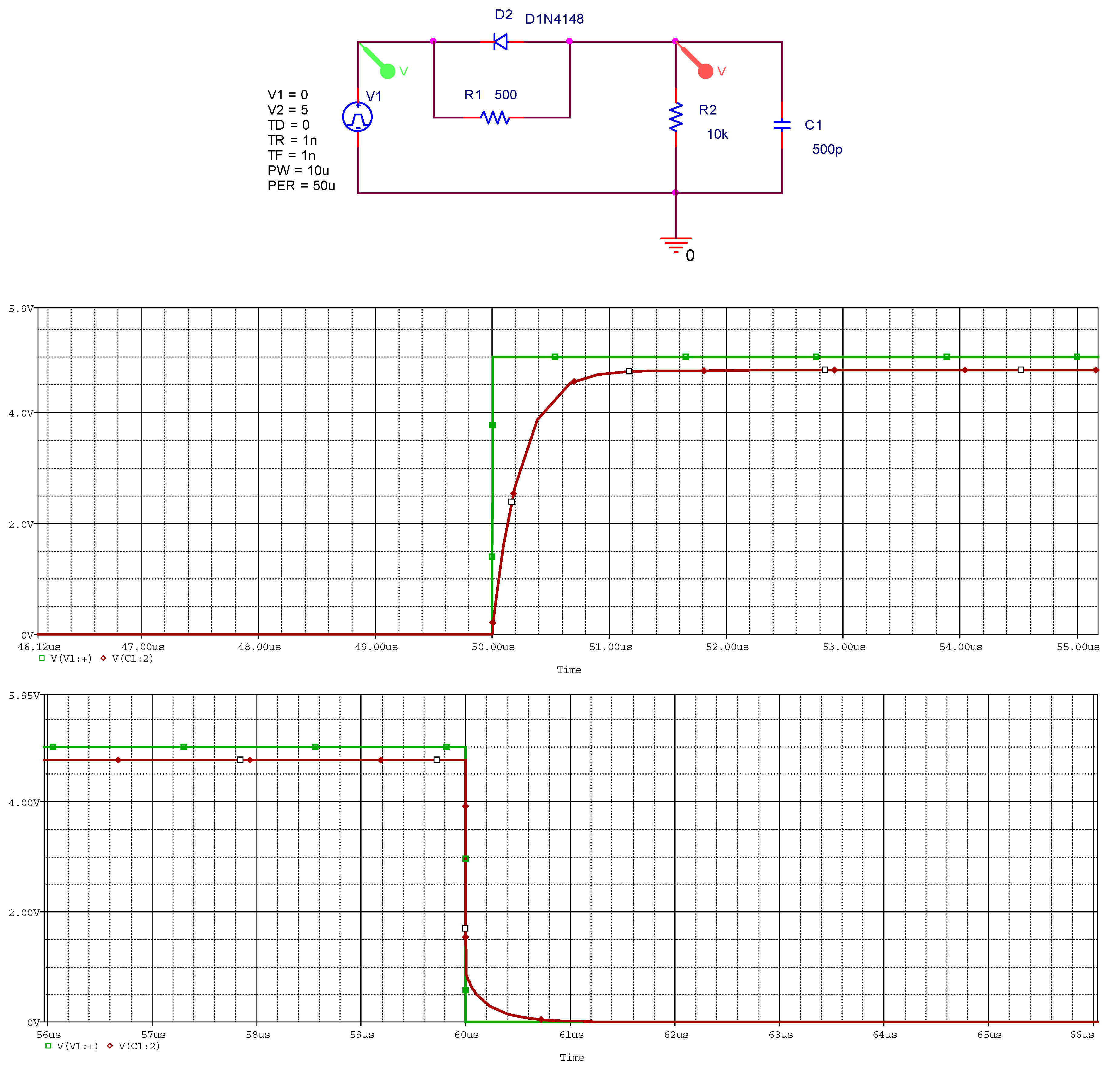
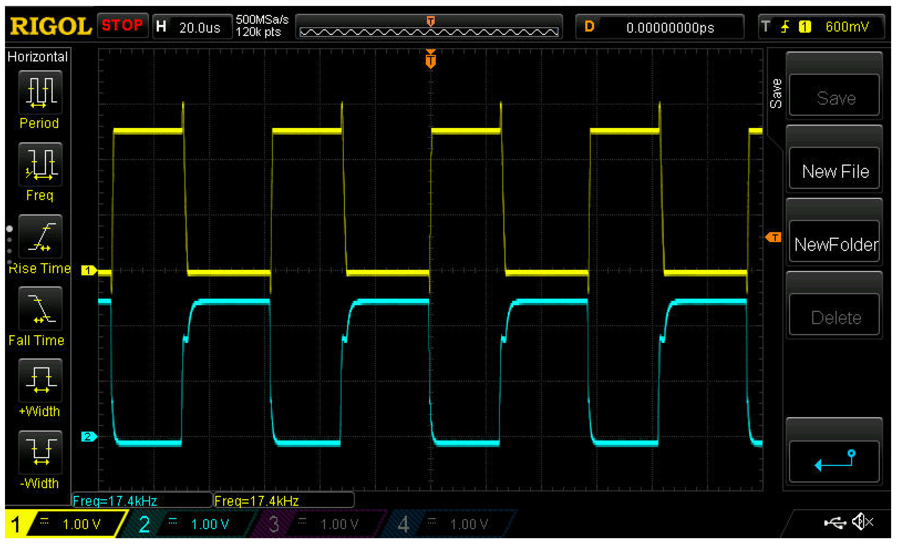
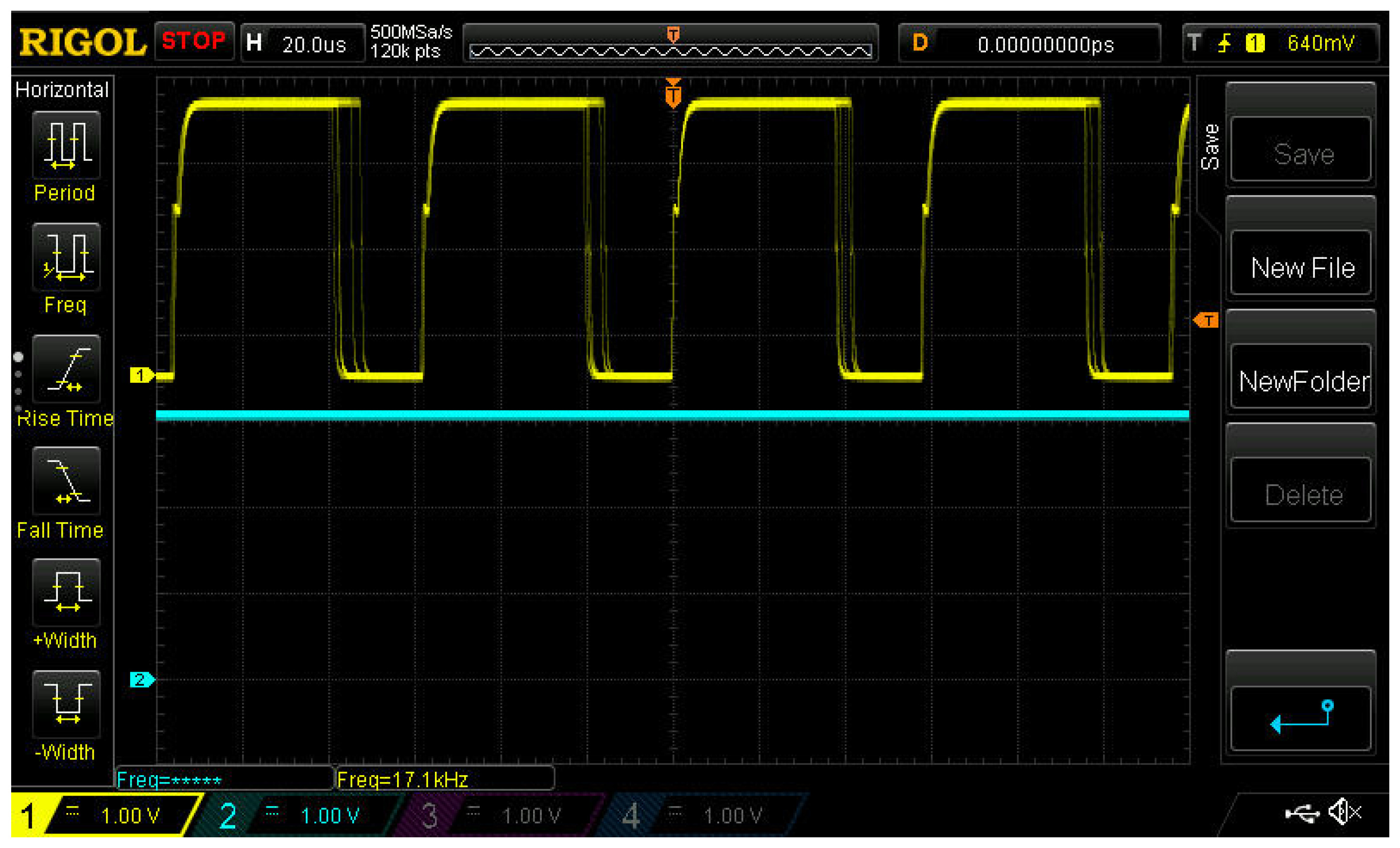
Essential to the solution of the described problem is the consideration of the influence of the Schottky diode capacitance when applying a signal to turn on the transistor. The study was carried out using the circuit shown in Figure 4, where the Schottky diode capacitance C j and the input capacitance of the transistor C i s s were added to the elements D 1 ,   R 1 ,   R 2 in Figure 1. The equivalent circuit for mathematical description is presented in Figure 5.
It was assumed that the input voltage was increased stepwise to a value of 1 (single input pulse u i n = 1 ), and the change in the output voltage u G S , which is the gate-source voltage of the transistor, was examined.
The expressions for the impedances from the circuit in Figure 5 in operator form are as follows:
Z 1 s = R 1 1 + s · R 1 · C 1 ; Z 2 s = R 2 1 + s · R 2 · C 2 .
For a single input, the output voltage has the following form:
u G S s = 1 s . Z 2 s Z 1 s + Z 2 s .
It can also be represented as follows:
u G S s = A a + s + B s a + s ,
where
A = C 1 C 1 + C 2 ,
B = R 2 R 1 + R 2 ,
a = 1 τ ,
τ = R 1 · R 2 · C 1 + C 2 R 1 + R 2 .
When switching from the Laplace domain to the time domain, the change in output voltage over time is obtained:
u G S t = A · e t τ + B · 1 e t τ .
Figure 6 presents the two terms of expression (5)—the first with a blue line, the second—with a green line, and their sum—with a red line.
From Figure 6, it can be observed that the output voltage u G S , which is the gate-source voltage of the transistor, has a sharp increase at the initial moment, which depends on the ratio of the two capacitances C 1 (the capacitance of the Schottky diode) and C 2 (the input capacitance of the MOSFET). For example, if C 2 C 1 the value of the initial increase will be of a negligible value. If the two capacitances are equal, this value will be half the value of the input voltage. However, if C 1 C 2 , the initial increase may be close to the value of the input voltage. This effect is observed in the upper oscillogram of Figure 3. The problem is that, depending on the ratio of the two capacitances, the value of the initial increase may be greater than the value of the threshold voltage U t h of the transistor. In such a situation, “dead time” is not implemented, and the effect described in the introduction is observed.
Formula (5) can be used to determine the value of the “dead time” depending on the value of the resistor R 1 at known other values. For this purpose, it is presented as follows:
u G S t = A B e t τ + B .
By substituting t = t d and u G S t d = U t h , we obtain the following expression:
t d = τ · l n A B U t h B .
Substituting the values from (4) into (7) gives the following:
t d = R 1 · R 2 · C 1 + C 2 R 1 + R 2 · l n C 1 C 1 + C 2 R 2 R 1 + R 2 U t h R 2 R 1 + R 2 .
Since the equations were derived using a unit input, the value of U t h should be set in units relative to the maximum value of the driver’s output voltage. For example, if it is 3 V, and the threshold voltage is 1.8 V, then in Formula (8), U t h = 0.6.
In Formula (8), the capacitance values are known from reference data for the selected elements—Schottky diode, MOSFET, and Zener diode parallel to the gate-source junction. The value of the resistor R 2 is usually 10 K. It remains to calculate the value of t d for different values of R 1 and choose the appropriate value of the resistor.
For example, for variant 4 of Table 1 considered below, the values are as follows: C 1 = 140   p F ; C 2 = 365   p F ; R 2 = 10   K . With a minimum threshold voltage of 1 V for the MOSFET and an output voltage from the driver of 3 V, in Formula (8), U t h = 1 3 0.33 . After calculation, a value of t d = 111 ns is obtained for resistor value R 1 = 500   Ω .
A computer simulation using the program OrCAD 9.2 was performed using models of real diodes and transistors. The results are shown and commented on below.
Variant 1—Schottky diode 1N5819 with a capacitance of 150 pF [26], transistor with an input capacitance of 150 pF. The input signal had a maximum value of 5 V. The simulation circuit and the results are shown in Figure 7.
It can be observed that when a signal was applied to turn on, the initial peak of the output voltage was 2.5 V, consistent with coefficient A in Figure 6. When switched off, an initial retention of about 0.3 V (the voltage across the switched-on Schottky diode) was observed. It is clear that this combination will not achieve “dead time” implementation for transistors with a threshold voltage below 2.5 V.
Variant 2—Schottky diode 1N5819 with a capacitance of 150 pF [26], transistor with an input capacitance of 500 pF. The input signal had a maximum value of 5 V. The simulation circuit and the results are shown in Figure 8.
It can be observed that when a signal was applied to turn on, the initial peak of the output voltage was approximately 1 V, consistent with coefficient A in Figure 6. When switched off, an initial retention of about 0.3 V (the voltage across the switched-on Schottky diode) was observed. It is clear that this combination will not achieve “dead time” implementation for transistors with a threshold voltage below 1 V. When the input capacitance of the transistor increased, the initial spike of the gate-source voltage decreased.
Variant 3—Silicon diode 1N4148 with a capacitance of 3 pF [27], transistor with an input capacitance of 500 pF. The input signal had a maximum value of 5 V. The simulation circuit and the results are presented in Figure 9. This variant was chosen because pulse diodes with a PN junction are characterized by significantly lower capacitance values.
This variant corresponds to the condition C 2 C 1 .
It can be observed that when a signal was applied to turn on, the initial peak of the output voltage was negligibly small, consistent with coefficient A in Figure 6. It is clear that this combination makes implementing “dead time” when turning on the lower transistor easiest even at low threshold voltages. When turning off, an initial voltage retention of about 0.7 V (the voltage across the switched-on diode) was observed. However, this is problematic since, at the same moment, a signal is applied to turn on the upper transistor of the synchronous converter, and if the lower transistor has a threshold voltage of approximately 0.7 V, it may remain on for a short time. This would make it difficult to implement “dead time” when turning on the upper transistor. For this reason, the authors recommend using Schottky diodes, as shown in the circuit in Figure 1.
Variant 4Connecting a Zener diode in parallel with the gate-source junction of the transistor. The diode has protective functions described in the literature [8,9]. The schematic diagram together with the capacitances is shown in Figure 10: Schottky diode 1N5819 with a capacitance of 150 pF [23], transistor with an input capacitance of 500 pF, Zener diode BZX84C5V6 surface-mount device with a capacitance of 200 pF [28]. The input signal had a maximum value of 5 V. The simulation circuit and the results are shown in Figure 11.
This variant differs from variant 2 only in the inclusion of the Zener diode. Comparison of the timing diagrams in Figure 11 with those in Figure 8 shows that the initial peak was reduced to about 0.9 V, which would facilitate the implementation of “dead time” for transistors with a threshold voltage above 1 V. In addition to the protective function, the authors recommend placing a Zener diode for the reasons discussed in this article as well.

3. Experiment

The initially implemented variant for the lower transistor in Figure 1 is the following: transistor BSS214N with capacitance C i s s = 107   p F and threshold voltage U t h = 0.7   V [29] and a Schottky diode SS34 with capacitance C j = 1   n F ÷ 500   p F [30]. The oscillograms shown in Figure 2 and Figure 3 correspond to this variant. From the previous consideration, it is clear that this variant is unsuitable. Table 1 shows various possible variants for implementation—combinations of Schottky diodes and transistors with or without a Zener diode. Those shown in red are unsuitable, while the one in yellow is not preferable, since the results are close to the limit. From the point of view of “dead time”, variants 4, 5, and 6 are suitable—as shown in green. Variants 5 and 6 are not preferred due to the considerations expressed when commenting on the results in Figure 9. The preferred implementation variant is 4, shown in blue in the first column of Table 1. It uses a Schottky diode SS14, which has a significantly lower capacitance than SS34 [31].
The last three variants in Table 1 were evaluated from the following point of view: when turning on the upper transistor in Figure 1 and increasing the voltage at point A, through the feedback capacitance C r s s of the lower transistor, its gate-source capacitance is charged (Miller effect) [32]. Shortly before this (to ensure the “dead time”), there is a low level at the driver output. In this situation, due to the feedback, the input capacitance would be charged to a voltage equal to the sum of the voltage drop on the Schottky diode (or the pulse diode with a PN junction) and the voltage on the lower transistor of the driver. This sum of voltages must remain less than the threshold voltage of the lower transistor, otherwise it may turn on as well. With a sharp increase in voltage at point A, the consideration made in the previous part can be applied. The results in Table 2 show that from such a point of view, variants 5 and 6 are borderline (shown in yellow). Variant 4 (in green) is also suitable in this regard.
After the implementation assessment, variant 4 was chosen, and the section of the board corresponding to the circuit under consideration is shown in Figure 12. All electronic components correspond to variant 4 (shown in blue in the first column of Table 2).
In the variants presented in the two tables, the authors compared the possibilities for an accessible and quick solution to the problem described at the beginning of the article. Other combinations of MOSFETs, Schottky diodes, and Zener diodes are also possible. During initial development, different options should be sought and evaluated in terms of price and market availability before a choice is made.
Schottky diodes D 6 and D 7 were SS14 and correspond to D 2 and D 1 in Figure 1. Resistors R 10 and R 13 consisted of two parallel-connected resistors with a value of 1 K and correspond to R 3 and R 1 in Figure 1. Resistors R 9 and R 10 had a value of 10 K and correspond to R 4 and R 2 in Figure 1. Zener diodes BZM55C5V1 were soldered to these resistors. Transistor M1 (P-channel) was BSP250. Transistor M2 (N-channel) was UT6402G. The two drains pins were connected externally to the left terminal of the inductor in the circuit if Figure 1 (point A—Figure 1).
Figure 13 and Figure 14 show the recorded oscillograms. The operating frequency of the converter was 17 kHz, and the supply voltage was 3.3 V.
From CH2 in Figure 13, the gradual increase in the gate-source voltage of the N-channel transistor when turned on (to implement “dead time” when turning off the P-channel transistor) and a rapid decrease (to implement “dead time” when turning on the P-channel transistor) are observed.
From CH2 in Figure 14, it can be observed that there were no short-term dips in the supply voltage both during switching on and off of the N-channel transistor. The measured current consumed by the power source in this case was significantly lower than in the case shown in Figure 2. This is proofs of the correct implementation of “dead time” according to the circuit in Figure 10 for the two transistors in a synchronous step-down converter.
It should be noted that with a change in temperature, the parameters of the diodes and the transistor change. The authors worked with the minimum threshold voltage of transistor UT6402 at the highest temperature, taken from the graphical dependence in [33].

4. Conclusions

The paper investigated the “dead time” of a synchronous step-down converter implemented with P-channel and N-channel transistors. The implementation of “dead time” with external components when controlled by a driver with a push–pull output was considered. The main attention was paid to the influence of the Schottky diode capacitance. The main conclusions are as follows:
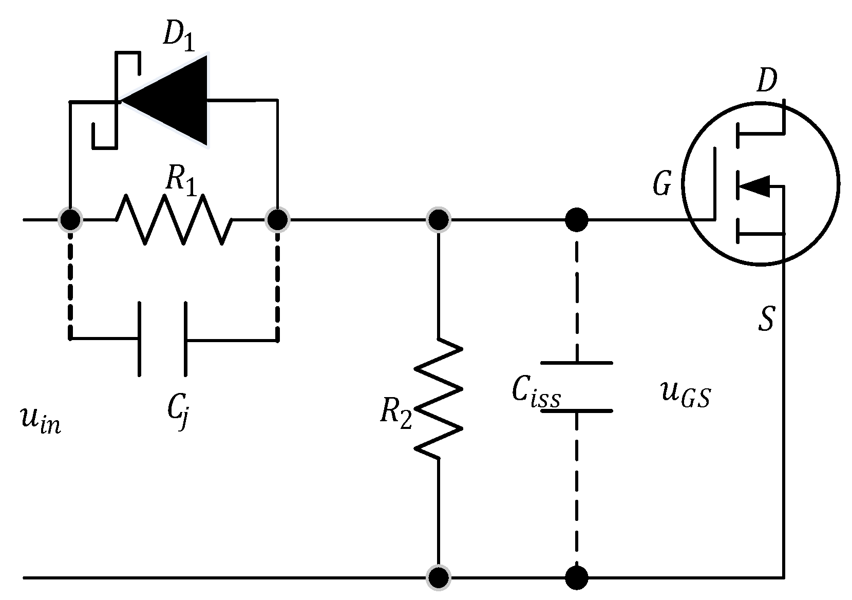
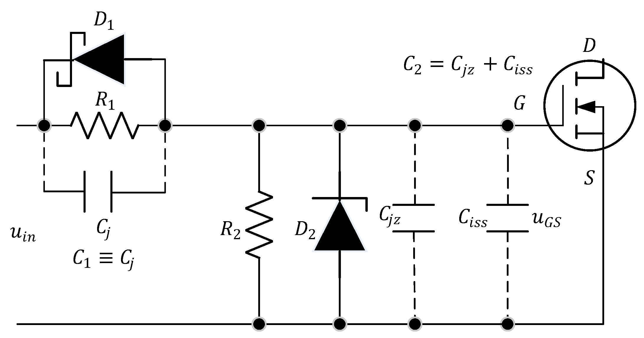
  • It is recommended to implement external circuits for the gate of the transistor according to the circuit in Figure 10.
  • When designing “dead time” circuits, it is necessary that the Schottky diode capacitance be significantly lower than the input capacitance of the transistor.
  • Based on Formula (5) and Figure 6, compliance with the threshold voltage of the MOSFET must also be checked.
  • It is not recommended to use a pulse diode with a PN junction instead of a Schottky diode due to the larger forward voltage drop across the diode with a PN junction. When the upper transistor is turned on, due to feedback capacitance, it is possible for the input capacitance of the lower transistor to be charged to a voltage higher than the threshold voltage.
  • It is recommended to include Zener diodes with the lowest possible reference voltage (but greater than the maximum threshold voltage of the lower transistor) in parallel with the gate-source junction. Zener diodes with a lower reference voltage have a greater capacitance. In addition to their protective function, these diodes also facilitate the implementation of “dead time.”
  • Formula (8) can be used to determine the value of “dead time” t d at different values of the resistor R 1 and known values of the other quantities.
The considerations and conclusions presented in this article refer not only to the circuit in Figure 1. They can be applied in all cases of implementation of “dead time” according to the circuit of Figure 10.
The results obtained in this article can be applied to low-power systems such as energy harvesting systems, for example, with a piezoelectric element or a small photovoltaic system; battery or ultracapacitor charging systems; and powering IoT systems.

Author Contributions

Conceptualization, H.A.; Methodology, H.A.; Software, D.B.; Validation, H.A.; Investigation, H.A.; Writing – original draft, H.A. and D.B.; Visualization, D.B.; Supervision, H.A. All authors have read and agreed to the published version of the manuscript.

Funding

This study was funded by the European Union—Next Generation EU through the National Recovery and Resilience Plan of the Republic of Bulgaria, project No. BG-RRP-2.004-0002, “BiOgraMCT.”

Data Availability Statement

Data are contained within the article.

Acknowledgments

The authors express their gratitude to the Rector and management of the University of Chemical Technology and Metallurgy, Sofia, Bulgaria, for the financial support in publishing this article.

Conflicts of Interest

The authors declare no conflicts of interest.

Abbreviations

The following abbreviations were used in this manuscript:
CHchannel
DCdirect current
MOSFETmetal-oxide-semiconductor field-effect transistor
SMDsurface-mount device
Symbols
C capacitor
D diode
C i s s input capacitance of a MOSFET
C j capacitance of Schottky diode
C j z capacitance of Zener diode
C r s s feedback capacitance of a MOSFET
R resistor
t time
t d duration of “dead time”
U voltage
u G S gate-source voltage of a MOSFET
u i n input voltage
U t h threshold voltage of a MOSFET
τ time constant

References

  1. Jaunay, S.; Broun, J. DC-to-DC Design Guide, Vishay Siliconix, Application Note AN607, Document Number 71917, 10 October 2002. Available online: https://www.vishay.com/docs/71917/71917.pdf (accessed on 1 December 2023).
  2. Hudson, T. The Difference Between CCM and DCM Explained; Article #A-0022 Rev. 1.0; Monolithic Power System: Washington, DC, USA, 2022. [Google Scholar]
  3. Maxim Integrated. Synchronous Rectification Aids Low-Voltage Power Supplies, Application Note 652, 31 Janunary 2001. Available online: http://www.maximintegrated.com/an652 (accessed on 1 December 2023).
  4. Rohm Co. Efficiency of Buck Converter, Application Note No. 64AN035E Rev.004. November 2022. Available online: https://fscdn.rohm.com/en/products/databook/applinote/ic/power/switching_regulator/buck_converter_efficiency_app-e.pdf (accessed on 1 August 2024).
  5. Raj, A. Calculating Efficiency, Texas Instruments Application Report SLVA390A-February 2010- Revised March 2020. Available online: https://www.ti.com/lit/an/slva390a/slva390a.pdf?ts=1740203931564&ref_url=https%253A%252F%252Fwww.google.com.hk%252F (accessed on 1 August 2024).
  6. He, X.; Li, D.; Zhang, V. An Accurate Approach for Calculating Efficiency of a Synchronous Buck Converter Using the MOSFET Plateau Voltage, Texas Instruments Application Report SLVAEQ9-July 2020. Available online: https://www.ti.com/lit/an/slvaeq9/slvaeq9.pdf?ts=1740124287780&ref_url=https%253A%252F%252Fwww.google.com%252F (accessed on 1 August 2024).
  7. Klein, J. “Shoot-through” in Synchronous Buck Converter, Fairchild, Application Note AN-6003, 25 April 2003. Available online: www.fairchildsemi.com (accessed on 1 December 2023).
  8. Rohm Co. Basics and Design Guidelines for Gate Drive Circuits, Application Note, No.66AN032E Rev.003, November 2023. Available online: https://fscdn.rohm.com/en/products/databook/applinote/discrete/sic/mosfet/gate_drive_circuit-design_guidelines_an-e.pdf (accessed on 1 May 2024).
  9. Toshiba. MOSFET Gate Drive Circuit, Application Note, 26 July 2018. Available online: https://toshiba.semicon-storage.com/info/application_note_en_20180726_AKX00068.pdf?did=59460 (accessed on 1 December 2023).
  10. Green, P.B.; Zheng, L.; Gate Drive for Power MOSFET in Switching Applications. A Guide for Device Characteristics and Gate Drive Techniques, Infineon Application Note, AN 2203 PL18 2204 004502, V1.0 20 April 2022. Available online: https://www.infineon.com/dgdl/Infineon (accessed on 1 December 2023).
  11. Texas Instruments. Fundamentals of MOSFET and IGBT Gate Drive Circuits, Application Report, SLUA618A-March2017-Revised October 2018. Available online: https://www.ti.com/lit/ml/slua618a/slua618a.pdf?ts=1740191454837&ref_url=https%253A%252F%252Fwww.perplexity.ai%252F (accessed on 1 December 2023).
  12. On Semiconductor. Drive and Layout Requirements for Fast Switching High Voltage MOSFETs. Available online: https://www.onsemi.co/pub/collateral/tnd6242.pdf (accessed on 1 October 2024).
  13. Fairchild, Design and Application Guide of Bootstrap Circuit for High-Voltage Gate-Drive IC, Application Note, AN-6076, 2008, Rev. 1.4*12/18/14. Available online: https://www.onsemi.jppub/collateral/an-6076jp.pdf (accessed on 1 December 2023).
  14. Ji, Y.; Yang, Y.; Zhou, J.; Ding, H.; Guo, X.; Padmanaban, S. Control strategies of mitigating dead-time effect on power converters: An overview. Electronics 2019, 8, 196. [Google Scholar] [CrossRef]
  15. Zhen, S.; Zhang, B.; Luo, P.; Yang, K.; Zhu, X.; Li, J. A high efficiency synchronous buck converter with adaptive dead time control for dynamic voltage scaling applications. In Proceedings of the 2011 IEEE/IFIP 19th International Conference on VLSI and System-on-Chip, Hong Kong, China, 3–5 October 2011; pp. 43–48. [Google Scholar] [CrossRef]
  16. Lee, S.; Jung, S.; Park, C.; Rim, C.T.; Cho, G.H. Accurate Dead-Time Control for Synchronous Buck Converter With Fast Error Sensing Circuits. IEEE Trans. Circuits Syst. I Regul. Pap. 2013, 60, 3080–3089. [Google Scholar] [CrossRef]
  17. Floriberto, A.L.; Santos, M.B.; Barata, J.; Aguiar, J. Dead-Time Control System for a Synchronous Buck dc-dc Converter. In Proceedings of the 2007 International Conference on Power Engineering, Energy and Electrical Drives, Setubal, Portugal, 12–14 April 2007; pp. 423–428. [Google Scholar]
  18. Zhou, M.; Low, Q.; Siek, L. A high efficiency synchronous buck converter with adaptive dead-time control. In Proceedings of the 2016 International Symposium on Integrated Circuits (ISIC), Singapore, 12–14 December 2016; pp. 1–4. [Google Scholar] [CrossRef]
  19. Yan, W.; Pi, C.; Li, W.; Liu, R. Dynamic dead-time controller for synchronous buck DC-DC converters. Electron. Lett. 2010, 46, 164–165. [Google Scholar] [CrossRef]
  20. Himabindu, M.; Gupta, M.; Singh, S.; Chandra, P.K.; Alkhafaji, M.A. Adaptive Dead-Time Compensation in Synchronous Buck Converters for Enhanced Efficiency in IoT Applications. In Proceedings of the 2023 International Conference on Power Energy, Environment & Intelligent Control (PEEIC), Greater Noida, India, 19–23 December 2023; pp. 408–412. [Google Scholar] [CrossRef]
  21. Thuc, G.H.; Chen, C.-J. An Integrated Driver With Dual-Edge Adaptive Dead-Time Control for GaN-Based Synchronous Buck Converter. IEEE Trans. Ind. Appl. 2024, 60, 9157–9170. [Google Scholar] [CrossRef]
  22. Lee, Y.; Kim, D.; Kim, J. A GaN Driver IC With a TDC-Based Dead-Time Controller For GaN DC-DC Buck Converters. In Proceedings of the 2023 20th International SoC Design Conference (ISOCC), Jeju, Republic of Korea, 25–28 October 2023; pp. 33–34. [Google Scholar] [CrossRef]
  23. Texas Instruments. TPS2836, TPS2837 Synchronous-Buck MOSFET Driver with Dead-Time Control, Application Note SLVS 224B-November 1999-Revised August 2002. Available online: https://www.ti.com/lit/ds/symlink/tps2837.pdf?ts=1740147699986 (accessed on 1 February 2025).
  24. Zhang, Y.; Wang, J. Understanding Dead-Time Based on TPS51225/275/285, Texas Instruments Application Report SLUA919-August 2018. Available online: https://www.ti.com/lit/an/slua919/slua919.pdf?ts=1740147700257 (accessed on 1 February 2025).
  25. Nexperia. Trench Schottky Diodes in Modern Swithing Applications, Application Note AN90056, Rev.1.0-9 September 2024. Available online: https://assets.nexperia.com/documents/application-note/AN90056.pdf?__hstc=13651368.2f3f33a24b44870ec4a577029c49e44b.1725840002137.1725840002138.1725840002139.1&__hssc=13651368.1.1725840002140&__hsfp=2420521548 (accessed on 1 February 2025).
  26. Vishay. 1N5817, 1N5818, 1N5819 Schottky Barier Plastic Rectifier, Data Sheet, Document Number 88525, Revision 1 July 2020. Available online: https://www.vishay.com/docs/88525/1n5817.pdf (accessed on 1 October 2024).
  27. Vishay. 1N4148WS Small Signal Switching Diode, Data Sheet, Document Number 85751, Revision 6 July 2017. Available online: https://www.vishay.com/zh/product/85751/ (accessed on 1 October 2024).
  28. On Semiconductors. BZX84C3V3- BZX84C33 Zeners, Data Sheet, November 2015. Available online: https://media.digikey.com/pdf/Data%20Sheets/ON%20Semiconductor%20PDFs/BZX84C3V3-C33_Rev1.10_Nov2015.pdf (accessed on 1 October 2024).
  29. Infineon. BSS214N OptiMOS 2 Small-Signal Transistor, Data Sheet, Rev.2, 08-07-2011. Available online: https://www.infineon.com/dgdl/Infineon-BSS214N-DS-v02_03-en.pdf?fileId=db3a304330f6860601311828a70444e9 (accessed on 1 October 2024).
  30. Vishay. SS32, SS33, SS34, SS35, SS36 Surface-Mount Schottky Barier Rectifier, Data Sheet, Document Number 88751, 23-April-2020. Available online: https://www.vishay.com/docs/88751/ss32.pdf (accessed on 1 October 2024).
  31. Vishay. SS12, SS13, SS14, SS15, SS16 SS36 Surface-Mount Schottky Barier Rectifier, Data Sheet, Document Number 88746, 23-April-2020. Available online: https://www.vishay.com/docs/88746/ss12.pdf (accessed on 1 October 2024).
  32. Bakhordarian, V. Power MOSFET Basics, International Rectifier, an-1084, p1–p65. Available online: https://www.tayloredge.com/reference/Electronics/Semiconductors/mosfetbasics.pdf (accessed on 1 October 2024).
  33. Unisonic Technologies. UT6402 Power MOSFET N-Channel Enhancement Mode, Document No QW-502-152E, 2023. Available online: https://www.unisonic.com.tw/uploadfiles/836/part_no_pdf/UT6402.pdf (accessed on 1 October 2024).
Figure 1. Implementation with P-channel and N-channel MOSFETs and control with a driver with a push–pull output.
Energies 18 01095 g001
Figure 2. CH1—supply voltage of 3.3 V, CH2—voltage at point A.
Energies 18 01095 g002
Figure 3. CH1—impulse of the lower transistor, CH2—voltage at point A.
Energies 18 01095 g003
Figure 4. Circuit for studying the influence of the Schottky diode capacitance when applying a signal to turn on the transistor.
Energies 18 01095 g004
Figure 5. Mathematical description circuit: C 1 C j ;   C 2 C i s s .
Energies 18 01095 g005
Figure 6. Variation of the output voltage over time—the red line.
Energies 18 01095 g006
Figure 7. Simulation circuit and the results for variant 1.
Energies 18 01095 g007
Figure 8. Simulation circuit and the results for variant 2.
Energies 18 01095 g008
Figure 9. Simulation circuit and the results for variant 3.
Energies 18 01095 g009
Figure 10. Connecting a Zener diode in parallel with the gate-source junction of the transistor.
Energies 18 01095 g010
Figure 11. Simulation circuit and the results for variant 4.
Energies 18 01095 g011
Figure 12. A picture of the power schematic section.
Energies 18 01095 g012
Figure 13. CH1—voltage at point A; CH2—pulses to control the lower transistor.
Energies 18 01095 g013
Figure 14. CH1—control pulses of the lower transistor, CH2—supply voltage.
Energies 18 01095 g014
Table 1. Variants for providing “dead time” for a signal to turn on the lower transistor.
Schottky Diode
(Diode) Capacitance, pF
Transistor, Zener Diode
Capacitance, pF
Value of A,
Starting Voltage G-S at 3 V from the Driver, V
Transistor   U G S t h , min. Value, V
Variant 1SS34,   C j = 500   p F BSS214N, C i s s = 107   p F 0.837, 2.51 V0.7
Variant 2SS34, C j = 500   p F UT6402G, C i s s = 265   p F 0.654, 1.962 V1.0
Variant 3SS14, C j = 140   p F UT6402G, C i s s = 265   p F 0.345, 1.035 V1.0
Variant 4SS14, C j = 140   p F UT6402G, C i s s = 265   p F ,
BZM55C5V1, C j z = 100   p F
0.277, 0.831 V1.0
Variant 51N4148W-G, C j = 2   p F UT6402G, C i s s = 265   p F 0.0075, 0.0225 V1.0
Variant 61N4148W-G, C j = 2 p F UT6402G, C i s s = 265 p F ,
BZM55C5V1, C j z = 100   p F
0.00544, 0.0163 V1.0
Table 2. Ensuring the off state of the lower transistor through the feedback capacitance when the upper transistor is turned on.
Schottky Diode (Diode),
Forward Voltage, V
Driver Output Low Voltage, V
UT 6402 G ,   C R s s = 56   p F Value of Starting Voltage
G-S at 3 V from D-S,V
Transistor   U G S t h , min. Value, V
Variant 4SS14, 0.3   V ,
LPV7215, V o L = 0.3   V
Total, 0.6 V < 1 V
UT6402G, C i s s = 265   p F ,
BZM55C5V1, C j z = 100   p F
0.4 V1.0
Variant 51N4148W-G, 0.75   V
LPV7215, V o L = 0.3   V
Total, 1.05 V > 1 V
UT6402G, C i s s = 265   p F 0.523 V1.0
Variant 61N4148W-G, 0.75   V
LPV7215, V o L = 0.3   V
Total, 1.05 V > 1 V
UT6402G, C i s s = 265   p F ,
BZM55C5V1, C j z = 100   p F
0.4 V1.0
Disclaimer/Publisher’s Note: The statements, opinions and data contained in all publications are solely those of the individual author(s) and contributor(s) and not of MDPI and/or the editor(s). MDPI and/or the editor(s) disclaim responsibility for any injury to people or property resulting from any ideas, methods, instructions or products referred to in the content.

