1. Introduction
The Internet of Things (IoT) has become an integral part of the modern world, transforming how people interact with technology and positively influencing numerous sectors globally. IoT devices are characterized by their ability to communicate and exchange data over the internet without human intervention. This capability has driven their exponential adoption across diverse industries. From smart homes and smart cities to transportation, agriculture, pollution monitoring, and healthcare, IoT applications have touched nearly every aspect of life [
1]. These devices have significantly improved efficiency, productivity, and convenience in various domains. However, the effectiveness of IoT applications depends on the long-term operation of these devices, which, in turn, requires efficient power sources.
The power requirements of IoT devices vary depending on the application. While some devices demand minimal energy, others require substantial power to function effectively. This diversity in energy needs poses challenges, particularly for battery-powered devices with limited lifespans. Consequently, developing innovative energy solutions is essential to overcome these challenges.
Energy harvesting techniques have emerged as a promising solution to power IoT devices efficiently. These techniques involve capturing and converting energy from environmental sources into electrical power. For instance, kinetic energy, thermal energy, and radio frequency (RF) energy can all be harvested. Kinetic energy harvesting converts motion or vibrations into electricity [
2], while thermal energy harvesting utilizes temperature differences to generate power [
3]. RF energy harvesting, on the other hand, collects energy from radio frequency signals emitted by devices in the environment and converts it into DC electricity [
4].
Among the various energy harvesting technologies, RF energy harvesting has gained significant attention for its potential to power IoT devices and other applications requiring wireless power transfer. For example, wireless power transfer (WPT) technology has been successfully implemented in medical applications, such as charging implanted medical devices, eliminating the need for additional surgeries [
5]. Adapting similar RF energy harvesting principles can significantly enhance device performance and usability. Implementing RF energy harvesters provides several advantages, including extended device lifespan, reduced environmental impact by decreasing reliance on traditional batteries, and enabling dynamic energy recharging [
6]. Research has demonstrated the transformative potential of energy harvesting systems, which can extend device lifetimes by reducing battery capacity or even eliminating the need for batteries altogether [
7]. This highlights the growing emphasis on sustainable and autonomous energy solutions across diverse applications, particularly for IoT devices. However, optimizing the efficiency and reliability of RF energy harvesters remains a key challenge to their widespread adoption in IoT systems.
The study of previous research on rectifier designs provides a solid foundation for understanding the development of energy harvesting technologies and establishes a benchmark for advancements in this work. Many rectifiers have been designed to operate around the 900 MHz frequency. For instance, an eight-stage Dickson charge pump implemented at 925 MHz achieved a peak power conversion efficiency (PCE) of 43.26% at an input power of −21.2 dBm [
8]. Similarly, a three-stage Dickson charge pump designed for 953 MHz using the global foundries process reported a PCE of 84.37% at an input power level of −15 dBm [
8]. These energy harvester systems utilized the Dickson charge pump design due to its numerous advantages, including effective operation at high frequencies and a straightforward structure that simplifies rectifier topologies in various applications.
Advancements in rectifier designs have also played a crucial role in improving the efficiency of energy harvesting systems. The adoption of square waves to drive transmitting power transducers has demonstrated higher power effectiveness, with peak power conversion efficiency and power density reaching 95% and 222 mW/mm
2, respectively [
9]. This showcases the potential of cutting-edge designs to achieve high-efficiency energy conversion, essential for supporting IoT applications.
Some designs have employed alternative rectifier topologies. For example, a single-stage differential cross-coupled rectifier was implemented at 900 MHz, achieving a PCE of 67.5% with an input power of −12.5 dBm and an output voltage of 0.62 V [
10]. While this design minimizes the transistor’s on-resistance, it is limited to low-frequency applications. Another example is a five-stage gate-boosting rectifier designed at 900 MHz, which achieved a PCE of 31.8% with an input power of 18 dBm and an output voltage of 6 V [
11]. However, its complex structure and the need for additional circuitry to implement the gate-boosting technique present significant challenges.
With the 5.8 GHz band widely used in applications like Wi-Fi (802.11a) [
12], ISM (industrial, scientific, and medical) bands and microwave communications, the RF energy emitted from such sources can be harvested as well. This will enable the CMOS energy harvesters to integrate seamlessly with portable or miniaturized systems like wearables and sensors as they have small form factor and integrated antennas.
Several on-chip rectifiers have been developed for operation around 5.8 GHz, employing diverse configurations to optimize performance for specific applications. A notable design is a single-series rectifier circuit operating at 5.9 GHz with an input RF power of 0 dBm, achieving a PCE of 52% and a DC output voltage of 1.31 V [
13]. This design is suitable for low-power applications due to its simplicity and low voltage drop. However, it suffers from efficiency limitations at low input voltage levels, reducing its effectiveness for IoT applications. Another example is a single-stage Dickson charge pump rectifier optimized for 5.2 GHz, which achieved a PCE of 64.1%, a DC output voltage of 5.1 V, and an input power of 24 dBm [
14]. While the Dickson charge pump design offers low turn-on voltage and a simple structure, its efficiency is high only at relatively high input power levels, limiting its application in low-power systems.
A two-stage differential drive rectifier (DDR) designed using 65 nm CMOS technology for operation at 5.8 GHz achieved a maximum PCE of 71.8% with an input power of −12.5 dBm and an output voltage of 1.2 V [
15]. Despite its high efficiency at high frequencies, the two-stage configuration introduces additional parasitic effects and power losses due to its increased complexity.
Further studies on rectifiers designed specifically for 5.8 GHz explore various topologies and configurations. For example, a single-diode rectifier operating at 5.8 GHz achieved a PCE of 24% with an input power of −10 dBm [
16], but its low efficiency limits its utility for high-performance energy conversion. Another study focused on a rectifier based on a voltage doubler topology at 5.8 GHz, achieving a PCE of 74.38% with an input power of 10 dBm [
17]. However, the increased layout complexity of this design may impact its reliability and performance in practical applications.
A single-shunt rectifier circuit implemented at 5.8 GHz achieved a PCE of 66% at an input power of 20 dBm using ADS software [
18]. Although the shunt configuration is simple and effective in converting RF power to DC, it requires higher input power levels for optimal efficiency, which limits its applicability in low-power environments. Similarly, a series-shunt rectifier designed for 5.8 GHz operation achieved a PCE of 68.8% with an input power of 10 dBm [
19]. While combining series and shunt configurations improves efficiency, it also introduces layout and manufacturing complexities that can impact performance under real-world conditions.
Other studies include a one-stage rectifier with a DC/DC boost converter designed at 5.8 GHz, achieving a PCE of 25% with an input power of −10.9 dBm [
20]. Although the design is relatively simple, its low efficiency makes it unsuitable for high-performance applications. A diode-based Dickson charge pump with a one-stage configuration operating at 5.8 GHz achieved a PCE of 36% at an input power of 1 dBm [
21]. This design highlights the limitations of diode-based rectifiers, such as higher voltage drops and slower switching times, which result in reduced efficiency compared to MOSFET-based designs. MOSFET-based Dickson charge pumps exhibit superior switching characteristics and lower voltage drops, leading to higher efficiency. For instance, a four-stage diode-based Dickson charge pump designed at 5.8 GHz achieved a PCE of 60% at an input power of 30 dBm [
22]. Another four-stage diode-based Dickson charge pump operating at 5.8 GHz achieved a PCE of 55.8% with an input power of −5 dBm [
23]. Although these designs show improved efficiency, they still face fundamental limitations associated with diode-based configurations, such as higher voltage drops and slower switching speeds.
These studies underscore the diverse approaches to designing rectifiers for energy harvesting at higher frequencies, each with its own set of strengths and limitations. Common challenges among these designs include reliance on high-input power levels for optimal efficiency, increased complexity in multi-stage configurations, and diminished performance in low-power scenarios. The insights derived from these works play a crucial role in advancing efficient energy harvesting systems, particularly for IoT applications. This paper aims to present a comprehensive investigation into energy harvesting systems operating at 5.8 GHz, tailored for IoT applications. This is achieved by analyzing fundamental design principles, performance challenges, and innovative solutions for efficient energy harvesting. Overview of the operating principles and key components of energy harvesting systems, with a focus on high-frequency applications is presented in
Section 2.
Section 3 delves into the design and layout model of the rectifier circuit. A performance comparison under various conditions, such as temperature and input power, is presented in
Section 4. Finally, the paper concludes with a summary of the research findings in
Section 5.
2. Radio Frequency Energy Harvesting
Energy harvesting systems offer a promising solution for powering IoT devices by addressing their energy needs through the utilization of high-frequency potential. Higher frequencies enable the use of smaller antennas compared to lower frequencies [
24], which is particularly advantageous for IoT applications that demand compact, on-chip antennas without compromising design or functionality. Additionally, high-frequency energy harvesters improve both energy and spectral efficiency [
25]. They achieve enhanced energy efficiency by reducing overall energy consumption and minimizing interference, while increased spectral efficiency is achieved through operation at higher frequencies, offering more bandwidth compared to lower frequency bands [
26]. These advantages create more opportunities to capture and convert energy into usable electrical power for IoT applications.
The 5.8 GHz frequency is a notable example of high-frequency usage, playing a critical role in numerous applications, such as wireless routers and high-data-rate mobile devices [
27]. Its widespread adoption underscores its significance in various systems. In IoT applications, 5.8 GHz holds immense promise for energy harvesting, particularly in smart transportation and smart home systems [
28]. It is also a designated frequency for IoT devices [
27], making it a key area of focus for improving energy harvesters. Leveraging the 5.8 GHz frequency band presents opportunities to enhance energy harvester performance, providing an efficient power source that can boost the connectivity and longevity of IoT systems.
There are two different types of energy harvesting systems, which are near-field and far-field energy harvesters. Near-field energy harvesting, also known as near-field wireless power transfer, is highly effective for applications requiring high power density, such as battery-charging systems and biomedical devices [
29]. This method relies on non-radiative inductive and magnetic resonant coupling and typically operates at lower frequencies [
30]. On the other hand, far-field energy harvesting systems capture radio frequency waves using a receiving antenna [
29]. These systems extract energy from the surrounding environment through free space. Far-field energy harvesting is crucial for applications that require high frequencies, such as battery-free IoT systems [
31].
The basic block diagram of energy harvesting systems is shown in
Figure 1. It includes a receiving antenna, impedance-matching network, rectifier, power management integrated circuit (PMIC), and load. Each block is responsible for a specific job to ensure excellent performance of the energy harvesting system.
The energy harvesting system comprises several interconnected blocks, each performing a specific function to enable efficient energy conversion. The process begins with the antenna, which captures electromagnetic energy from the environment and converts it into an electrical signal [
6]. Following the antenna, the impedance-matching network aligns the antenna’s impedance with that of the rectifier, ensuring maximum power transfer efficiency and minimizing losses [
29]. The rectifier, a critical component of the energy harvesting system, is responsible for converting the AC signal from the antenna into a DC signal. As the most critical block in the system, the rectifier directly impacts the overall efficiency of the energy harvesting process [
6]. Subsequently, the PMIC stores the converted DC power and regulates its delivery to the load, ensuring consistent and efficient operation [
6]. The load, which varies depending on the application, represents the end device powered by the energy harvesting system, such as sensors, electronic devices, or IoT systems. Together, these components operate in synergy to facilitate efficient energy harvesting.
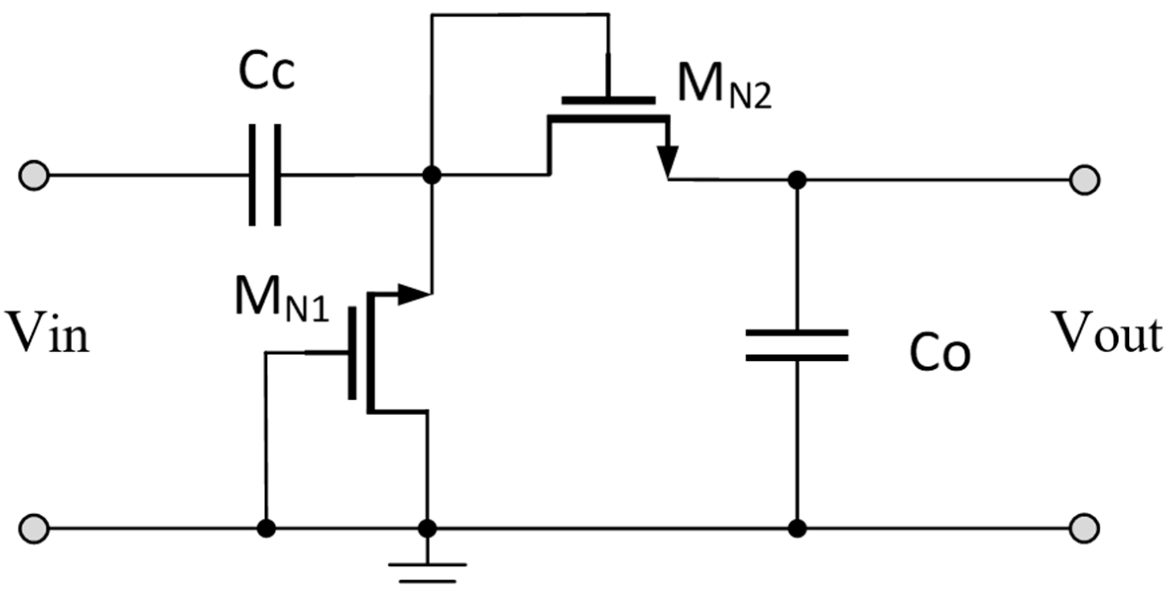
Among these components, the rectifier plays the most pivotal role in determining the system’s efficiency. Its performance governs the conversion of received AC power into usable DC power [
8]. One commonly used rectifier design is the Dickson’s charge pump model. This topology is particularly advantageous due to its simplicity and high voltage conversion efficiency.
Figure 2 illustrates the basic Dickson charge pump design, which comprises two diode-connected MOSFETs, a multiplying capacitor (Co), and a coupling capacitor (Cc) [
8].
The Dickson charge pump works in two different cycles. During the negative cycle of the input voltage, the MN1 transistor is turned on, and capacitor Cc is charged until the voltage across its terminals is equal to the input signal [
8]. The MN2 transistor is turned off since it is reversed-biased. During the positive half cycle, the MN1 transistor is reversed-biased and turned off. Transistor MN2 is forward-biased and turned on, while capacitor Cc starts to discharge. Capacitor Co starts to charge from the input signal and capacitor Cc [
8,
29]. The final output voltage is calculated from (1):
where
Vin is the input voltage and
Vth1 and
Vth2 are the threshold voltage of transistors MN1 and MN2, respectively [
29]. Finally, to achieve higher DC output voltage, the Dickson charge pump can be cascaded into multiple stages as needed.
A critical step in designing energy harvesting systems is the selection of the operating frequency band. This decision is influenced by the power density of available signals and the intended application of the energy harvesting system. The selected frequency band significantly impacts the design and size of system components, such as the antenna and rectifier, as well as the system’s overall performance [
8]. Consequently, optimizing the circuit for a specific frequency band is crucial to achieving efficient operation of the energy harvesting system. The most utilized frequency bands for energy harvesting are 900 MHz, 2.4 GHz, and 5.8 GHz. Lower frequency bands around 900 MHz are known for their ability to propagate over distances and their low power consumption, but they suffer from limited data transfer rates, making them less suitable for high-speed communication applications [
32]. Conversely, the 2.4 GHz band, widely used in Bluetooth and Wi-Fi devices, strikes a balance between range and data transfer capabilities, though it is prone to high interference [
33]. Meanwhile, high frequencies in the 5.8 GHz band are increasingly popular due to their numerous advantages. This spectrum supports the use of compact antennas, making it ideal for applications with space constraints [
34]. Furthermore, systems operating at 5.8 GHz provide an efficient power source, enhancing the connectivity and longevity of IoT devices [
27]. Energy harvesting systems at 5.8 GHz function effectively in diverse environments such as urban areas, industrial settings, residential spaces, and outdoor applications, including smart city infrastructure and public transportation systems [
32]. Additionally, they are effective in dense environments with high electromagnetic activity from wireless routers. Considering these aspects collectively shines a light on why employing the 5.8 GHz frequency is the best choice in energy harvester systems.
Despite these advantages, designing energy harvesting systems for 5.8 GHz poses unique challenges compared to lower frequencies. For instance, higher frequencies increase the effects of parasitic capacitance in circuits [
35]. This phenomenon is demonstrated in (2):
where
Xc represents the reactance and
f represents the frequency. As the frequency increases, the reactance decreases, allowing more current to flow. This reduced impedance significantly impacts circuit performance, often increasing leakage currents and energy losses.
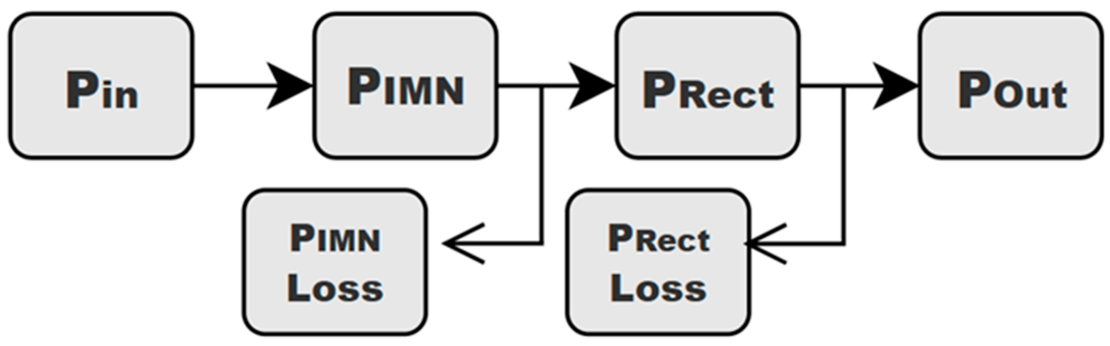
The performance of an energy harvesting system is primarily evaluated using metrics such as efficiency, sensitivity, and output power. The efficiency of an energy harvesting system is determined by the ratio of the DC output power to the RF input power. It is represented by the overall system efficiency as shown in (3):
where
ƞsystem is the overall system efficiency,
ηIMN is the efficiency of the impedance matching system,
ηRect is the efficiency of the rectifier, and
ηPMU is the efficiency of the power management unit. Among these, the efficiency of the rectifier is the most critical factor influencing system performance [
29].
In integrated circuit design at nanoscale dimensions, thermal fluctuations and energy dissipation play crucial roles in determining the performance and efficiency of rectifier circuits. These factors introduce parasitic effects, leakage currents, and resistive losses, which impact the overall power conversion efficiency (PCE) of the system. To account for these considerations, the efficiency of the rectifier can be rewritten as
where
PCE is the overall efficiency of the rectifier,
Pout is the output power converted,
Pin is the input power received by the system, and
PSE is the self-power loss of the switching element of the rectifier. Unlike conventional rectifier designs, which assume that fewer stages result in higher efficiency due to reduced power dissipation, a comprehensive design approach must consider additional factors, such as transistor sizing, forward voltage drop, on-resistance, junction capacitance, substrate parasitic capacitance, substrate leakage, and reverse leakage current.
In this work, the impact of entropy-driven energy losses and parasitic effects is mitigated through a combination of design optimizations:
Impedance matching: ensures high power transfer efficiency by minimizing reflection losses and voltage offsets.
Parasitic accounting: reduces bandwidth loss by carefully modelling and compensating for parasitic capacitances.
Minimizing current paths: limits leakage currents and resistive losses in the circuit layout.
Optimized metal routing and overlap: enhances layout efficiency by strategically overlapping metal layers and employing shielded routing to reduce parasitic resistance and undesired coupling effects.
By implementing these strategies, the proposed rectifier design effectively minimizes the inefficiencies introduced by nonequilibrium thermodynamics, thereby improving overall performance and maintaining a high-power conversion efficiency.
The rectifier’s power conversion efficiency (PCE) measures the effectiveness of converting RF power to DC power and is given by (5):
where
PCERect is the overall efficiency of the rectifier,
PDC Out is the output power converted, and
PRF In is the input power received by the system. The efficiency of CMOS-based rectifiers is often reduced by factors such as the threshold voltage drop across MOSFETs, power consumption by channel resistance, and substrate leakage [
36]. Enhancing rectifier efficiency requires reducing the threshold voltage drop in diode-connected MOSFETs.
The sensitivity of the energy harvesting system is the process of measuring the minimum required power to activate the system [
6]. The sensitivity is calculated in dBm using (6):
Since the AC received power is in the range of milliwatts or microwatts, the sensitivity is evaluated in dBm [
29]. One of the main approaches to increase the overall sensitivity is in the impedance-matching network [
6]. Precise impedance matching or tuning component values can help in increasing the sensitivity of the system.
The output power reflects the system’s ability to convert RF power into usable DC power. Monitoring and optimizing the output power at each stage of the energy harvesting system are essential for ensuring overall performance. A higher output power signifies a more effective energy harvesting process [
29].
Figure 3 illustrates the power flow within the system, emphasizing the importance of optimizing output power across all blocks.
3. Proposed Design
3.1. Simulation Model
The simulation process for the energy harvesting system is divided into two distinct phases. The first phase focuses on the design and simulation of the rectifier circuit at 5.8 GHz using the TSMC 65 nm process. This phase involves optimizing the circuit components to achieve enhanced performance at high frequencies. The TSMC 65 nm process was selected for this energy harvester design due to its excellent balance of performance, cost, and design flexibility. It offers low parasitic capacitance and leakage, minimizing unwanted interference and losses, which are critical for enhancing the overall efficiency of the energy harvester. Additionally, the process supports high switching speeds, which are essential for high-frequency applications. With a cost of $5800 per mm2, this process offers a cost-effective solution for subsequent production stages.
The second phase involves creating the layout of the designed rectifier circuit, followed by the extraction of the circuit from the layout. Once extracted, the circuit is thoroughly tested and analyzed to ensure that its performance aligns with the initial design simulations, thereby confirming the consistency of the design throughout the process.
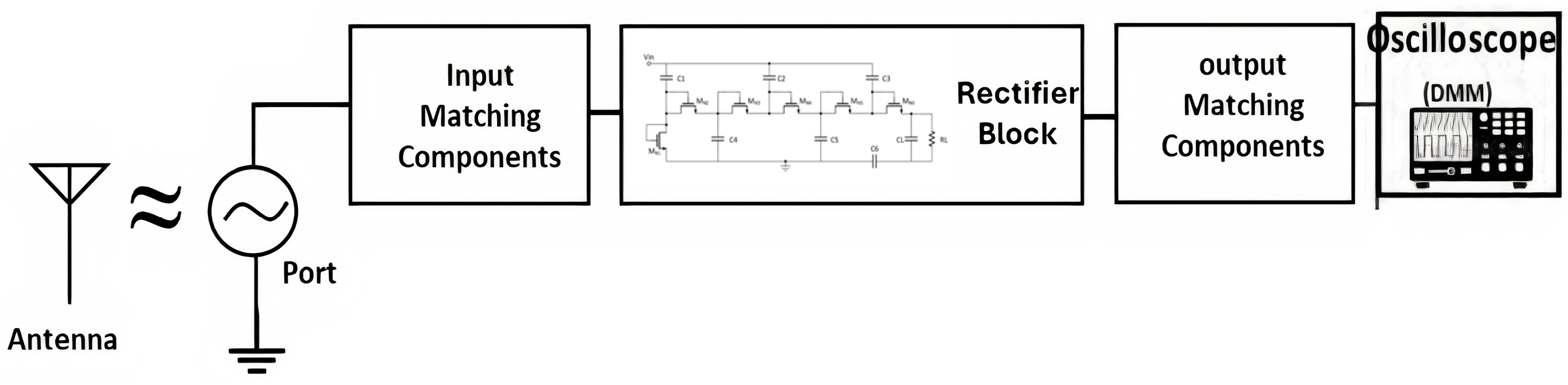
To emulate the real-world testing conditions during simulation, an antenna is replaced by an RF port of 50 ohm impedance, which is matched with the input impedance of the rectifier. At the output, the load (which is an oscilloscope) having a 50 ohm impedance is matched with the output impedance of the rectifier. The testing structure of the entire block is presented in
Figure 4.
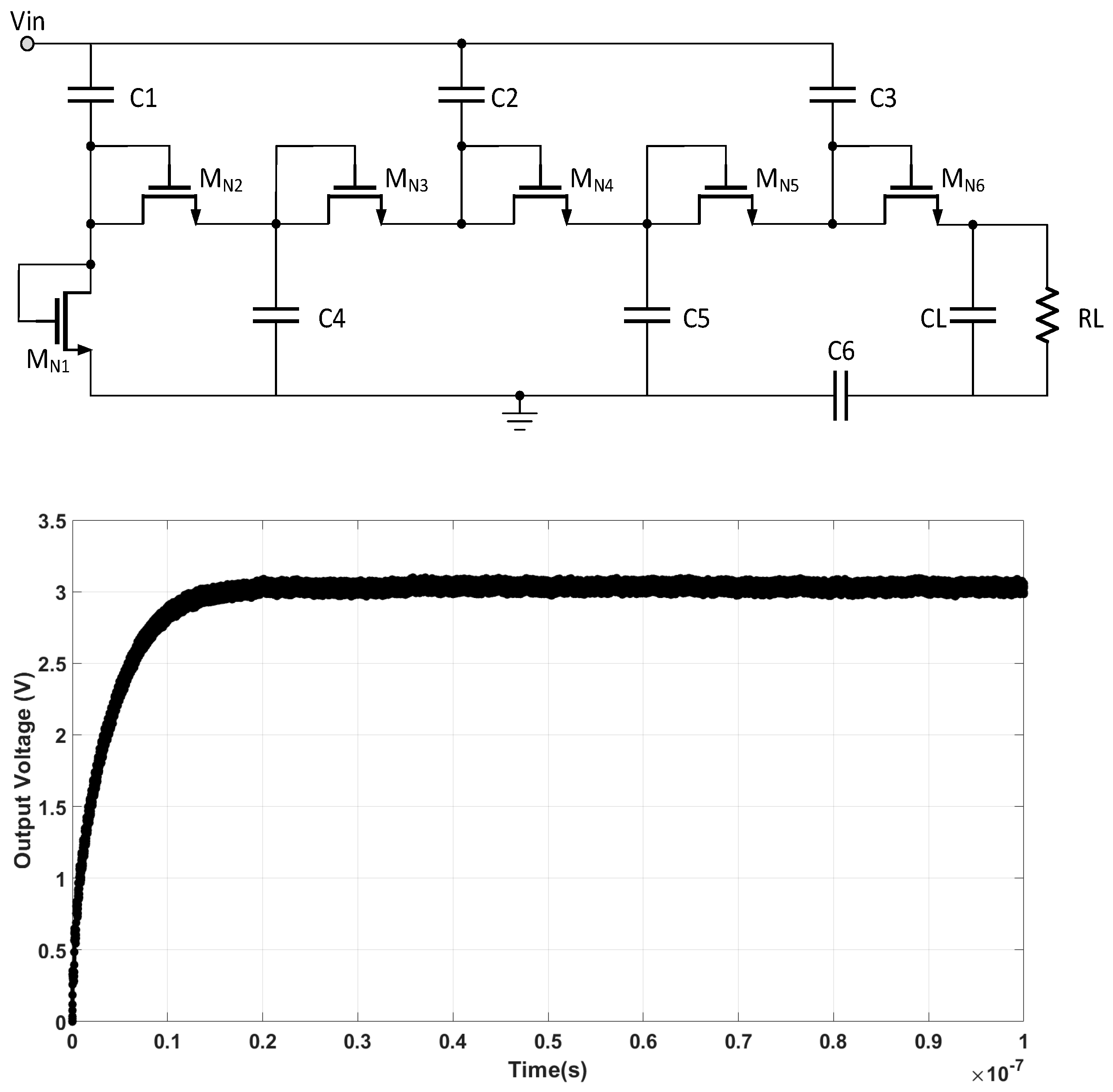
For the rectifier design, a three-stage Dickson charge pump is selected, as shown in
Figure 4. To enhance the performance of the original Dickson charge pump, an additional capacitor, C6, is integrated into the design. During the negative cycle, C6 is effectively disconnected because the MOSFET MN6 operates as an open circuit. This disconnection prevents stored charge from leaking through, thus reducing leakage current and improving the overall efficiency of the system [
8]. Furthermore, C6 plays a pivotal role in enhancing the output voltage by minimizing losses during the charging and discharging phases. Its inclusion ensures a higher sustained output voltage, which significantly contributes to the overall improvement of the system’s performance [
8].
To adapt the rectifier circuit for optimal operation at 5.8 GHz, the primary focus was on optimizing the output impedance for maximum rectification efficiency. This was achieved by systematically sweeping through various impedance values to identify the most effective one. The optimal output impedance was determined to be 10 kΩ. With this impedance value, the energy harvester rectifier, as depicted in
Figure 5, successfully operates at 5.8 GHz with minimal losses, achieving maximum efficiency and delivering an output voltage of 3 V.
To evaluate the performance of the 5.8 GHz three-stage rectifier, the total PCE is calculated. The input RF power is set to 0 dBm. The output DC power is determined using (7):
The total PCE is calculated using (5):
The simulation results demonstrate that the energy harvester achieves a high PCE of 90%, with an output voltage of 3 V. This indicates that 90% of the input RF energy is successfully converted into usable DC power with minimal losses. The output voltage of 3 V suggests that the harvester can provide a stable and sufficient power supply for low-power applications. The high efficiency and substantial output voltage highlight the effectiveness of the energy harvester in converting RF energy into usable power, making it well suited for powering IoT devices.
3.2. Layout Model
The layout process is a critical step in the design and verification of integrated circuits. It involves translating the circuit schematic into a physical layout, which is essential for manufacturing. This process includes the precise placement of transistors, resistors, capacitors, and the interconnection of these components using metal layers. The accuracy and efficiency of the layout directly influence the circuit’s performance, output power, and output voltage. Once the layout is created from the final circuit design, design rule checks (DRCs) and layout versus schematic (LVS) tests are performed to ensure the layout’s integrity and functionality. These tests verify that the layout adheres to the required design rules and matches the schematic representation, ensuring that the circuit operates as intended. The performance of the extracted circuit is then compared with that of the initial simulation to assess its output voltage and efficiency. This comparison provides a measure of the overall effectiveness of the design and its ability to meet the desired specifications.
To ensure the manufacturability, performance, and reliability of the extracted circuit, specific design requirements must be followed, which include the following:
The layout design process began with the individual creation of layouts for each MOSFET. Subsequently, all capacitors from the schematic were added to the layout and connected to their respective MOSFETs. Once all capacitors were placed and properly connected, the layout was finalized and prepared for testing, as shown in
Figure 6.
During the layout design process, a significant challenge emerged in optimizing the impact of extra resistors and parasitic capacitors, both of which play critical roles in the overall circuit performance. In integrated circuit layout design, the primary source of resistance comes from the metal tracks used for interconnections. The resistance of these metal traces can be expressed by (8):
where
is the resistivity of the material,
L is the length of the trace, and
A is the cross-sectional area of the trace. Increasing the cross-sectional area of the metal traces, by using wider or thicker traces, reduces the resistance. This reduction is advantageous because lower resistance results in reduced voltage drops, thereby improving the overall efficiency of the circuit. On the other hand, parasitic capacitors arise from the overlap between two different metal layers within the layout. These parasitic capacitors are represented by (9):
where
ϵ is the permittivity of the dielectric material,
A is the area of the metal plates, and
d is the distance between them. This increase in capacitance can lead to parasitic effects, such as slower rise times and degraded performance, particularly in high-frequency circuits.
The primary challenge in layout design lies in balancing the reduction of resistance with the control of parasitic capacitance. This trade-off has a significant impact on the circuit’s performance. While increasing the area of the metal traces reduces resistance, it simultaneously increases parasitic capacitance due to the larger overlap between adjacent metal layers. This results in capacitive coupling, which can adversely affect the circuit’s frequency response and stability. Achieving the optimal balance between these two factors is essential. This can be accomplished through careful material selection and the implementation of smart layout techniques, such as maintaining appropriate spacing between metal layers to minimize overlap and parasitic effects. By optimizing the layout to manage these factors effectively, the circuit’s performance can be enhanced, ensuring both low resistance and minimal capacitive interference.
In the long-term usage of the energy harvester, the parasitic capacitance and resistance may change due to environmental factors such as temperature variations, aging effects in the semiconductor materials, and process-induced variations. These factors can lead to performance degradation over time, emphasizing the need for robust design considerations to ensure long-term stability [
35]. Variations in dielectric properties can modify the effective capacitance values, potentially shifting the impedance-matching conditions. This shift can reduce power transfer efficiency and alter the resonant frequency of the harvester, affecting the rectifier’s ability to efficiently convert RF energy [
35]. Additionally, aging effects in metal interconnects and semiconductor junctions can lead to increased resistive losses, thereby reducing overall efficiency. Higher resistance in the layout metal traces can introduce additional voltage drops, further impacting the PCE and overall performance stability of the energy harvester.
Energy harvesting efficiency is greatly influenced by entropy generation and thermodynamic losses. Excessive entropy generation in electronic components causes heat dissipation, increased interconnect resistance, and inefficiencies in charge transfer, all of which degrade long-term performance [
38]. In high-frequency energy harvesters, thermal management becomes especially important to minimize these losses and maintain stable energy conversion. Thermodynamic analysis of these systems reveals that outgoing thermal radiation imposes constraints, making it clear that optimized design strategies are needed to enhance efficiency [
39]. Additionally, entropy-based reliability analysis provides insights into how heat buildup affects both material properties and the longevity of devices [
38]. Proper heat management can prevent material degradation and reduce the risk of failure. To achieve long-term stability, it is essential to optimize both the thermal and electrical characteristics of the rectifier circuit. Theoretical models further show the maximum efficiency that can be achieved in energy conversion, emphasizing the need to minimize entropy generation to avoid performance loss [
39]. By addressing these factors through careful design, energy harvesters can maintain efficiency over extended periods.
To mitigate these effects and ensure long-term performance stability, the following design strategies are implemented:
Low-resistance metal routing: wider metal traces are used in critical paths to minimize resistive degradation and improve long-term reliability.
Temperature variations: the circuit is simulated across a range of temperature variations to ensure stable operation under different environmental conditions.
Use of low-threshold voltage transistors: low-threshold voltage transistors are used to enable larger channel lengths which minimize leakage currents while maintaining efficient charge transfer.
Impedance-matching network design: the impedance-matching circuit can be designed with a margin to accommodate minor variations in parasitic capacitance, ensuring stable power transfer over time.
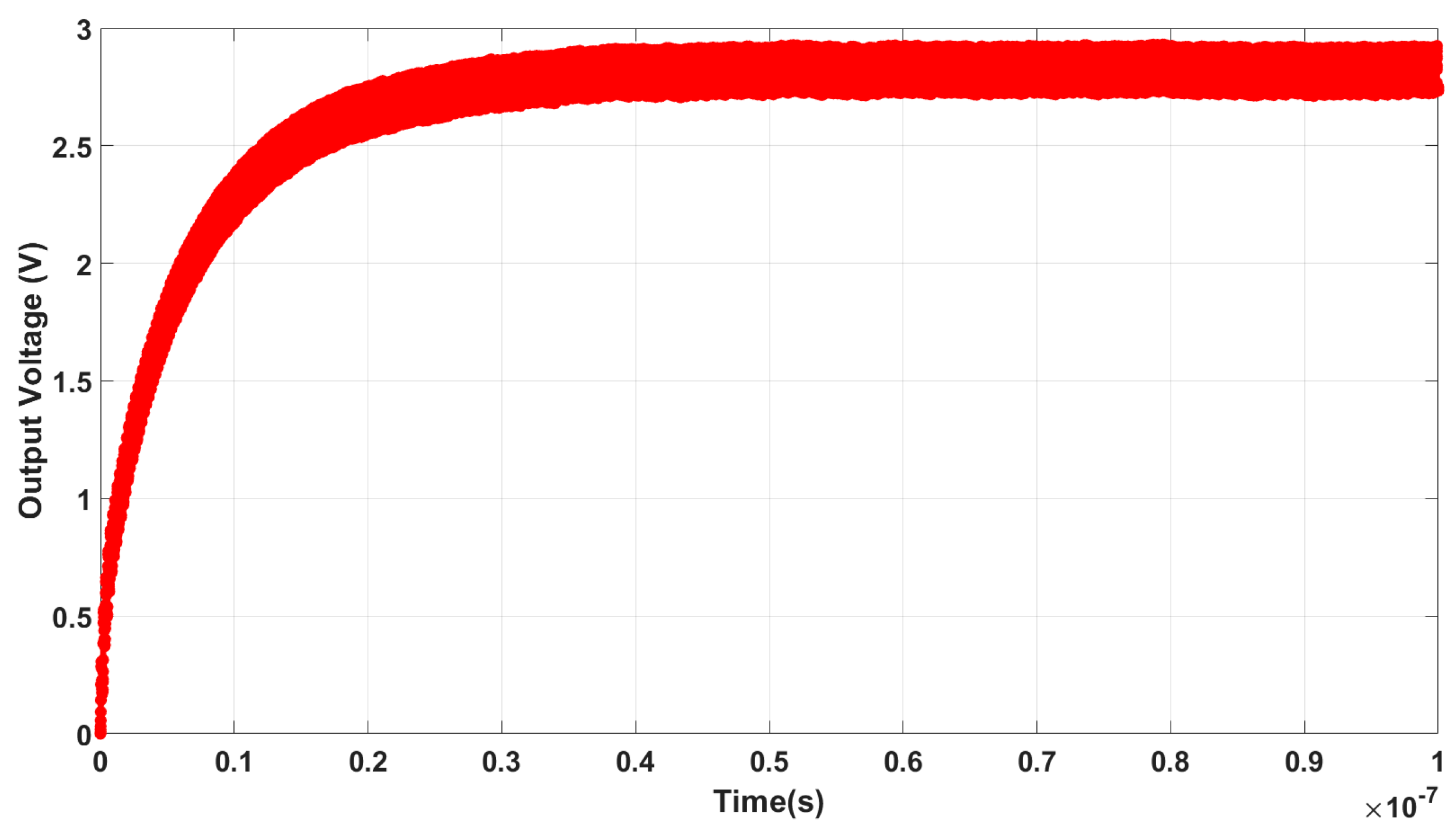
The primary tests performed on the layout circuit are the design rule check (DRC) and layout versus schematic (LVS). The DRC is an essential verification step in integrated circuit design, ensuring that the layout complies with the design rules specific to the fabrication process. These rules address critical parameters such as spacing between components, the overlap between different metal layers, and the minimum width of metal traces. Strict adherence to these design rules is crucial for preventing manufacturing defects and ensuring the reliability of the final circuit. The LVS test, on the other hand, verifies that the physical layout accurately reflects the intended schematic design. This test ensures that all connections and components are correctly implemented in the layout, helping to prevent potential functional discrepancies between the layout and the original design. The design successfully passed both the DRC and LVS tests, and a circuit was extracted from the layout, showing the addition of parasitic components. To assess the impact of the additional components, the output voltage of the extracted circuit was simulated, as shown in
Figure 7, which demonstrates an average output voltage of 2.88 V.
To further evaluate the performance of the extracted circuit, the power conversion efficiency (PCE) is calculated as follows.
The output DC power is determined using (7):
Using the calculated output power, the total PCE is determined using (5):
This calculation shows that at a frequency of 5.8 GHz, approximately 83% of the RF input power is successfully converted into DC output power. This high efficiency indicates that, despite the presence of parasitic elements introduced during the layout process, the circuit remains highly effective in harvesting and converting RF energy. The minimal losses reflect the optimized design of the rectifier, ensuring that a significant portion of the input power contributes directly to the desired DC output, making it suitable for energy harvesting applications at high frequencies.
4. Performance Comparison
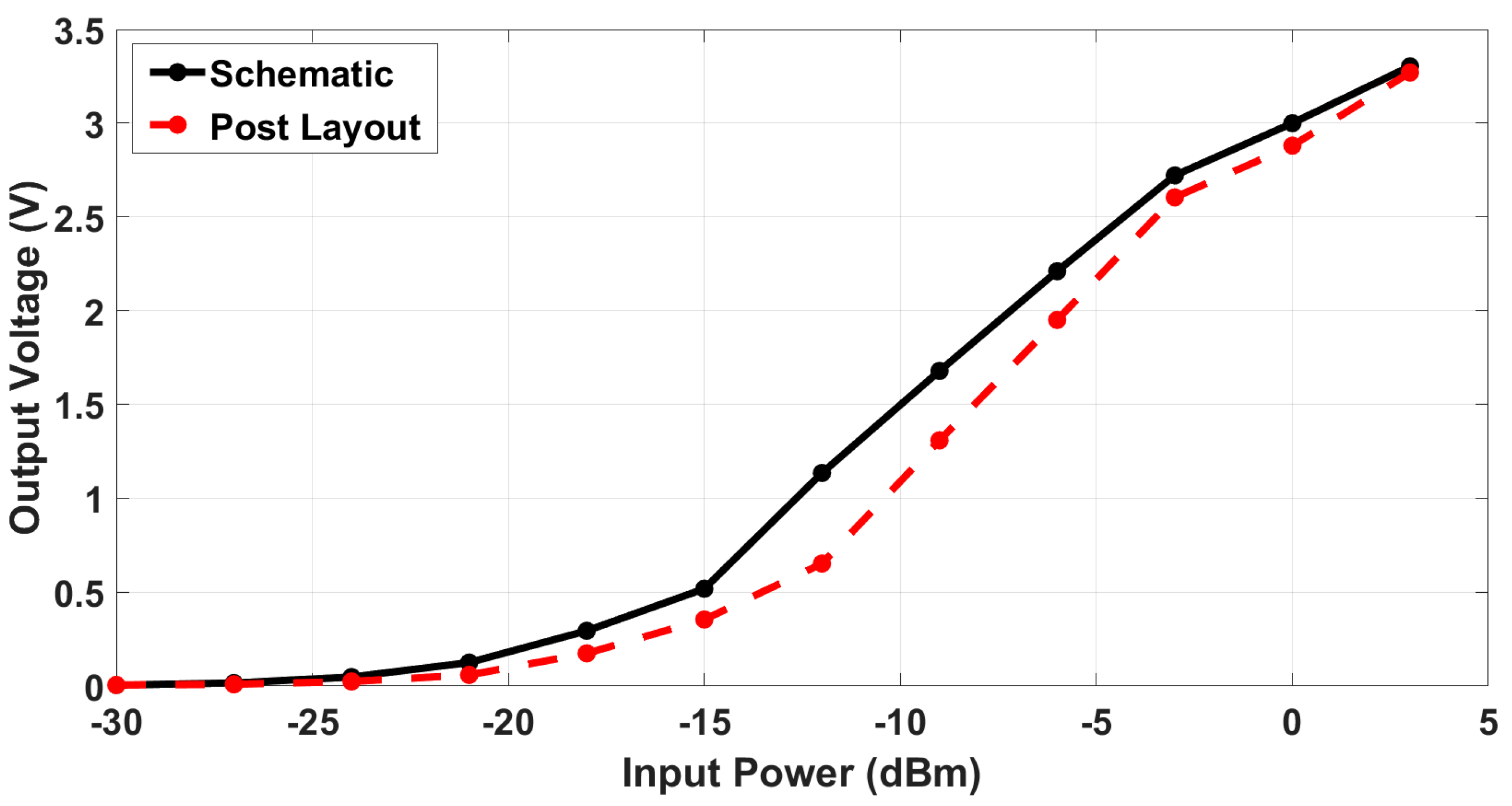
To evaluate the accuracy of the layout-extracted circuit, the output voltage of both the simulated and extracted circuits is analyzed. While the output voltage remains largely consistent when comparing the simulated results to those of the extracted circuit from the layout, there is a slight reduction in performance. The average output voltage for the simulated circuit is 3 V, whereas the extracted circuit averages 2.88 V. This minor difference is attributed to parasitic capacitance introduced during the layout stage. Although the simulated results show a stable output voltage with minimal variation, the extracted circuit exhibits more ripple, indicating that its performance is slightly less smooth. The most notable difference between the two waveforms is the increased ripple in the extracted results, which can be attributed to parasitic components such as capacitances and resistances introduced during the layout process. These parasitic elements, including capacitors formed by the overlap of metal layers, lead to unwanted capacitance in the circuit, causing instability and oscillations, which manifest as ripples. Additionally, resistive losses from the metal interconnects can introduce voltage drops, further contributing to irregularities in the output signal. This demonstrates that the extracted circuit contains parasitic resistances and capacitances that were not present in the ideal simulation. These layout-extracted parasitic resistances cause the circuit’s performance to diverge from the ideal simulation. As a result, the extracted view provides a more realistic representation of the physical chip’s performance under real conditions.
The performance of the energy harvester circuit is evaluated further under various conditions, including input power and temperature, for both the simulated and post-extracted circuits. The output voltage of the energy harvester circuit was observed for different input power levels.
Figure 8 provides a comparison between the simulated and post-extracted output voltages versus input power. In both cases, the circuit performs efficiently across a wide range of input power levels. As expected, the output voltage increases with rising input power. However, the post-extracted circuit shows slightly lower voltages compared to the simulated circuit. This reduction in performance can be attributed to parasitic resistances and capacitances introduced during the layout extraction, which causes a slight degradation in the post-extracted circuit. The parasitic elements, including those from the interconnects and metal layer overlap, lead to energy losses and reduced efficiency, which explains the observed voltage drop in the post-extracted results.
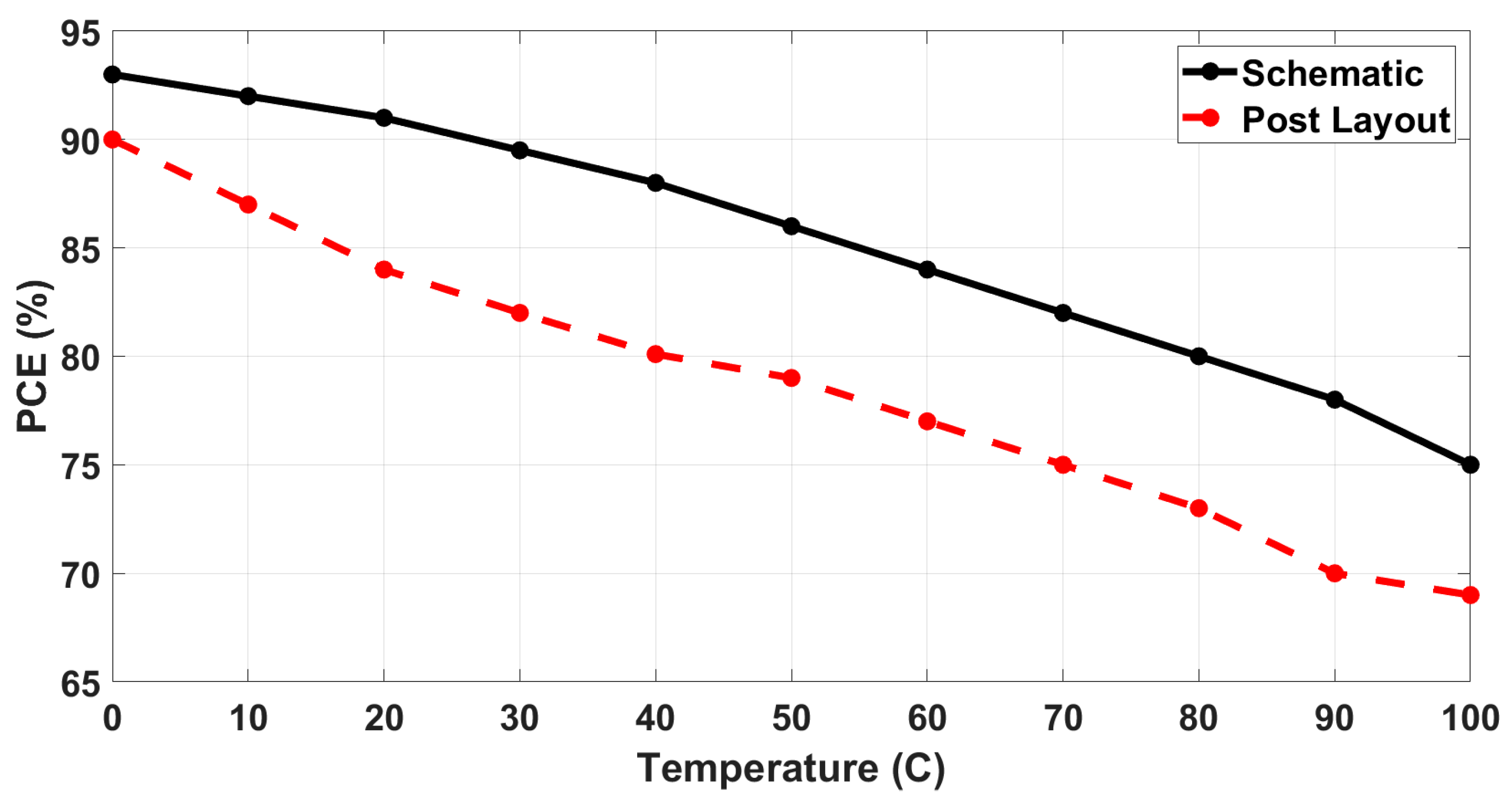
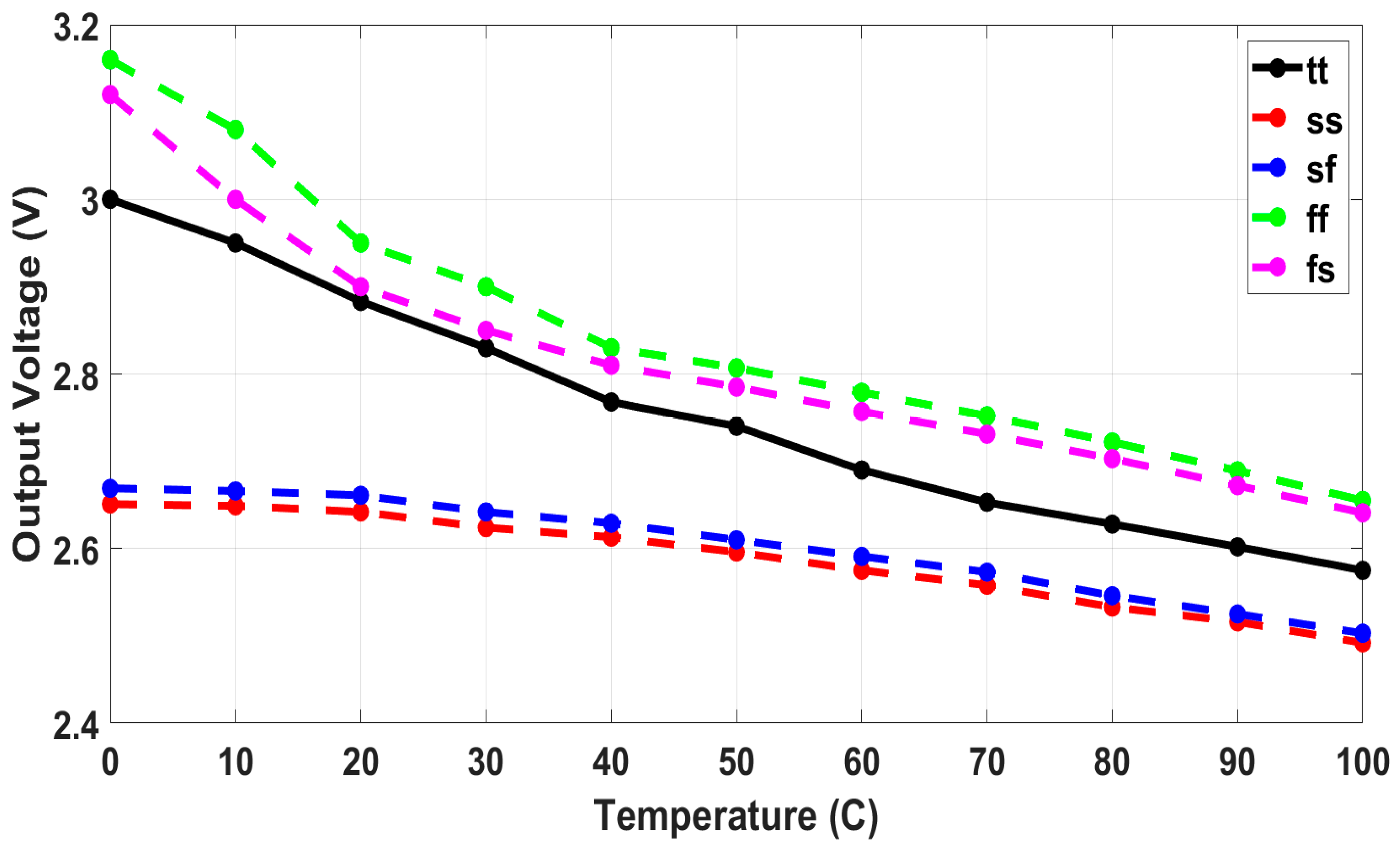
The effect of temperature on the output voltage was also examined. The output voltage was monitored across a range of temperatures from 0 °C to 100 °C, as shown in
Figure 9. In both the simulated and post-extracted circuits, the output voltage decreases as the temperature rises. This trend is expected due to the temperature-dependent behavior of semiconductor devices, where an increase in temperature typically leads to higher leakage currents and a reduction in overall performance. The PCE was also evaluated across the same temperature range, as shown in
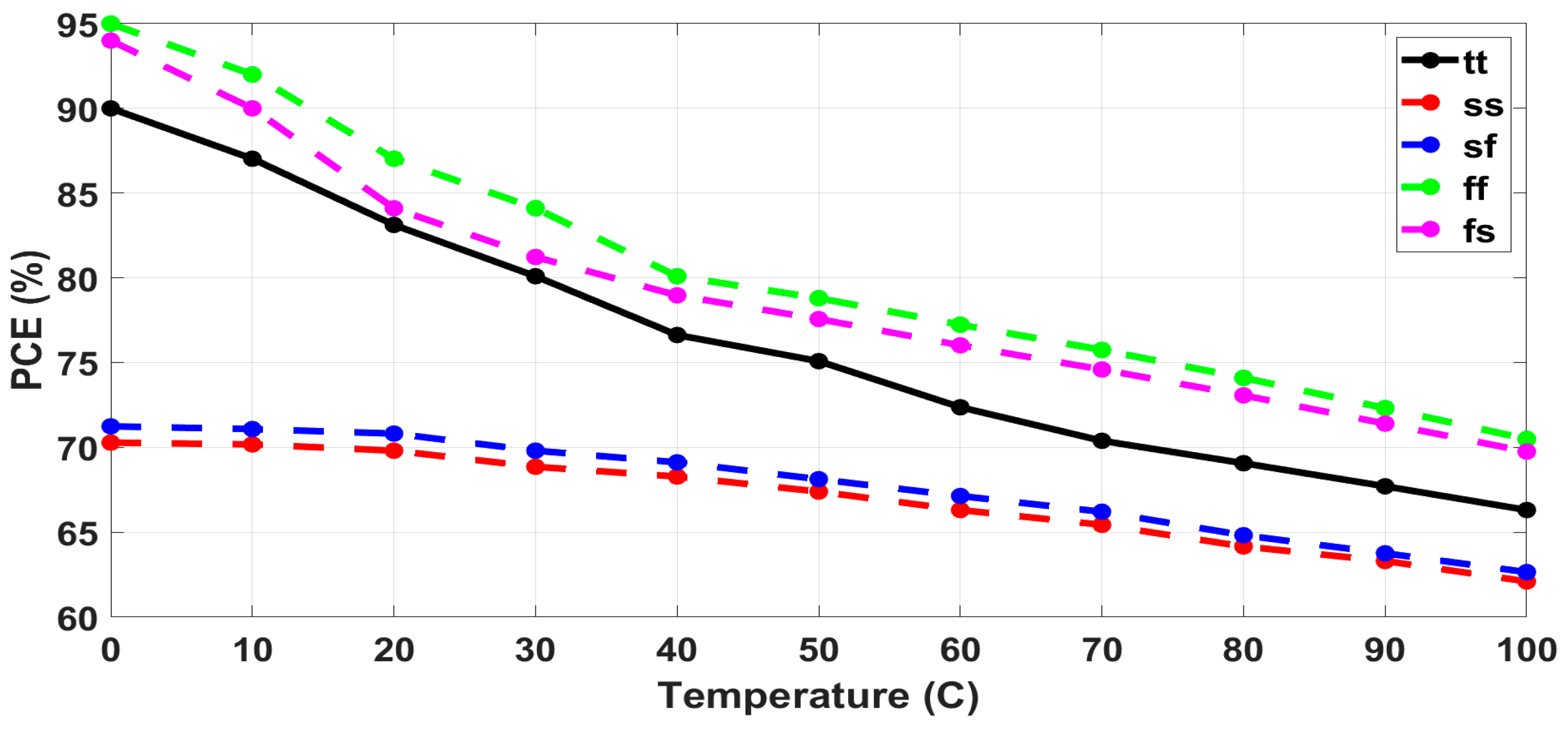
Figure 10. In both the simulated and post-extracted circuits, PCE decreases as the temperature rises, which is consistent with the general behavior of rectifier circuits at higher temperatures. The drop in the output voltage and the PCE can again be attributed to the presence of parasitic elements introduced during layout extraction. The output voltage and the PCE of the post-extracted circuit show a more rapid decline with increasing temperature compared to the simulated circuit, indicating that the circuit’s performance is more impacted by parasitic effects introduced during the layout process, making it more sensitive to temperature variations.
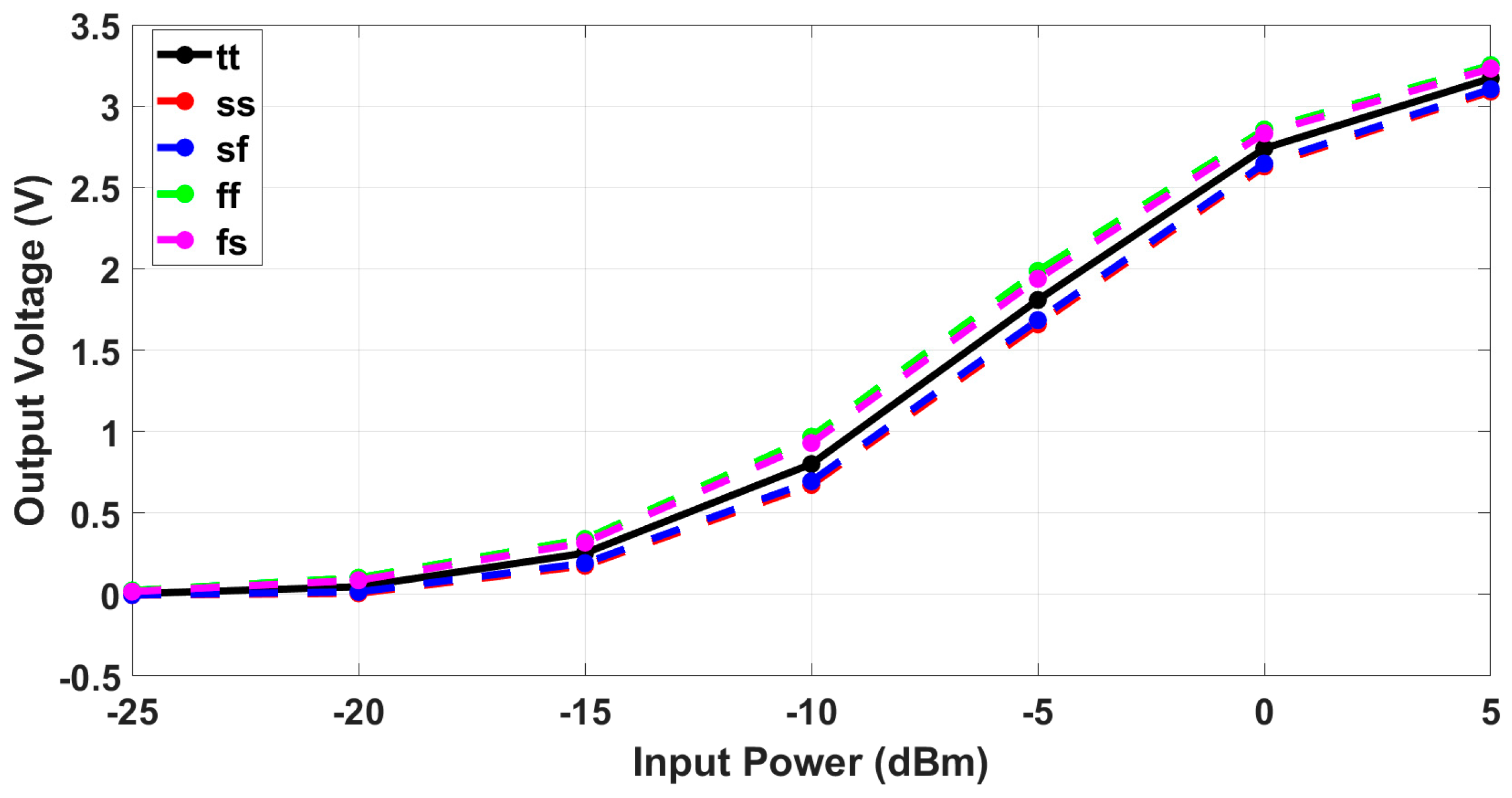
The achieved output voltage and PCE are suitable for powering low-energy IoT devices, making the designed rectifier highly efficient for energy harvester systems. To ensure that the designed energy harvester will operate in the same way after fabrication, it is imperative that a rigorous functionality check is carried out across process corner variations.
Figure 11 shows the output voltage vs. input power behavior across five available process corner variations, mainly typical (TT), fast (FF), slow (SS), slow–fast (SF), and fast–slow (FS).
It can be seen from the graph that the performance of the designed harvester does not degrade across process corners, and it matches the behavior, as shown in
Figure 8. Furthermore, the designed circuit was simulated across the five process corners to assess the functionality of the output voltage at varying temperatures.
Figure 12 presents the variations of output voltage across the temperature range of 0 to 100 degrees. As can be seen by the graph, the best performance is achieved at the FF and FS process as the value of the threshold voltages is lowest during those processes. The worst performance, which, however, is still sufficient, is seen in the SS and SF process corners as they have highest threshold voltages. It can be deduced that the designed chip will work efficiently even if it is fabricated under different process corners.
To further verify the performance of the circuit, PCE was simulated across the temperature range of 0 to 100 degrees across the five process corner variations. As can be deduced from the graph (
Figure 13), the best expected results are achieved at the FF and FS processes, and the worst are achieved at the SS and SF processes (which, however, are still in the acceptable range).
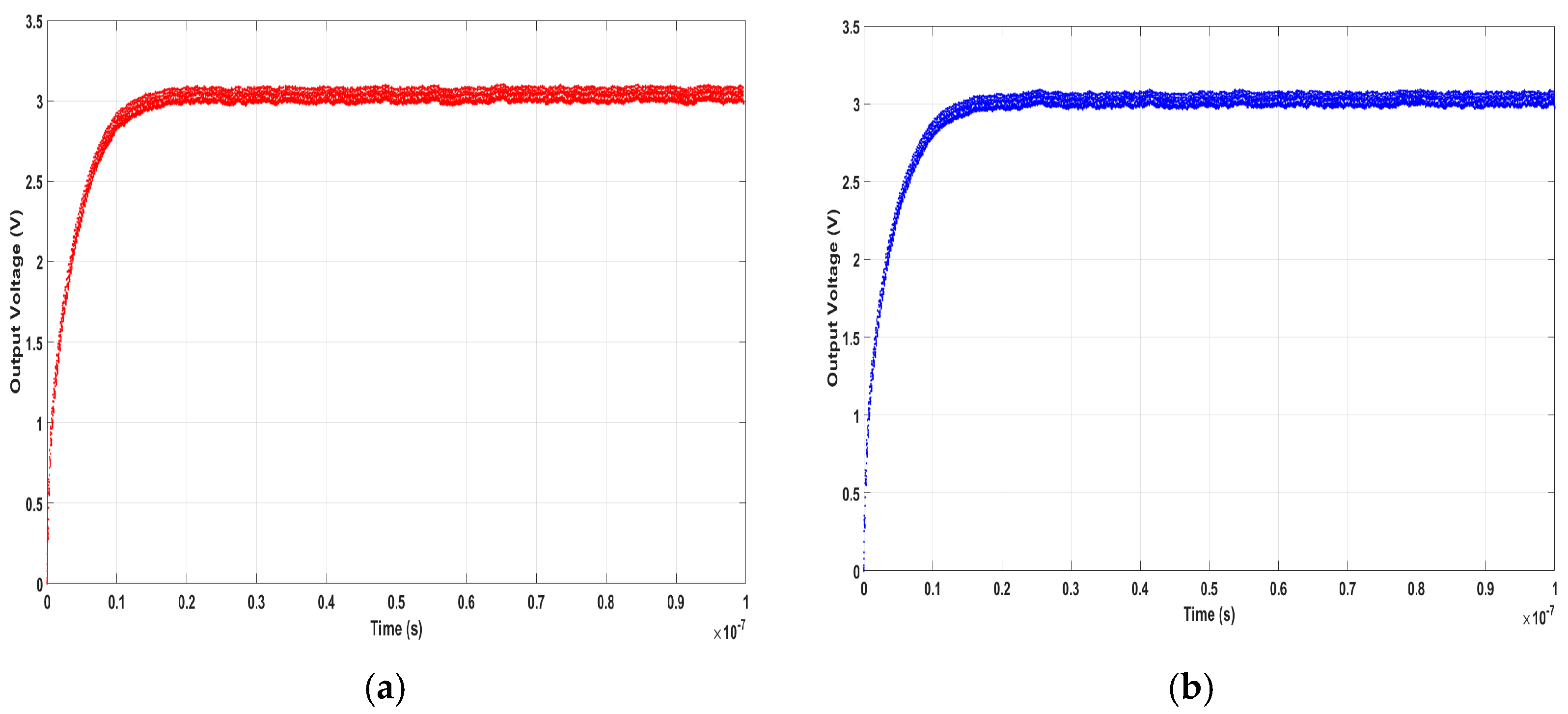
Further simulations were performed on the circuits imitating the Monte Carlo type of simulations, in which the width, length, and the threshold voltage of the transistors are varied to their maximum and minimum values, as provided in the PDK of the process.
Figure 14 presents the output voltage of the extracted energy harvester circuit, in which (a) represents the minimum possible width and (b) depicts the maximum possible width of the transistors used in the circuit design.
Figure 15 shows the variations of output voltage with minimum (a) and maximum (b) length as provided in the PDK. It can be inferred from the results that the output voltage does not degrade and still behaves in a similar fashion when the width and length of the transistors are varied even though the threshold voltage is dependent on these two parameters of the transistors.
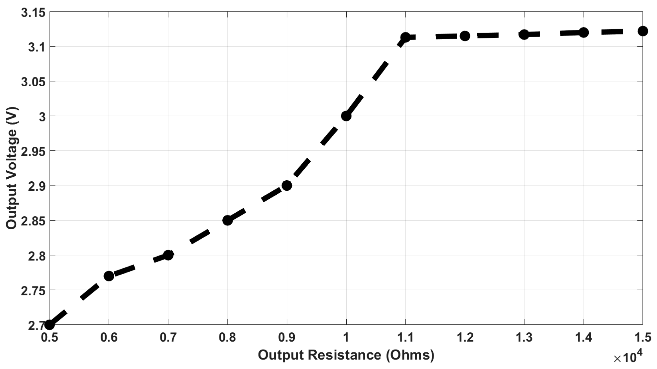
Figure 16 depicts the output voltage curve with respect to the changes in the load-resistance values. From the graph, the maximum voltage is obtained at 10 KΩ of load resistance.
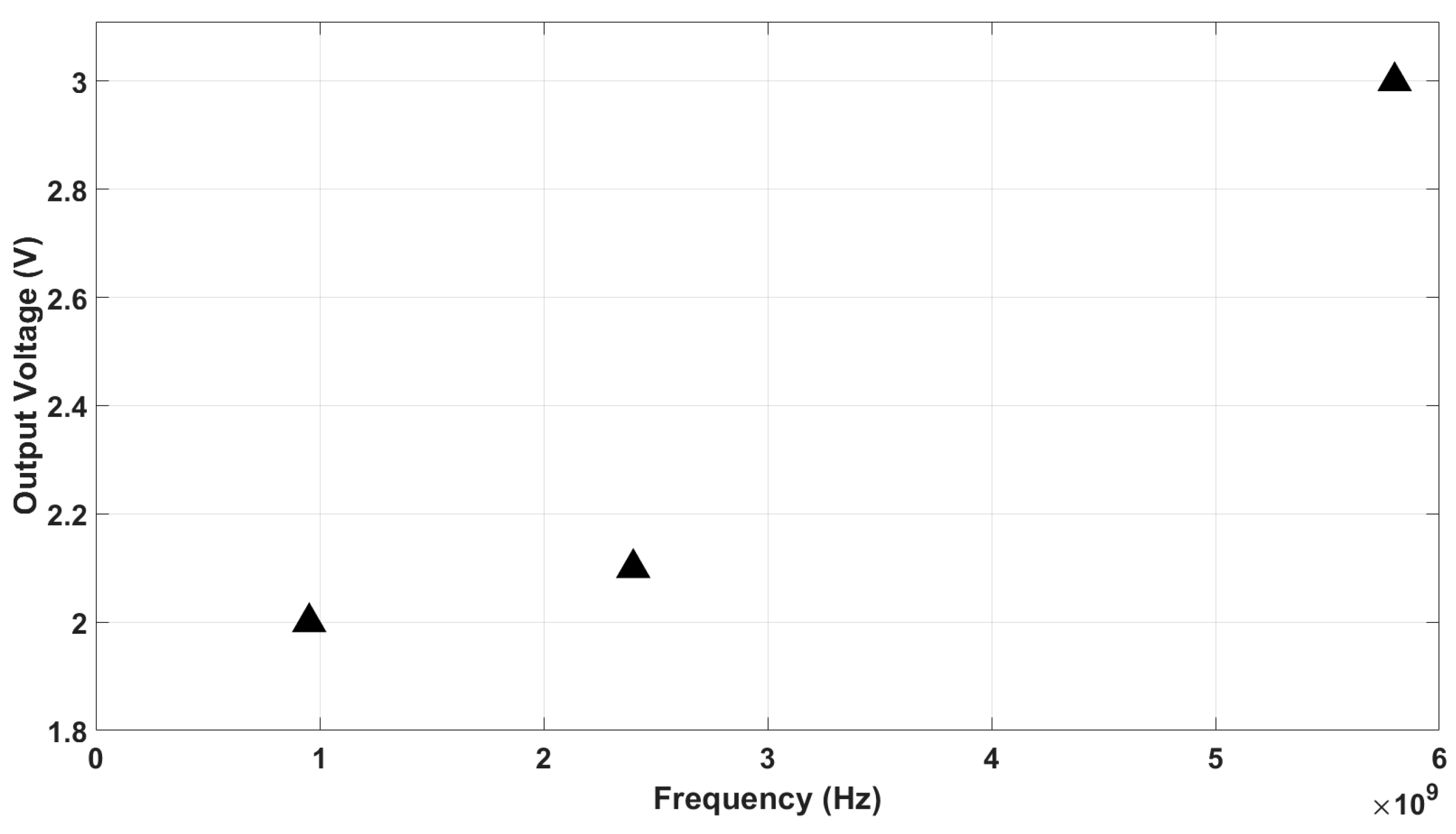
Figure 17 shows the performance of the rectifier output voltage at three different input frequency bands (953 MHz, 2.4 GHz, and 5.8 GHz). As can be seen from the graph, the maximum output voltage is obtained at 5.8 GHz as the rectifier’s input impedance is matched to the source output impedance (antenna) at 5.8 GHz, thus ensuring maximum power transfer at that particular frequency.
Table 1 summarizes a comparison between the performance of this work and the performance of rectifiers mentioned in the literature review. It is shown that for a frequency of 5.8 GHz, the rectifier designed in this work achieves the highest efficiency. This demonstrates the effectiveness of the design in harvesting energy at higher frequencies, especially compared to similar works operating in the same range. This comparison highlights the potential of this rectifier design for use in real-world applications.


