Abstract
Megahertz switching frequencies in converters significantly reduce the size of passive components, enabling high power density. However, these frequencies also introduce operational challenges, such as the semiconductor device reliability, thermal management, magnetic design and electromagnetic interference. This paper discusses a dc-dc converter operating at 1 MHz and its associated design challenges. The relationship between a GaN device on-resistance, junction temperature and losses in scenarios where the converter operates beyond its nominal design specifications is analyzed. Additionally, a PCB-based inductor is fully characterized and the parasitic effects of PCB traces are examined for a 1-MHz, 1-kW application. Finally, the conducted and radiated emissions of the converter are addressed, supported by simulation and hardware experimental measurements.
1. Introduction
Power electronic converters have become an integral part of various applications including aerospace applications, electric ships and electric vehicles [1]. In these applications, highly power-dense, efficient converters are desired to reduce the empty weight of the electrified transportation and increase the payload. To meet these stringent requirements, switching frequencies are being pushed into the megahertz (MHz) range to reduce the size and weight of passive components [2]. Higher frequencies can reduce the passive component size but pose challenges such as the semiconductor reliability, thermal management, magnetic design and electromagnetic interference (EMI) [3].
The advancement of wide bandgap semiconductors has profoundly influenced converter design paradigms by enabling operation at higher switching frequencies [4]. A key challenge is the fluctuating drain-to-source on-resistance, , in Gallium Nitride (GaN) devices under varying load conditions [5]. Traditional conduction loss estimations rely on static values, often neglecting dynamic behavior in harsh operating conditions [6]. Accurately predicting the junction temperature, , at MHz frequencies and kilowatt power levels is crucial to prevent device degradation [7]. Various methods have been proposed to measure the dynamic , such as on-chip measurements using specific chip designs [8] or supplemental circuitry near the GaN device [9], but these are often complex or application specific. While effective at lower frequencies or power levels, these methods can negatively impact the GaN device performance at MHz frequencies and kilowatt power levels.
Despite the benefits of higher frequencies, magnetic components remain a bottleneck for further advancements [10]. PCB-based magnetics are widely adopted in MHz power converters due to their ease of manufacturing and consistent quality [11]. However, the parasitic capacitance in multilayer structures can degrade performance and contribute to common mode noise as the frequency and power levels increase [12]. While PCB-based inductors parasitic capacitance has been studied, most works focus on kHz-range switching frequencies [13] or MHz designs limited to a few hundred watts [14]. Likewise, a planar inductor for a 300 kHz, 2.7 kW converter was investigated [15], but parasitic behavior was not analyzed, leaving gaps in the understanding of its impact on higher power designs.
Another major challenge in MHz designs is EMI, which becomes increasingly significant as both the frequency and power levels in the converter rise [16]. The root causes of EMI often stem from PCB parasitics in the layout, mainly due to large critical loop areas. Poorly designed layouts in higher frequency circuits introduce parasitic inductances, causing voltage and current overshoots that lead to EMI [17]. Additionally, switching oscillations, particularly in wide-bandgap devices, contribute to EMI and require proper mitigation techniques [18]. The existing studies on EMI typically focus on power converters operating at kilohertz-range frequencies [19,20].
Figure 1 provides a visual representation of the key areas addressed in this paper, where Figure 1a illustrates the converter used in this study. It shows the GaN High-Electron Mobility Transistor (HEMT) device and the thermal network used to establish the relationship between and . It also highlights the loop inductances, , which are a major source of voltage and current overshoots/ringing and EMI. Figure 1b depicts the parasitic effects in the inductor, and Figure 1c illustrates the EMI spectrum found in a converter. The contributions of this work build upon the aspects shown in Figure 1:
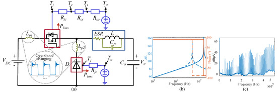
Figure 1.
(a) Buck converter illustrating loop parasitic effects, featuring GaN HEMT and Silicon Carbide Schottky diodes along with thermal networks used to establish relationship between , and associated losses. Other critical challenges include (b) inductor parasitic effects and (c) EMI.
- 1.
- A linear equation was formulated to model the dynamic of the GaN device as a function of the losses and , with its performance analyzed under MHz operation across varying load conditions.
- 2.
- A 1-MHz, 1-kW PCB-based inductor was characterized using simulation and hardware measurements to evaluate the parasitic capacitance effects at higher frequency and kilowatt power levels.
- 3.
- The conducted EMI in a MHz buck converter was analyzed through simulations with radiated EMI measured in a hardware setup, providing insights for future MHz designs.
The rest of this paper is organized as follows. Section 2 presents the methodology developed to study the three key challenges associated with higher power and frequency converter designs identified in this research. Section 3 provides the simulation results, followed by a discussion of the experimental results in Section 4.
Section 5 concludes the article.
2. Methodology
This section outlines the methodology for studying the operational challenges of the MHz buck converter shown in Figure 1a. It covers the development of the equation, the magnetic material selection and the PCB-based inductor design and EMI. The converter design specifications are listed in Table 1.

Table 1.
Buck converter design specifications.
2.1. GaN HEMT Dynamic On-Resistance ()
In power converters, both the conduction and switching losses are key factors affecting the temperature of the switching component [21]. The conduction loss depends on the of the device. This resistance tends to increase during long term operation due to charge trapping during high-voltage off-state biasing caused by the electric field, electron-induced charge trapping during hard-switching, and a rise in the [22]. An increase in leads to higher conduction losses in switching devices, which in turn raises the . Higher switching frequencies lead to more stress on the device and are a reason for faster degradation. Therefore, understanding the behavior of is crucial with respect to extreme conditions of overloading for achieving the efficient thermal management and reliability of these devices.
To account for these dynamic load conditions and to study the behavior, a linear equation was developed using the normalized curve for provided by the manufacturer to calculate the normalized on-state resistance , based on the , as
where a and b represent polynomial best fit constants with values of 0.008663 and 0.7653, respectively. It should be noted that these constant values are suited only for the GaN device used in this paper. After finding , the operational calculated on-state resistance is given as
where is the value provided in the datasheet by the manufacturer. The experimental measurement of is challenging in a packaged die; therefore, a thermal model should be used to calculate , which is dependent on the total power losses. These losses are the switching losses, , and conduction losses, . The switching losses depend mainly on the switching frequency of the device, , and can be calculated as
where is the input voltage, is the output current, is the rise time and is the fall time. The conduction losses are affected by and the current through the device, , and are calculated as
Finally, the total power losses, , are calculated by combining and as
After calculating the total losses, a thermal network is used to estimate the temperature behavior. The use of a thermal network allows for the accurate representation of the thermal behavior of MOSFETs and heatsinks [23,24]. The thermal resistance information for this model was obtained from the datasheets of the GaN device, heatsink and thermal pad. Additionally, a safety margin of 10% was incorporated into the thermal resistances of each medium to account for potential variations and uncertainties. The thermal network of the switch is illustrated in Figure 1a. signifies the case temperature, represents the heatsink temperature and corresponds to the ambient temperature. The thermal resistances include the junction-to-case, , case-to-heatsink, , and heatsink-to-ambient resistances, [25]. From the thermal network, can be calculated as
As the device operational lifetime decreases, progressively increases. To further investigate the dynamic model, a special case study was conducted where the converter operated beyond the nominal design specs.
2.2. Core Material Selection and PCB-Based Inductor Design
There are limited options for magnetic materials at MHz and higher frequencies. Magnetic materials such as 3F36 are well suited for frequencies below 1 MHz, while alternatives such as 3F4 and 3F46 can effectively operate up to 3 MHz [26]. The ferrite material 3F4 was chosen due to the low power loss characteristics at a nominal operating frequency for this design and the availability of the selected core shape and size in the market. The planar core shape (E43/10/28) was selected to match the PCB inductor winding dimensions and the core window area.
The inductor design required five turns to achieve the desired inductance. Two approaches were evaluated: the first involved placing three turns on the top layer and two turns on the bottom layer with a copper thickness of 1 oz, while the second placed all five turns on the top layer with a copper thickness of 2 oz. The width of the copper traces on the PCB was determined based on the inductor current requirements of the 1 MHz buck converter.
A square geometry was chosen for the inductor, as shown in Figure 2, where is the outer diameter, is the inner diameter, s is the distance between two adjacent turns and w is the thickness of the trace width [2].
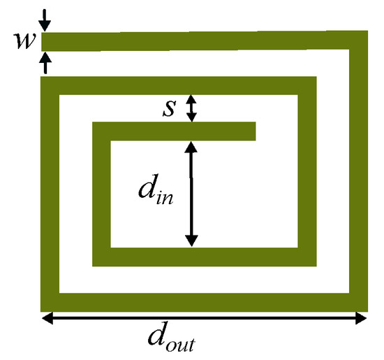
Figure 2.
PCB−based inductor geometry.
2.3. Electromagnetic Interference (EMI)
EMI in power converters is categorized into two primary types: conducted and radiated. Conducted EMI is further subdivided into differential mode and common mode EMI [27]. Both differential mode and common mode noise travel through the main power lines and distort the signal waveforms. Common mode noise couples through the parasitic capacitance via the chassis ground of the converter unit and flows back to the converter. In contrast, the primary sources of radiated EMI are high current loops and high nodes [28].
The conducted EMI was analyzed using Finite Element Analysis (FEA) and electrical simulation tools, while the radiated EMI was tested on hardware. The EMI results were evaluated in accordance with electromagnetic compliance standards, specifically the International Special Committee on Radio Interference (CISPR) guidelines. CISPR 32 was applied to the conducted EMI, while the radiated EMI testing followed CISPR 25 [16].
The conducted EMI was analyzed using two approaches. First, the PCB layout was designed and PCB parasitics such as the inductance were extracted using FEA. These extracted parasitics were subsequently modeled in power electronics-focused circuit simulator software, SIMPLIS. The co-simulation workflow is shown in Figure 3a. After designing a prototype layout, the PCB files were imported into SIwave. Then, the PCB scattering, admittance and impedance (SYZ) parameters were computed for post-EMI study. These parameters describe the electrical behavior of a linear electrical network [29]. In SIMPLIS software, a Line Impedance Stabilization Network (LISN) model was developed to differentiate between differential-mode and common mode emissions.
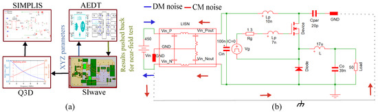
Figure 3.
Setup for conducted EMI (a) FEA co−simulation flow [29] and (b) LISN model with buck converter showing differential mode (DM) and common mode (CM) noise flow.
Figure 3b shows the simulation setup for the conducted EMI in SIMPLIS. To visualize common mode noise, a small parasitic capacitance, , was introduced to mimic the capacitance from the heatsink to the chassis of the actual converter as a primary source of common mode noise coupling. The LISN model was employed to simulate the electrical model of the converter.
3. Simulated Results
This section outlines the simulation setup used to study the operational challenges of the MHz converter. It includes details on the tools employed and discusses the simulation outcomes.
3.1. Case Study of GaN Device On-Resistance at Beyond-Nominal Operation
The converter PCB was designed for a maximum current rating of 6.5 A and nominal operation of 5.5 A. During testing, the load profile changes in steps, with each step change occurring after a steady-state wait time, were observed.
Figure 4 shows the on-resistance calculated using the method mentioned in Section 2.1 during converter operation at varying loads. The calculated was normalized against the specified in the manufacturer datasheet. Here, 1 per unit represents the nominal operating conditions of the converter. On the y-axis, a value of 1 signifies the nominal on-resistance value. The plot clearly shows that increased with a rising load. At a load 30% above the nominal operating point, increased by nearly 47%.
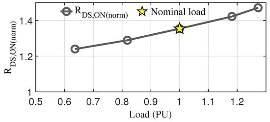
Figure 4.
GaN device on−resistance normalized to datasheet value and dynamic load per unit.
3.2. PCB-Based Inductor Parasitic Capacitance
PCB-based magnetics exhibit parasitic capacitances due to the large overlapping area and small spacing between layers. These parasitic capacitances can severely affect the converter performance. These can also resonate with inductance at higher frequencies, resulting in oscillations, and these oscillations lead to voltage and current spikes, which are responsible for EMI [30].
Given the complexity of analytical methods, determining the parasitics of the inductor is typically performed using FEA. FEA simulations revealed that the first approach as mentioned in Section 2.2 resulted in nearly double the parasitic capacitance compared to the second. Therefore, the second design approach was selected for further investigation. All the windings were placed on the top layer of the PCB to minimize the parasitic capacitances between layers. When windings are distributed across multiple layers, the proximity between the layers can create unwanted capacitances, which degrades the performance of the inductor, particularly in higher frequency designs. Keeping the windings on a single layer minimized these interlayer interactions, thereby reducing the parasitic capacitance. However, the overall impact also depends on other factors such as the PCB layout, trace spacing and the dielectric properties of the PCB material.
The parasitic capacitances in the inductor are illustrated in Figure 5a, where the turn-to-turn capacitance is represented as , the turn-to-core capacitance as and the turn-to-ground capacitance as . These three capacitances can be regarded as a parallel connected capacitor, , as shown in Figure 5b. Then, the total parasitic capacitance , as depicted in the equivalent model of the inductor, will be the sum of the individual capacitances [31].
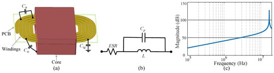
Figure 5.
PCB−based inductor: (a) different parasitic capacitances, (b) equivalent model of inductor and (c) impedance magnitude response.
The PCB inductor was initially designed in Altium and subsequently imported into Q3D to determine its parasitic capacitance. The total extracted parasitic capacitance of the inductor was found to be 3 . To validate the simulation results, the extracted parasitics including the equivalent series resistance and parasitic capacitance were modeled in LTspice. Figure 5c shows the simulated results for the impedance of the inductor. Beyond the 10 MHz range, the parasitic behavior started dominating the impedance magnitude response.
3.3. Conducted EMI
Figure 6 presents a comparison of the Fast Fourier Transform plots for the conducted emissions obtained using both SIMPLIS and FEA using the method discussed in Section 2.3. These emissions were evaluated against the CISPR 32 average measurement technique [32]. CISPR 32 defines two categories of products: Class A for industrial environments and Class B for residential environments, with Class B imposing more stringent limits than Class A. The simulation results show that some noise components exceeded the CISPR 32 Class B limit within the frequency range of 1 MHz to 5 MHz. However, the FEA simulation for the designed layout passed the Class B limit. Additionally, it was evident that the simulation results for the MHz converter from both methods closely tracked the emission trends across the frequency spectrum.
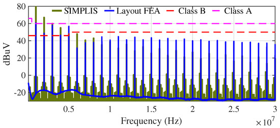
Figure 6.
Conducted EMI simulation comparison in SIMPLIS and converter PCB layout in FEA.
4. Experimental Results
This section provides details on the hardware setup used to study the operational challenges of the MHz converter. It also includes an in-depth discussion of the hardware outcomes.
4.1. Setup for Case Study of GaN Device at Beyond-Nominal Operation
The hardware test bench used to study the GaN device on-resistance behavior, losses and is shown in Figure 7. It incorporated a 900 V GaN HEMT (TP90H050WS), a SiC Schottky diode (C4D08120A) and a PCB-based inductor [2].
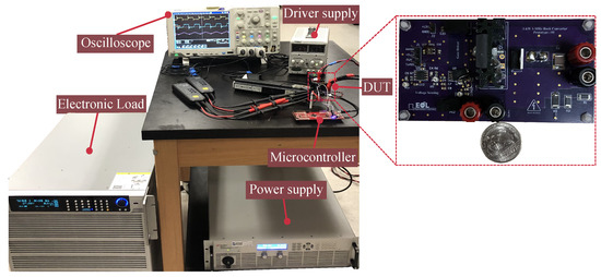
Figure 7.
Main test bench setup.
Figure 8a shows the case temperature of the GaN device under different loading conditions, as labeled. The temperature was monitored using thermocouples and a national instrument compact data acquisition unit (NI cDAQ-9174). This case temperature information was further used in the calculation of . Figure 8b illustrates the GaN device losses and the discrepancy in the error when comparing on-resistance values from the datasheet against those derived using the method mentioned in Section 2.1. It highlights a rise in the GaN device losses attributed to an increase in the on-resistance when it was subjected to beyond-nominal load conditions. It also illustrates the percent error, with losses differing by 5% at the nominal load and nearing 8% at a beyond-nominal load. Such disparities in losses can significantly accelerate the degradation of switching devices. Relying solely on datasheet values for the static on-state resistance in thermal and loss calculations can lead to inaccuracies. Device losses are closely linked to thermal management, and poor thermal management can result in shortened device lifecycles and inefficient heatsink utilization. The switching device case temperatures reached 69 °C at beyond-nominal loads, and the from the thermal network reached 85 °C, as shown in Figure 8a and Figure 8b, respectively.
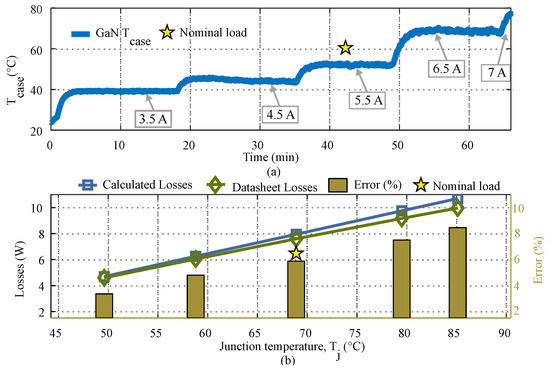
Figure 8.
(a) GaN HEMT case temperature, collected using thermocouple and national instrument compact data acquisition unit, and (b) device losses using and and error percentage for both cases.
4.2. Parasitic Capacitance in PCB-Based Inductor
Figure 9 presents an impedance sweep in LTspice incorporating the extracted parasitics and compares the results with hardware measurements. The realized inductor was characterized using an impedance analyzer (HIOKI IM3570), and the results indicated strong agreement between the impedance and phase from both the simulation and hardware up to the 5 MHz limit of the impedance analyzer. Beyond 5 MHz, resonance became evident in the simulation, and the phase shifted toward , reflecting the increasing influence of capacitive effects at frequencies beyond 5 MHz. The fabricated inductor hardware shown in Figure 10a was tested in a 1-MHz, 1-kW buck converter. Figure 10b display the waveforms of the inductor current, , and the switching node voltage, .
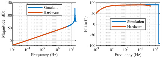
Figure 9.
Comparison of impedance and phase of PCB−based inductor with simulation and hardware.
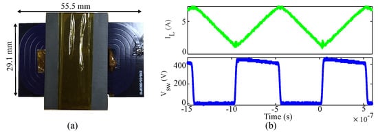
Figure 10.
(a) PCB−based inductor hardware [2] and (b) inductor current, , and converter switching node voltage, , at 1−MHz and 1−kW.
4.3. Radiated EMI
EMI tests are typically conducted in electromagnetic compliance test facilities, such as semi-anechoic chambers. However, these facilities are expensive and/or not always available in every research laboratory. As a result, alternative pre-compliance test sites, such as open-area test sites, radio frequency absorber-lined metal chambers with conductive flooring or large office and factory buildings where reflections do not interfere with measurements, can also be used [33].
The radiated EMI tests discussed in this paper were carried out at three distinct locations (, , ) following the guidelines for open-area test sites [33]. Each location was similar to the requirements in the CISPR standard when running a converter in the expected environment.
During testing, the antennae were positioned at four different orthogonal orientations (A, B, C, D) surrounding the device to capture varying emission profiles at a distance of 1 meter from the converter, as shown in Figure 11. At each location, four measurements were taken for each power level (100 W, 200 W, 300 W, 400 W). The CISPR 25 standard specifically addressing the low-frequency range of 150 kHz to 30 MHz was followed for this testing [34].
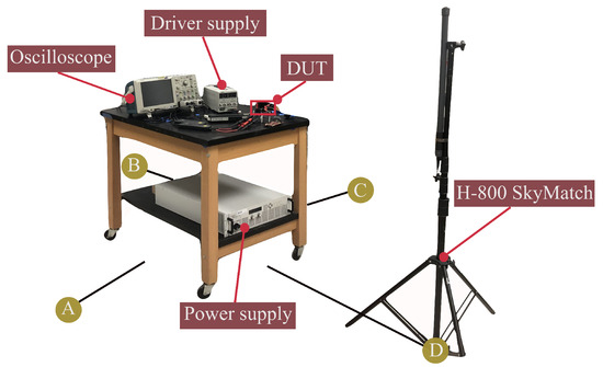
Figure 11.
Main test bench setup for radiated EMI test.
An H-800 SkyMatch antenna with a frequency range of 10 kHz to 50 MHz was used to measure the radiated emissions from the converter [35]. An R&S FSW 43 signal and spectrum analyzer operating from 2 Hz to 43.5 GHz was used for spectrum visualization [36]. To account for ambient noise, an initial measurement was conducted with all power supplies and electronic loads turned on.
Figure 12a illustrates the ambient noise levels recorded at the different locations. The remaining graphs, Figure 12b–d, were generated by averaging a set of orthogonal measurements for a single power level at each location. The radiated EMI results were compared against the CISPR 25 Class 3 and Class 5 limits. Class 3 is typically used for general automotive applications, whereas Class 5 imposes more strict limits to be employed in environments where critical communication systems, such as radars, are present. As observed, the noise levels at and generally complied with the CISPR 25 Class 5 limit, except at a few frequencies where noise exceeded the limit. In contrast, the noise levels at , particularly in the frequency range of 13 MHz to 27 MHz, appeared to exceed the limit. This could be attributed to the slightly higher ambient noise level at , as shown in Figure 12a. It may also have resulted from the location proximity to electronic devices, power lines or other radio frequency equipment. Additionally, met the Class 3 limit, while exhibited a limited noise content above this limit, specifically at 22 MHz. It is important to note that the ambient noise levels have not been subtracted from the results presented in Figure 12b–d, which may have had an impact on the frequencies which exceeded the limits of the standards.
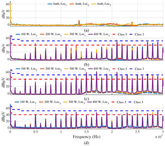
Figure 12.
Radiated EMI test results: (a) ambient noise level at different locations; (b) average waveform of four power levels at location one for four different antenna positions, (c) for location two and (d) for location three.
5. Conclusions
This paper addresses the key challenges facing MHz and kW converters by presenting a framework for future higher power density applications. It focuses on three critical areas: the dynamic on-resistance of GaN devices, parasitics in PCB-based magnetics and EMI. A simple linear model was developed to calculate changes in as a function of the losses and . The parasitic capacitance in the PCB-based inductor was investigated using FEA and validated with hardware measurements, identifying key factors, such as the PCB layers, winding thickness, PCB dielectric characteristics and interlayer spacing, which are incumbent to consider to minimize the parasitic capacitance. Radiated EMI tests revealed that the surrounding noise interference is also critical. The methodologies used in this paper are simple and adaptable to other converter topologies, providing valuable insights for the design of high-power-dense converters operating at higher switching frequencies with kilowatts of power transfer.
Author Contributions
Conceptualization, A.H. and K.B.; methodology, A.H., K.B. and D.M.; test data compiling, A.B. and R.V.; resources, K.B. and D.M.; writing, review and editing, A.H., K.B. and D.M.; supervision, K.B. and D.M.; experimental testing, A.H., K.B., A.B., R.V. and D.M. All authors have read and agreed to the published version of the manuscript.
Funding
This research received no external funding.
Data Availability Statement
The data are contained within the article. Further inquiries can be directed to the corresponding author.
Conflicts of Interest
The authors declare no conflicts of interest.
References
- Kassakian, J.G.; Jahns, T.M. Evolving and Emerging Applications of Power Electronics in Systems. IEEE J. Emerg. Sel. Top. Power Electron. 2013, 1, 47–58. [Google Scholar] [CrossRef]
- Hussain, A.; Perez, D.; Cucak, D.; Booth, K. PCB-Based Inductor Design for 1-kW, 1-MHz Buck Converter. In Proceedings of the 2024 IEEE Applied Power Electronics Conference and Exposition (APEC), Long Beach, CA, USA, 25–29 February 2024; pp. 3199–3203. [Google Scholar] [CrossRef]
- Arévalo, P.; Ochoa-Correa, D.; Villa-Ávila, E. Towards Energy Efficiency: Innovations in High-Frequency Converters for Renewable Energy Systems and Electric Vehicles. Vehicles 2025, 7, 1. [Google Scholar] [CrossRef]
- Iannaccone, G.; Sbrana, C.; Morelli, I.; Strangio, S. Power Electronics Based on Wide-Bandgap Semiconductors: Opportunities and Challenges. IEEE Access 2021, 9, 139446–139456. [Google Scholar] [CrossRef]
- Kozak, J.P.; Zhang, R.; Porter, M.; Song, Q.; Liu, J.; Wang, B.; Wang, R.; Saito, W.; Zhang, Y. Stability, Reliability, and Robustness of GaN Power Devices: A Review. IEEE Trans. Power Electron. 2023, 38, 8442–8471. [Google Scholar] [CrossRef]
- Yuan, M.; Niroula, J.; Xie, Q.; Rajput, N.S.; Fu, K.; Luo, S.; Das, S.K.; Iqbal, A.J.B.; Sikder, B.; Isamotu, M.F.; et al. Enhancement-Mode GaN Transistor Technology for Harsh Environment Operation. IEEE Electron Device Lett. 2023, 44, 1068–1071. [Google Scholar] [CrossRef]
- Qin, H.; Peng, J.; Zhang, Z.; Zhang, F.; Zhao, X.; Xu, Z. Junction temperature prediction method of GaN HEMT power devices based on accurate on-voltage testing. Energy Rep. 2023, 9, 389–395. [Google Scholar] [CrossRef]
- Yan, D.; Ma, D.B. Online Condition Monitoring for GaN Power Devices With Integrated Dynamic On-Resistance Full Profile Scan and Offset Calibration. IEEE Trans. Power Electron. 2024, 39, 6215–6224. [Google Scholar] [CrossRef]
- Li, S.; Ma, Y.; Zhang, C.; Lu, W.; Liu, M.; Li, M.; Yang, L.; Liu, S.; Wei, J.; Zhang, L.; et al. Physics-Based SPICE Modeling of Dynamic on-State Resistance of p-GaN HEMTs. IEEE Trans. Power Electron. 2023, 38, 7988–7992. [Google Scholar] [CrossRef]
- Booth, K.; Subramanyan, H.; Liang, X.; Liu, J.; Srdic, S.; Lukic, S. Optimization of Medium Frequency Transformers with Practical Considerations. In Proceedings of the 2019 IEEE Applied Power Electronics Conference and Exposition (APEC), Anaheim, CA, USA, 17–21 March 2019; pp. 2906–2911. [Google Scholar] [CrossRef]
- Nabih, A.; Jin, F.; Gadelrab, R.; Lee, F.C.; Li, Q. Characterization and Mitigation of Dimensional Effects on Core Loss in High-Power High-Frequency Converters. IEEE Trans. Power Electron. 2023, 38, 14017–14036. [Google Scholar] [CrossRef]
- Saket, M.A.; Shafiei, N.; Ordonez, M. LLC Converters With Planar Transformers: Issues and Mitigation. IEEE Trans. Power Electron. 2017, 32, 4524–4542. [Google Scholar] [CrossRef]
- Wang, S.; Pham, P.H.; Li, Q.; Nabih, A.; Prakash, P.R. PCB Winding-Based Coupled Inductor for a High-Frequency DC/DC Converter with 99% Efficiency. In Proceedings of the 2023 IEEE Applied Power Electronics Conference and Exposition (APEC), Orlando, FL, USA, 19–23 March 2023; pp. 420–425. [Google Scholar] [CrossRef]
- Chafi, A.; Idir, N.; Videt, A.; Maher, H. Design Method of PCB Inductors for High-Frequency GaN Converters. IEEE Trans. Power Electron. 2021, 36, 805–814. [Google Scholar] [CrossRef]
- Yu, Z.; Yang, X.; Wei, G.; Zhou, Y.; Xiao, Y.; Qin, M.; Wu, J.; Wang, K.; Chen, W.; Wang, L. A Novel Pyramid Winding for PCB Planar Inductors With Fewer Copper Layers and Lower AC Copper Loss. IEEE Trans. Power Electron. 2022, 37, 11461–11468. [Google Scholar] [CrossRef]
- Ma, Z.; Wang, S.; Huang, Q.; Yang, Y. A Review of Radiated EMI Research in Power Electronics Systems. IEEE J. Emerg. Sel. Top. Power Electron. 2024, 12, 675–694. [Google Scholar] [CrossRef]
- Persson, E. Optimizing PCB Layout for HV GaN Power Transistors. IEEE Power Electron. Mag. 2023, 10, 65–78. [Google Scholar] [CrossRef]
- Xu, M.; Yang, X.; Li, J. C-RC Snubber Optimization Design for Improving Switching Characteristics of SiC MOSFET. IEEE Trans. Power Electron. 2022, 37, 12005–12016. [Google Scholar] [CrossRef]
- Sun, B.; Burgos, R.; Boroyevich, D. Common-Mode EMI Unterminated Behavioral Model of Wide-Bandgap-Based Power Converters Operating at High Switching Frequency. IEEE J. Emerg. Sel. Top. Power Electron. 2019, 7, 2561–2570. [Google Scholar] [CrossRef]
- Yao, J.; Lai, Y.; Ma, Z.; Wang, S. Investigation of Noise Spectrum and Radiated EMI in High Switching Frequency Flyback Converters. In Proceedings of the 2021 IEEE Applied Power Electronics Conference and Exposition (APEC), Phoenix, AZ, USA, 14–17 June 2021; pp. 2265–2270. [Google Scholar] [CrossRef]
- Buffolo, M.; Favero, D.; Marcuzzi, A.; De Santi, C.; Meneghesso, G.; Zanoni, E.; Meneghini, M. Review and Outlook on GaN and SiC Power Devices: Industrial State-of-the-Art, Applications, and Perspectives. IEEE Trans. Electron Devices 2024, 71, 1344–1355. [Google Scholar] [CrossRef]
- Barbato, A.; Barbato, M.; Meneghini, M.; Silvestri, M.; Detzel, T.; Haeberlen, O.; Spiazzi, G.; Meneghesso, G.; Zanoni, E. Fast System to Measure the Dynamic On-resistance of On-wafer 600 V Normally Off GaN HEMTs in Hard-switching Application Conditions. IET Power Electron. 2020, 13, 2097–2103. [Google Scholar] [CrossRef]
- Yang, X.; Xu, S.; Heng, K.; Wu, X. Distributed Thermal Modeling for Power Devices and Modules With Equivalent Heat Flow Path Extraction. IEEE J. Emerg. Sel. Top. Power Electron. 2023, 11, 5863–5876. [Google Scholar] [CrossRef]
- Marek, J.; Chvála, A.; Donoval, D.; Príbytný, P.; Molnár, M.; Mikolášek, M. Compact model of power MOSFET with temperature dependent Cauer RC network for more accurate thermal simulations. Solid-State Electron. 2014, 94, 44–50. [Google Scholar] [CrossRef]
- Hussain, A.; Sado, K.; Perez, D.; Booth, K. Beyond-Nominal Operation of GaN-Based Converters for High-Power Density Applications. In Proceedings of the 2024 IEEE Transportation Electrification Conference and Expo (ITEC), Chicago, IL, USA, 19–21 June 2024; pp. 1–5. [Google Scholar] [CrossRef]
- Ferroxcube. Ferroxcube Website. Available online: https://www.ferroxcube.com/en-global (accessed on 23 September 2024).
- Yao, J.; Lai, Y.; Ma, Z.; Wang, S. Advances in Modeling and Reduction of Conducted and Radiated EMI in Non-isolated Power Converters. In Proceedings of the 2021 IEEE Applied Power Electronics Conference and Exposition (APEC), Phoenix, AZ, USA, 14–17 June 2021; pp. 2305–2312. [Google Scholar] [CrossRef]
- Ma, Z.; Lai, Y.; Yang, Y.; Huang, Q.; Wang, S. Review of Radiated EMI Modeling and Mitigation Techniques in Power Electronics Systems. In Proceedings of the 2023 IEEE Applied Power Electronics Conference and Exposition (APEC), Orlando, FL, USA, 19–23 March 2023; pp. 1776–1783. [Google Scholar] [CrossRef]
- Hussain, A.; Sado, K.; Perez, D.; Booth, K. FEA-Driven Solutions to Minimize Driving Loop Inductance and EMI in MHz PCB Designs. In Proceedings of the 2024 IEEE Sixth International Conference on DC Microgrids (ICDCM), Columbia, SC, USA, 5–8 August 2024; pp. 1–4. [Google Scholar] [CrossRef]
- Lee, S.; Kim, S.; Shin, J.; Kim, W. Analyzing and mitigating parasitic capacitances in planar transformers for high-frequency operation. J. Power Electron. 2024, 24, 946–954. [Google Scholar] [CrossRef]
- Oh, H.; Lee, J.; Lee, S.; Park, C.; Lee, J.; Lee, J.; Lee, H. Parasitic Capacitance Analysis of PCB-type Induction Heating Coil and LCCC/S Matching Network Design for Railway Turnouts. J. Electr. Eng. Technol. 2023, 18, 3311–3320. [Google Scholar] [CrossRef]
- Kharanaq, F.A.; Emadi, A.; Bilgin, B. Modeling of Conducted Emissions for EMI Analysis of Power Converters: State-of-the-Art Review. IEEE Access 2020, 8, 189313–189325. [Google Scholar] [CrossRef]
- IEEE. American National Standard for Methods of Measurement of Radio-Noise Emissions from Low-Voltage Electrical and Electronic Equipment in the Range of 9 kHz to 40 GHz; ANSI C63.4-2014 (Revision of ANSI C63.4-2009); IEEE: Piscataway, NJ, USA, 2014; pp. 1–170. [Google Scholar] [CrossRef]
- IEC. IEC Webstore. Available online: https://webstore.iec.ch/en/publication/64645 (accessed on 23 September 2024).
- H-800-SkyMatch. VLF Antennas. Available online: https://www.lfengineering.com/products.cfm#LF/VLF%20Antennas (accessed on 23 September 2024).
- R&S® FSW43. Signal and Spectrum Analyzer. Available online: https://www.rohde-schwarz.com/us/products/test-and-measurement/benchtop-analyzers/fsw-signal-and-spectrum-analyzer_63493-11793.html (accessed on 23 September 2024).
Disclaimer/Publisher’s Note: The statements, opinions and data contained in all publications are solely those of the individual author(s) and contributor(s) and not of MDPI and/or the editor(s). MDPI and/or the editor(s) disclaim responsibility for any injury to people or property resulting from any ideas, methods, instructions or products referred to in the content. |
© 2025 by the authors. Licensee MDPI, Basel, Switzerland. This article is an open access article distributed under the terms and conditions of the Creative Commons Attribution (CC BY) license (https://creativecommons.org/licenses/by/4.0/).