Abstract
This paper presents a Field-Programmable Gate Array (FPGA)-based Hardware-in-the-Loop (HIL) simulation of an Interleaved Boost Power Factor Correction (PFC) converter using the Sub-Cycle Average (SCA) modeling technique. The main objective is to achieve accurate real-time simulation performance given the hardware constraints of low-cost FPGAs. By combining the SCA modeling approach with a time-averaging correction method, the proposed model effectively reduces sampling delays and duty-cycle estimation errors arising from asynchronous Pulse Width Modulation (PWM) signal acquisition. The SCA-based converter model and time-averaging correction technique were implemented in MATLAB/Simulink R2024b using the HDL Coder environment. To validate real-time simulation accuracy, power factor improvement was evaluated for a two-phase Interleaved Boost PFC operating at a switching frequency of 60 kHz. Experimental results confirm that the proposed approach enables accurate Controller–HIL testing of power converters, even when implemented on low-cost FPGA platforms such as the Zybo Z7-10 evaluation board.
1. Introduction
Hardware-in-the-Loop (HIL) simulation techniques are widely used to efficiently verify the performance of power electronic systems and to shorten development cycles. HIL simulation converts a power electronic system into a real-time virtual model that interacts directly with actual development hardware for real-time validation [1,2]. This approach enables early verification of control algorithm stability, protection logic response, and hardware operating limits. It allows for rapid and safe system-level performance evaluation without the need for costly experimental setups or high-risk prototype testing. As shown in Figure 1, during controller development, the real-time power electronic circuit is executed on hardware such as a Central Processing Units (CPUs) or Field-Programmable Gate Arrays (FPGAs), while the controller operates by exchanging inputs and outputs under identical timing constraints.
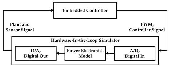
Figure 1.
Real-Time Simulation-Based Controller-HIL Configuration Diagram.
Furthermore, recent advances in power semiconductor capabilities and higher operating switching frequencies have placed greater demands on the accuracy and computational speed of HIL simulations. In particular, as energy efficiency regulations become more stringent, AC–DC and DC–DC converters including Power Factor Correction (PFC) circuits are being designed for higher efficiency and greater power capacity. Therefore, their switching frequencies have increased from several kHz to tens of kHz or higher.
Under high-frequency operating conditions, HIL simulation must periodically sample controller signals, perform real-time computations, and update the corresponding outputs. Therefore, the simulation time step () must be much smaller than the controller’s switching period (). To ensure stability and accuracy in real-time HIL simulation, is generally set to approximately 1/50–1/100 of [3,4,5]. In applications requiring high computational speed, conventional microprocessors and CPUs execute operations sequentially, making it difficult to achieve real-time processing of high-speed power electronic circuits with a time resolution below 1 µs. In contrast, FPGAs use a parallel pipeline architecture that allows multiple processing elements to operate simultaneously. This enables parallel computation of high-frequency power semiconductor models and their associated circuits with a time resolution ranging from 1 µs down to several tens of nanoseconds [6].
The PFC converter is a typical AC–DC converter that combines high-speed switching with complex operating modes. PFC is essential in improving the power factor by aligning the waveform of the AC input current with the input voltage and by reducing Total harmonic distortion (THD). In addition, PFC functionality is essential in high-efficiency power supplies and renewable energy conversion systems, where it helps suppress current distortion caused by nonlinear loads or multiphase parallel configurations. In particular, the Interleaved Boost PFC topology alternates between Continuous Conduction Mode (CCM), in which the inductor current flows continuously, and Discontinuous Conduction Mode (DCM), in which the current becomes intermittent, depending on the input voltage and operating frequency. This inductor current behavior requires an accurate current controller response and precise PWM duty computation during controller development. Accordingly, in HIL simulation, the output inductor current must deliver an accurate feedback signal to the controller with minimal delay, even under high-frequency switching conditions. Therefore, implementing this in a real-time HIL environment requires modeling techniques capable of accurately identifying the transition intervals between operating modes and precisely capturing voltage and current variations in each switching cycle.
This study applies a Sub-Cycle Average (SCA) HIL model that reduces computational complexity by averaging voltage and current variations over time in each switching cycle, combined with an average switching signal method to compensate for asynchronous sampling errors. This approach minimizes HIL simulation inaccuracies caused by mode transitions and high-frequency switching behavior in PFC converters. To validate the proposed concept in a practical hardware environment, an SCA-based interleaved Boost PFC model was implemented on the Digilent Zybo Z7-10 FPGA evaluation board, and the performance of the FPGA-based HIL simulation was verified through integration with an actual PFC controller. The AMD XC7Z010-1CLG400C device on this board was selected as the target platform because it is a widely used low-cost SoC FPGA that integrates an ARM processor and programmable logic, and its limited LUT and DSP resources provide a stringent test case for real-time implementation. By demonstrating that the SCA-based model can operate with a 200 ns simulation time step on such a resource-constrained device, the practicality of the proposed approach is confirmed for cost-sensitive industrial and educational applications.
2. Power Electronics HIL Model and Real-Time Simulation Error
2.1. Power Electronics HIL Simulation Model
Implementing power electronic circuit models is a critical step in real-time power electronics HIL simulation. To accurately reproduce the interaction between the controller and the actual power converter, the voltage and current relationships in the circuit must be accurately computed according to the simulation time step () and provided to the controller in real time. Achieving this requires the design of power electronic switch and topology models that maintain an optimal balance between accuracy and computational efficiency.
When the physical characteristics of actual power semiconductor switching devices are fully incorporated, the computational load increases exponentially, making it difficult to maintain real-time performance. Conversely, excessive simplification of these device models to reduce computational demand can distort the dynamic response of the controller. Therefore, it is crucial to establish an appropriate trade-off between physical accuracy and computational efficiency when implementing FPGA-based power electronics HIL models. Accordingly, simulation models for power semiconductor devices are generally classified into two categories: static models and transient models [7].
The transient model directly calculates the physical behavior of switching devices to reproduce detailed transient characteristics of power semiconductors, such as tail currents and reverse recovery phenomena. However, this approach requires a on the order of several nanoseconds, and its computational complexity increases considerably because the operating boundary conditions of each device must be updated at every switching event. As a result, when power electronic circuits become complex or include many switching devices, the transient model becomes inefficient for HIL implementation. Moreover, the excessive computational load can lead to FPGA resource overutilization or timing constraint violations, thereby requiring the use of high-performance FPGA hardware or additional optimization techniques for resource and timing management. Figure 2a illustrates this behavior by presenting collector-current () and collector-emitter voltage () waveforms during device turn-on and turn-off, where tail-current decay and reverse-recovery effects generate continuous nonlinear variations. This highlights the computational burden of transient modeling, as these fast dynamic intervals must be resolved at nanosecond-level timesteps to preserve switching accuracy.
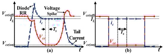
Figure 2.
Example of Comparison of transient and static switching models: (a) Transient switching waveform during turn-on/off, (b) Static model waveform during turn-on/off.
In contrast, the static model omits the detailed transient intervals of switching devices and represents only two discrete conduction states: on and off. Switching events are treated as simple state transitions, resulting in a computational structure that is simpler than that of the transient model and well suited for implementation using a fixed-step, discontinuous simulation approach. Although this simplification limits the ability to capture the detailed nonlinear behavior of power semiconductor devices, it provides sufficient accuracy for verifying control algorithms and analyzing system-level dynamic characteristics in power electronic systems. Considering the hardware constraints of low-cost FPGAs, this modeling approach enables real-time operation and efficient hardware utilization when integrated with high-speed controllers. Figure 2b shows the corresponding static switch waveform representation, where and transition directly between ON and OFF states without resolving intermediate transient slopes. This abstraction significantly reduces the required computational load and allows the HIL platform to maintain real-time execution even under switching frequencies of several tens of kHz.
2.2. Static Modeling for Real-Time Simulation
Static models used in existing commercial real-time simulators primarily include the Associated Discrete Circuit (ADC) model [8,9] and the SCA model [10,11], which is based on the average modeling approach. The ADC model performs calculations by approximating each switching element as an equivalent conductance () and current source (), as shown in Figure 3 and Table 1. The value reflects the switch’s on/off characteristics by incorporating inductive behavior during the on state and capacitive behavior during the off state. The main advantage of ADC models is their ability to reduce real-time simulation latency by preconfiguring the admittance matrix in real time according to switching events. However, as reported in [12,13], the stability of the model is highly dependent on the value of , and numerical oscillations or divergence in the simulation results may occur depending on this parameter. Furthermore, higher switching frequencies can cause the controller to become more sensitive to instantaneous current variations, potentially leading to instability in the simulation. Another limitation of this approach is that verifying controller performance under varying load conditions requires adjusting the value according to the load.
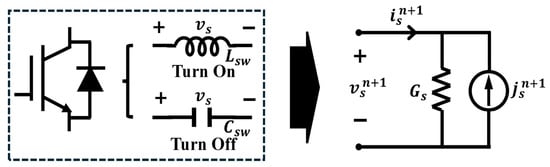
Figure 3.
Equivalent Circuit of Associated Discrete Circuit Switch Model.

Table 1.
Conductance and Current Source Values of the Associated Discrete Circuit Model.
The averaged model approximates the operation of switching devices by averaging voltage and current variations over each switching cycle. As shown in Figure 4, this approach simplifies the computational structure of power electronic circuits by replacing the instantaneous on/off transitions of switching signals with continuous averaged behavior in each cycle. However, such averaged models cannot accurately capture the current and voltage fluctuations that occur between switching transitions.
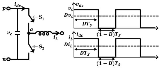
Figure 4.
Averaged Model of the Half-Bridge Switching Circuit.
Furthermore, because they are typically modeled based on the CCM operating state, additional circuit modifications and external state information are required to represent DCM operation, rectification behavior, or switching cutoff conditions.
The SCA model is an extended form of the averaged model developed to overcome its inherent limitations, as shown in Figure 5. This hybrid structure incorporates diode elements from the conventional averaged model. By averaging the switching signals on a sub-cycle basis at each , it accurately represents the instantaneous current direction and conduction path during switching events. Unlike the averaged model, the SCA model allows both CCM and DCM operations to be represented within the same framework, capturing their detailed dynamic behavior.
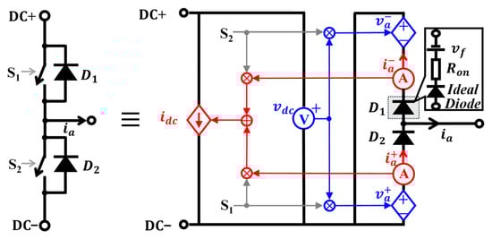
Figure 5.
Sub-Cycle Average Model of the Half-Bridge Switching Circuit.
However, this model may produce inaccuracies in the DCM operating region because the inductor current direction remains fixed in each . If the point at which the inductor current falls below zero occurs within a single , the incorrect current polarity persists throughout that period, resulting in erroneous simulation outputs [14]. In the fixed interval of a real-time simulator, when a PWM event occurs between sampling instants, the current direction cannot be updated immediately owing to sampling delays. Therefore, distortion may appear in the relationship between the output current and voltage during DCM operation. To mitigate these errors in real-time simulation particularly for high-frequency switching converters or naturally rectified converters where the current direction changes frequently it is necessary to either reduce further or apply additional techniques such as current zero-crossing detection and forced current blocking.
Furthermore, the proposed SCA-based modeling method is not limited to the interleaved Boost PFC example presented in this study. Since the switching behavior is represented on a sub-cycle basis, the same modeling approach can be applied to other converter types, including high-side and low-side choppers, half-bridge and full-bridge converters, as well as modular multi-cell topologies. This indicates that the SCA model can be easily adapted to a wide range of circuits and operating conditions with only minor modifications.
2.3. PWM Sampling Error and Compensation
As mentioned in the introduction, the HIL real-time simulator and FPGA operate with an internal sampling cycle that is faster but asynchronous to the controller’s PWM signal cycle. Therefore, when a switching event occurs in the simulation , sampling delays may appear at the boundary of the switching period [15]. As shown in Figure 6, if the PWM duty is detected with a delay by the real-time simulator or FPGA, the resulting simulation output may become inaccurate, potentially leading to improper control actions. To minimize these delays and associated simulation errors, the FPGA samples the PWM signal based on its internal clock cycle, . By operating with oversampling and performing multiple sub-cycle samples relative to the simulation model’s , simulation sampling errors can be minimized. However, setting the too short may exceed the FPGA’s computational resource capacity and violate timing constraints. Therefore, to maintain HIL simulation accuracy under hardware limitations, an additional method is required to correct errors that occur within a fixed sampling period. Signal processing or compensation techniques are necessary to offset the loss of temporal resolution caused by asynchronous sampling.
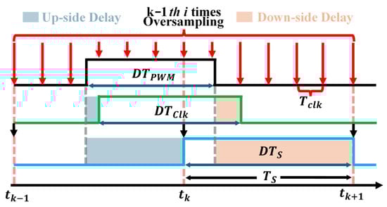
Figure 6.
Switching Signal Delay and Error as a Function of the Sampling Period.
Among the simulation correction techniques that address asynchronous sampling issues, two numerical interpolation-based methods namely the Double Interpolation Method (DIM) and the Interpolation–Extrapolation Method (IEM) have been discussed in the literature [16]. Figure 7 shows how the interpolated value at the intermediate point is estimated using the simulation results and when a PWM switching event occurs between and . If no correction algorithm is applied, the entire time step is treated as a constant ON state. In this case, the output at is calculated using the Forward Euler integration method, as expressed in (1), where denotes the state derivative evaluated under the ON-state condition and applied over the entire time step.
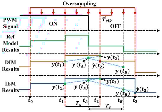
Figure 7.
Example of Double Interpolation and Interpolation–Extrapolation Algorithms.
2.3.1. Double Interpolation Method
The DIM provides more accurate signal estimates by approximating signal variations between switching events within each using a two-stage linear interpolation process. As shown in Figure 7, when a switching event occurs between two adjacent simulation instants, and , the method first calculates the intermediate value at the time instant via linear interpolation based on the simulation results and .
To determine the correction time point, the simulation result at time , advanced by one time step from , is computed. The value represents the switch-off state and is calculated using the Forward Euler integration method, as shown in (3). Here, denotes the state derivative computed under the OFF-state condition.
Based on the calculated values and , the interpolated value at time is obtained via linear interpolation, as shown in (2), and this interpolated value is subsequently computed as shown in (4).
2.3.2. Interpolation–Extrapolation Method
The IEM is similar to the DIM but omits the calculation of the intermediate estimated value . Instead, it uses the slope derived from to extrapolate the value at and predict the subsequent value , as shown in (5). Although this approach reduces computational complexity compared to DIM, accumulated interpolation errors may arise under conditions involving frequent switching events or rapid duty-cycle variations.
These interpolation-based methods inherently require additional correction computations, involving separate calculation processes for each switching state in the simulation model. Therefore, as the number of switching devices increases or the circuit topology becomes more complex, the computational burden rises exponentially. This increased computational demand can introduce simulation delays and degrade the stability of real-time execution. To address these limitations related to excessive computation and restricted real-time performance, the Time Averaging Method (TAM) [17] can be applied.
2.3.3. Time Averaging Method
The TAM is a technique used to mitigate duty-cycle errors that arise from sampling boundary mismatches. As shown in Figure 8, TAM adjusts the magnitude of the PWM switching signal in each simulation period TS in proportion to the average duty value. This is achieved by averaging the duty values of the PWM switching cycles obtained through oversampling during the clock period . The averaged switching signal , modified according to the time-averaging method from the original switching signal, can be expressed as shown in (6). Here, denotes the number of oversampled samples in the n-th simulation period , and the averaged switching signal is calculated within the range 0 ≤ ≤ 1.
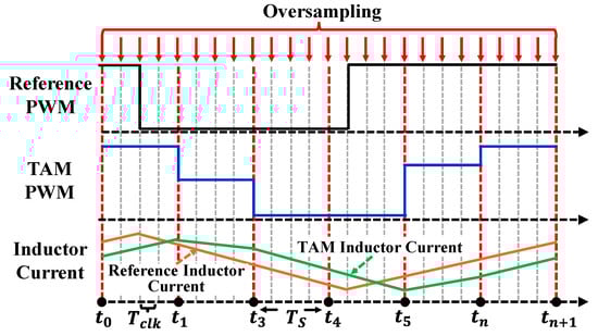
Figure 8.
Example of the Time-Average Method Correction Algorithm.
Additionally, at the end of each simulation period , the sampled switching signal is converted into its averaged value. The higher the sampling ratio between and , the greater the accuracy of the averaged switching signal . The main advantage of the time-averaging method is that it does not require complex numerical computations compared to the interpolation methods discussed earlier, thereby reducing the overall simulation computational load. When applied to SCA or averaged models, which operate by averaging switching signals over sub-cycle intervals, this method effectively minimizes control delays and duty-cycle estimation errors caused by high PWM frequencies or clock jitter.
3. Interleaved PFC Circuit and Time-Average Compensation Modeling
The Interleaved Boost PFC circuit uses a configuration in which two or more low-side chopper legs operate in an interleaved manner to achieve higher efficiency, lower current ripple, and greater power density compared to a conventional single-phase Boost PFC. Each low-side chopper is driven with a fixed phase shift, which effectively cancels input current ripple and minimizes current distortion. To implement this circuit model on the FPGA, an Interleaved Boost PFC model based on the SCA method, along with a time-averaging correction scheme for generating averaged switching signals, was developed in MATLAB/Simulink, as described in Section 2.
3.1. Sub-Cycle Average Low-Side Chopper Circuit Model
Each low-side chopper circuit was implemented as shown in Figure 9. To account for the voltage drops across the switching device and the diode, these voltage drop components were incorporated according to the switching operation. The diode conduction path is formed only when the switch is in the off state.
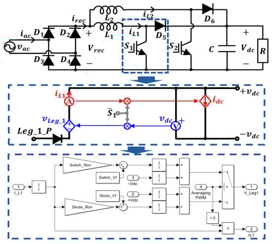
Figure 9.
Sub-Cycle Average Low-Side Chopper Model.
3.2. Zero-Current Detection and Zero-Current Blocking Inductor Current Model
As previously described, in the SCA model, reducing real-time simulation errors during DCM operation requires either decreasing or implementing a mechanism to detect when the inductor current reaches zero and block any negative current values. However, reducing may exceed the FPGA’s computational resource capacity and violate timing constraints. Therefore, the configuration shown in Figure 10 was implemented to detect and block zero-current conditions for the calculated inductor current. Additionally, the integrator used for inductor current computation was implemented using the Forward Euler method on the FPGA to achieve a simple computational structure with minimal signal delay. Further signal processing was included to reset the integrator output whenever zero-current detection occurs.
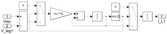
Figure 10.
Zero-Current Detection and Blocking Inductor Current Model.
3.3. Time-Averaging Method for Modeling the Averaged Switching Signal
Figure 11 shows the model used to generate the averaged switching signal. Using a multi-rate structure, the model calculates the average duty value of the actual applied PWM pulses within each simulation period , rather than relying on simple sampled PWM values, and transmits this averaged value to the low-side chopper model.
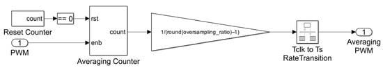
Figure 11.
Time-Averaging Correction Model for Calculating Average Switching Signals.
Figure 12 shows a simulation example of averaged switching signal generation, assuming a sampling ratio of 10. The model operates as follows: the PWM signal is connected to the enable input of the averaging counter, which increments its count by one per cycle only when the PWM signal remains in the high state. The reset counter signal resets the averaging counter to zero at the end of each , enabling the calculation of a new average duty value for the next cycle. Specifically, the counter records the total number of clock cycles during in which the PWM signal is high. The resulting value is then normalized to a duty ratio between 0 and 1 using a gain factor.
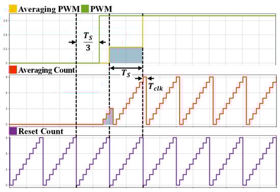
Figure 12.
Example of a Time-Averaged Calibration Model Simulation.
4. Interleaved Boost PFC FPGA Implementation and Simulation Results
The interleaved PFC circuit model was constructed by integrating the SCA low-side chopper model, the inductor model presented in Section 3, and additional components including the power source, single-phase rectifier, capacitor, and load. A DAC interface model was also incorporated to support closed-loop interaction with the external controller. The complete model was then converted into HDL code using the workflow shown in Figure 13 and subsequently deployed on the FPGA. During this process, the floating-point data format was converted into a 32Q22 fixed-point representation to satisfy the hardware resource limitations and timing constraints of the device. Based on this configuration, both the FPGA operating clock period and the PWM sampling period were set to 20 ns, while the simulation time step of the PFC model was configured to 200 ns. This allowed the 20 ns sampling interval to be achieved on a low-cost FPGA device by fully utilizing the available hardware resources. As summarized in Table 2 and Table 3, the synthesis and implementation results confirm that the proposed design meets the resource utilization and timing requirements of the XC7Z010-1CLG400C FPGA. To assess the influence of fixed-point quantization, offline simulations were carried out using the reference model, the double-precision floating-point model, and the 32Q22 fixed-point implementation, as illustrated in Figure 14. In the floating-point model, deviations from the reference model are unavoidable because asynchronous sampling effects and TAM-based time-averaging corrections are applied. When comparing the floating-point and 32Q22 fixed-point models, additional deviations occur due to quantization errors introduced by the fixed-point representation. Nevertheless, the overall dynamic behavior of the interleaved Boost PFC circuit, including switching transitions and the real-time response required for controller development and HIL verification, is accurately preserved.
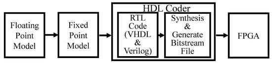
Figure 13.
Workflow Diagram for HDL Code Generation Process.
Table 2.
FPGA (XC7Z010-1CLG400C) Resource Utilization Results.
Table 3.
FPGA (XC7Z010-1CLG400C) Timing Summary Results.
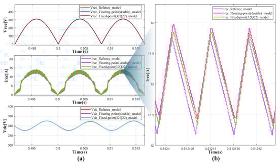
Figure 14.
Interleaved Boost PFC Off-line simulation results: (a) Reference (Matlab/Simulink Simscape), double-precision floating-point, and fixed-point models; (b) magnified view of the commutation current .
.
Figure 15 shows the hardware implementation of the Controller–HIL system, realized using the low-cost FPGA evaluation board Zybo Z7-10 (XC7Z010-1CLG400C) for the Interleaved Boost PFC. The analog feedback signal from the FPGA to the controller was generated through a Texas Instruments DAC8803EVM digital-to-analog converter. In addition, the parameters of the Interleaved Boost PFC circuit model were configured as summarized in Table 4.
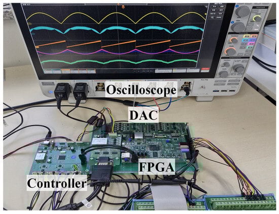
Figure 15.
Hardware Configuration for Controller–HIL Implementation.
Table 4.
Interleaved Boost PFC Circuit Parameters.
Controller–HIL Real-Time Simulation Results
The Controller–HIL simulation results for the Interleaved Boost PFC circuit are shown in Figure 16, Figure 17, Figure 18 and Figure 19. The simulation was performed under the following operating conditions: a switching frequency of 60 kHz and 100 kHz, a DC-link voltage of 380 V, and a load current ranging from 0.5 A to 8 A. Under these conditions, the rectifier current was accurately synchronized with the phase of the rectifier voltage () in accordance with PFC operation. These results confirm that the implemented PFC function effectively aligns the current waveform with the voltage waveform in phase.
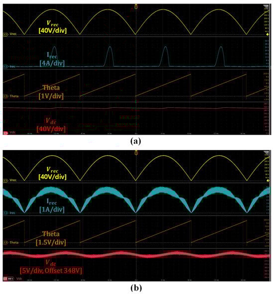
Figure 16.
Interleaved Boost PFC Real-Time Simulation Results at a Switching Frequency of 60 kHz and a Load Current of 3 A: (a) Uncontrolled PFC, (b) Controlled PFC Operation.
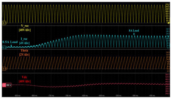
Figure 17.
Interleaved Boost PFC Real-Time Simulation Results at a Switching Frequency of 60 kHz and a Load Current Ranging from 0.5 A to 8 A.
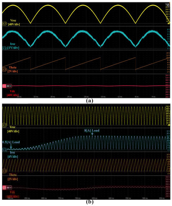
Figure 18.
Interleaved Boost PFC Real-time simulation results at a control frequency of 100 kHz: (a) load current of 3 A; (b) load current variation from 0.5 A to 8 A.
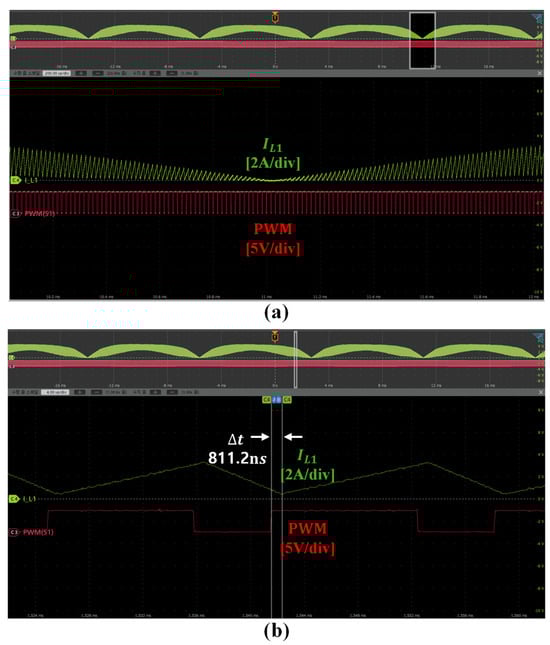
Figure 19.
Comparison of Inductor Current and PWM Signal Results: (a) DCM Operating Region, (b) Real-Time Simulation Delay Measurement Results.
Figure 19a shows the simulation results of the SCA model operating in the DCM region, which closely align with the behavior of the actual physical circuit. In practical PFC systems, the inductor current near zero can be significantly affected by noise or sensing errors, which may lead to incorrect current feedback and degraded control performance. In the proposed HIL system, however, the inductor current in the DCM region is accurately computed and supplied to the controller, ensuring stable current regulation and robust PFC operation even when the inductor current repeatedly crosses zero.
Figure 19b shows the real-time simulation delay of the inductor current when the actual PWM signal was applied. Considering both the of the PFC model and the DAC output delay, it was confirmed that the system achieved real-time operation with a total delay of <1 μs. In a practical PFC converter, a similar sub-microsecond delay is inherently introduced after the PWM command due to the propagation delay of the gate driver and the dynamic response of the power semiconductor, including the effects of parasitic elements and RC snubber networks in the switching path. Therefore, the real-time simulation delay observed in the proposed FPGA-based HIL system is consistent with the physical behavior of actual power devices and validates the realism of the implemented timing characteristics. Maintaining the total HIL-induced delay below 1 μs prevents the real-time simulator from occupying an excessive portion of the controller’s timing budget, which is especially important when validating low-cost PFC controllers with limited computational capability.
5. Discussion
Although the HIL implementation in this study was validated on a low-cost FPGA platform (Zybo Z7-10 with XC7Z010-1CLG400C), the proposed SCA-based modeling approach is essentially independent of any specific hardware device. When ported to higher-performance FPGA or FPGA–DSP architectures, the additional logic resources and timing margin can be exploited to further reduce the simulation time step, incorporate more detailed device-level switch models, or scale the method to larger converter systems. A systematic analysis of cost–performance trade-offs across different platforms remains an important direction for future research.
In addition, the synthesized design in this work includes not only the SCA low-side chopper and inductor models described in Section 3 but also the input power source, single-phase rectifier, DC-link capacitor, load model, and the DAC interface required for closed-loop operation with the physical controller. A significant portion of the LUT utilization arises from implementing the single-phase input source as a lookup-table-based sine-wave generator operating with a 200 ns simulation time step, which intentionally trades additional logic usage for deterministic timing and enables a total real-time delay of less than 1 μs. Furthermore, the HDL code was generated automatically using a model-based design flow rather than manually optimized VHDL/Verilog, which is known to be less resource-efficient and contributes to the high LUT usage reported in Table 2 (93.64%). Nevertheless, the design still meets the timing constraints and remains within the available logic, DSP, and memory resources of the XC7Z010-1CLG400C device, confirming that the proposed SCA and TAM-based HIL model is feasible even on a cost-constrained FPGA platform. Future work will explore manually optimized RTL implementations and deployment on larger FPGA or heterogeneous FPGA–DSP platforms to further reduce resource usage, support smaller simulation time steps, and extend applicability to a wider range of system-level configurations with integrated device-level switch models.
6. Conclusions
This study presented the implementation of a Controller–HIL simulation for an Interleaved Boost PFC converter based on the SCA modeling technique. By combining the SCA representation with a time-averaging (TAM) correction scheme, the proposed framework reduces real-time simulation errors caused by asynchronous sampling and CCM/DCM transitions while maintaining a fixed 200 ns simulation time step suitable for high-frequency PFC operation. The SCA-based interleaved boost PFC model was developed in a model-based design environment and implemented on a low-cost Zybo Z7-10 FPGA using a 32Q22 fixed-point format and the Forward Euler integration method, achieving Controller–HIL operation with a total closed-loop delay of less than 1 μs on the resource-constrained XC7Z010-1CLG400C device. Offline comparisons between the reference simulation model, the double-precision floating-point model, and the 32Q22 fixed-point implementation, together with the Controller–HIL measurements, showed that the key converter dynamics, including inductor current shaping and PFC behavior in both CCM and DCM regions, are accurately preserved despite quantization effects. These results indicate that the proposed SCA- and TAM-based HIL modeling approach provides a practical compromise between detailed transient modeling and conventional averaged models, enabling high-accuracy, low-latency real-time emulation of power converters on low-cost FPGA hardware. Furthermore, the framework offers a basis for extending real-time HIL implementations to a wider range of converter topologies and for integrating more detailed device-level switch models in future work.
Author Contributions
Conceptualization, T.-H.K.; methodology and software, T.-H.K. and W.-C.H.; data curation, S.-H.P. and B.-H.A.; writing—original draft preparation, T.-H.K.; writing—review and editing, T.-S.P.; supervision, T.-S.P. All authors have read and agreed to the published version of the manuscript.
Funding
This work was supported by the Korea Institute of Energy Technology Evaluation and Planning (KETEP) and the Ministry of Climate, Energy, Environment (MCEE) of the Republic of Korea (No. RS-2025-07852969). This research was supported by Basic Science Research Program through the National Research Foundation of Korea (NRF) funded by the Ministry of Education (RS-2025-25398164).
Data Availability Statement
The original contributions presented in the study are included in the article; further inquiries can be directed to the corresponding author.
Conflicts of Interest
Author Won-Cheol Hong was employed by ABOV Semiconductor Co., Ltd. Author Su-Han Pyo was employed by the Korea Electrotechnology Research Institute. Author Byeong-Hyeon An was employed by the KEPCO Research Institute. The remaining authors declare that the research was conducted in the absence of any commercial or financial relationships that could be construed as a potential conflict of interest.
References
- Mihalič, F.; Truntič, M.; Hren, A. Hardware-in-the-loop simulations: A historical overview of engineering challenges. Electronics 2022, 11, 2462. [Google Scholar] [CrossRef]
- Bullock, D.; Johnson, B.; Wells, R.B.; Kyte, M.; Li, Z. Hardware-in-the-loop simulation. Transp. Res. Part C Emerg. Technol. 2004, 12, 73–89. [Google Scholar] [CrossRef]
- Zheng, J.; Zeng, Y.; Zhao, Z.; Liu, W.; Xu, H.; Ji, S. A semi-implicit parallel leapfrog solver with half-step sampling technique for FPGA-based real-time HIL simulation of power converters. IEEE Trans. Ind. Electron. 2023, 71, 2454–2464. [Google Scholar] [CrossRef]
- Liu, J.; Xu, M.; Yang, H.; Que, Z.; Gu, W.; Tang, Y.; Wang, B.; Li, H. FPGA Accelerated Large-Scale State-Space Equations for Multi-Converter Systems. Electronics 2025, 14, 3966. [Google Scholar] [CrossRef]
- Xu, H.; Zheng, J.; Zeng, Y.; Liu, W.; Zhao, F.; Qu, C.; Zhao, Z. Topology-aware matrix partitioning method for FPGA real-time simulation of power electronics systems. IEEE Trans. Ind. Electron. 2023, 71, 7158–7168. [Google Scholar] [CrossRef]
- Blanchette, H.F.; Ould-Bachir, T.; David, J.P. A state-space modeling approach for the FPGA-based real-time simulation of high switching frequency power converters. IEEE Trans. Ind. Electron. 2011, 59, 4555–4567. [Google Scholar]
- Bai, H.; Liu, C.; Majstorovic, D.; Gao, F. Real-Time Simulation Technology for Modern Power Electronics; Elsevier: Amsterdam, The Netherlands, 2023. [Google Scholar]
- Hui, S.; Christopoulos, C. A discrete approach to the modelling of power electronic switching networks. In Proceedings of the 20th Annual IEEE Power Electronics Specialists Conference, Blackpool Winter Gardens, UK, 26–29 June 1989. [Google Scholar]
- Dufour, C.; Cense, S.; Ould-Bachir, T.; Gregoire, L.-A.; Belanger, J. General-purpose reconfigurable low-latency electric circuit and motor drive solver on FPGA. In Proceedings of the IECON 2012-38th Annual Conference on IEEE Industrial Electronics Society, IEEE, Montreal, QC, Canada, 25–28 October 2012. [Google Scholar]
- Allmeling, J.; Felderer, N. Sub-cycle average models with integrated diodes for real-time simulation of power converters. In Proceedings of the 2017 IEEE Southern Power Electronics Conference (SPEC), IEEE, Puerto Varas, Chile, 4–7 December 2017. [Google Scholar]
- Osório, C.R.; Genic, A.; Costa, S. Introduction to Typhoon HIL: Technology, functionalities, and applications. In Real-Time Simulation and Hardware-in-the-Loop Testing Using Typhoon HIL; Springer: Singapore, 2023; pp. 1–28. [Google Scholar]
- Guo, X.; Tang, Y.; Wu, M.; Zhang, Z.; Yuan, J. FPGA-based hardware-in-the-loop real-time simulation implementation for high-speed train electrical traction system. IET Electr. Power Appl. 2020, 14, 850–858. [Google Scholar] [CrossRef]
- Alsarayreh, S.; Sütő, Z. Optimal Selection of Switch Model Parameters for ADC-Based Power Converters. Energies 2023, 17, 56. [Google Scholar] [CrossRef]
- Allmeling, J. Controller-HIL Testing for GaN and SiC Converters. EE Power. 2024. Available online: https://eepower.com/technical-articles/controller-hil-testing-for-gan-and-sic-converters/ (accessed on 24 October 2025).
- Matar, M.; Karimi, H.; Etemadi, A.; Iravani, R. A high performance real-time simulator for controllers hardware-in-the-loop testing. Energies 2012, 5, 1713–1733. [Google Scholar] [CrossRef]
- Li, F.; Wang, Y.; Wu, F.; Huang, Y.; Liu, Y.; Zhang, X.; Ma, M. Review of real-time simulation of power electronics. J. Mod. Power Syst. Clean Energy 2020, 8, 796–808. [Google Scholar] [CrossRef]
- Lian, K.; Lehn, P. Real-time simulation of voltage source converters based on time average method. IEEE Trans. Power Syst. 2005, 20, 110–118. [Google Scholar] [CrossRef]


Disclaimer/Publisher’s Note: The statements, opinions and data contained in all publications are solely those of the individual author(s) and contributor(s) and not of MDPI and/or the editor(s). MDPI and/or the editor(s) disclaim responsibility for any injury to people or property resulting from any ideas, methods, instructions or products referred to in the content. |
© 2025 by the authors. Licensee MDPI, Basel, Switzerland. This article is an open access article distributed under the terms and conditions of the Creative Commons Attribution (CC BY) license (https://creativecommons.org/licenses/by/4.0/).