Abstract
Hybrid solar cells, which combine inorganic and organic materials, offer a promising pathway to achieve low cost, flexible, high-performance photovoltaic devices. This work explores the application of oxidative chemical vapor deposition (oCVD) to deposit poly(3,4-ethylenedioxythiophene) (PEDOT) as a transparent hole transfer layer in hybrid solar cells. Unlike solution-processed PEDOT with polystyrene sulfonate solubilizer (PEDOT:PSS), oCVD allows for growing high-purity PEDOT that provides conformal coverage on textured substrates, enabling enhanced antireflective effects and improved charge extraction. We discuss the advantages of oCVD PEDOT in hybrid architecture, its compatibility with textured substrates, and its potential to achieve higher efficiency.
1. Introduction
Hybrid solar cells (HSCs) represent a promising avenue for sustainable energy generation by combining the advantages of organic and inorganic materials. These devices aim to combine the high efficiency and stability of inorganic semiconductors (such as silicon) with the low-cost, ease of processing, and tunable optoelectronic properties of organic electronic materials. As the global demand for renewable energy grows, HSCs offer a promising alternative to conventional silicon-based solar cells, particularly for applications requiring flexibility, lightweight design, and cost-effective manufacturing [1]. Among these, PEDOT:PSS (poly(3,4-ethylenedioxythiophene)-polystyrene sulfonate)-based hybrid solar cells have gained significant attention due to the maturity of their technology and the demonstrated potential for high-performance heterojunction photovoltaic devices [2].
PEDOT:PSS is a well-studied conductive polymer known for its high transparency, high conductivity, and compatibility with solution-based processing techniques (e.g., spin coating). When paired with silicon (Si), PEDOT:PSS forms a heterojunction that facilitates efficient charge separation and transport. The PEDOT:PSS/Si HSCs combine the high carrier mobility of silicon and the flexibility of PEDOT:PSS, enabling the fabrication of lightweight, flexible, and potentially low-cost solar cells. However, the PSS component, which induces the water solubility of the polymer, is insulating and can hinder charge transport if not properly phase-separated from PEDOT [3]. Recent work shows that PEDOT films without the PSS solubilizer exhibit extraordinary conductivities (>7500 S/cm) [4], which are much higher than PEDOT:PSS films optimized with co-solvents (1000 S/cm) [5] such as dimethyl sulfoxide (DMSO) or ethylene glycol (EG) [4,5]. In addition to inferior conductivity, PEDOT:PSS films suffer from challenges posed by solution-based processing, such as poor conformality to non-planar surfaces due to surface tension effects and poor uniformity of film thickness, etc. [6]. PEDOT:PSS films can suffer from pinholes or cracks because of their inhomogeneous film morphology, leading to shunting paths and reduced fill factor (FF), especially with textured Si wafers [7,8].
Oxidative chemical vapor deposition (oCVD) is a vapor-phase polymerization technique that enables the synthesis and deposition of conductive polymers, such as PEDOT, in a single step without the use of a solvent medium or a solubilizer [9]. Unlike conventional solution-based methods like spin coating, oCVD utilizes vaporized monomers (e.g., EDOT) and oxidants (e.g., vanadium oxytrichloride [VOCl3] and antimony pentachloride [SbCl5]) that react on a substrate under low-pressure conditions to form the conjugated PEDOT polymer film directly on the substrate surface [10] (see Figure 1). This process allows for precise control over film thickness and morphology, which makes it suitable for applications that need uniform and conformal coatings on non-planar topologies [11]. This is one of the key strengths of depositing PEDOT films with the oCVD process, which is also a critical requirement for advanced optoelectronic devices such as solar cells. The conformality and uniformity of the PEDOT film is essential for optimizing the anti-reflective effect in these hybrid photovoltaic architectures that is needed to maximize the light absorption of the devices [7].
In addition to superior film growth control, oCVD PEDOT can exhibit excellent electrical conductivity by eliminating the insulating PSS component that is needed for solution-based processing. The mild heating requirement (~100 °C) makes oCVD compatible with temperature-sensitive substrates. Furthermore, oCVD PEDOT, as a hole transfer layer in an inverted perovskite solar cell, has shown to yield a higher power conversion efficiency compared to conventional PEDOT:PSS-based counterparts due to higher film quality with the greater in-plane π-π stacking and shorter stacking distance that enhances charge transport [12,13]. These advantages make oCVD a versatile and scalable method for integrating PEDOT into next-generation devices, including hybrid solar cells, where it can serve as a hole transport layer and an effective antireflective coating. By decoupling optical and electrical pathways through homogeneous coatings, oCVD PEDOT enables innovative device designs that push the limits of efficiency and functionality in thin-film photovoltaics [14]. Although oCVD PEDOT, as mentioned above, has been used in some photovoltaic applications, such as perovskite solar cells, relevant work in the field of conformable, hybrid thin-film solar cells is still lacking. In this work, we employed oCVD-deposited PEDOT as the hole transport layer in hybrid solar cells, achieving uniform coverage on a textured silicon wafer with decent conversion efficiencies.

Figure 1.
oCVD of PEDOT. (a) oCVD reactor setup, showing vapor flow of monomers and oxidants into a vacuum chamber, where the monomer EDOT polymerizes into a thin-film PEDOT polymer on a substrate. (b) oCVD step-growth reaction mechanism [15], illustrating the oxidation by the oxidant of the EDOT monomer into cation radicals, which then undergo oxidative polymerization to produce the oxidized, conductive form of the PEDOT polymer.

2. Materials and Methods
Si wafer preparation: N-type (100)-oriented silicon substrates (phosphorus-doped) with a back surface field (BSF) were prepared, with a thickness of 145 μm and a bulk resistivity of 1–5 Ω-cm. Both sides of the wafers were randomly etched in 2% potassium hydroxide (KOH), producing textured pyramid structures with base sizes of 3–5 μm. The BSF n+ layer was formed through phosphorus oxychloride (POCl3) diffusion at 820°C for 15 min under a carrier gas flow rate of 1500 sccm, enabling phosphosilicate glass (PSG) growth and dopant drive-in, followed by a 10 min buffered oxide etch to remove the PSG, resulting in a sheet resistance of 55 Ω/□. Prior to oCVD deposition, the wafers were cleaned via a five-minute Piranha etch (H2SO4:H2O2 = 4:1 v/v), a five-minute deionized water rinse, and a two-minute immersion in 2 wt% hydrofluoric acid (HF) [16]. The substrates were then dried under nitrogen flow and loaded into the oCVD reaction chamber, where varying deposition conditions were applied across the samples.
oCVD process: In the oCVD process, precisely controlled flows of monomer and oxidant vapors are introduced into a temperature-regulated vacuum chamber via a calibrated mass flow system. When the monomer vapors interact with the oxidant, they initiate step-growth polymerization, resulting in the formation of a π-conjugated PEDOT thin-film [14]. This process simultaneously facilitates in situ doping through the incorporation of chloride ions (Cl−) as counterion dopants. Following polymerization, volatile byproducts of the oxidant desorb from the film surface and are evacuated from the reaction chamber.
The oCVD reactor setup and the poly(3,4-ethylenedioxythiophene) (PEDOT) polymerization chemistry are shown in Figure 1. The monomer, 3,4-ethylenedioxythiophene (EDOT; 97% AstaTech, Bristol, PA, USA), and the oxidants, vanadium oxytrichloride (VOCl3; 99% Millipore Sigma, Burlington, MA, USA) and antimony pentachloride (SbCl5; 99% MilliporeSigma, Burlington, MA, USA), were used without further purification. The polymer, PEDOT, was deposited onto 1.5 cm × 1.5 cm patterned silicon substrates placed inside a 30 × 25 × 5 cm3 custom-built stainless steel vacuum chamber with a metal lid. Prior to deposition, the reactor was pumped down to base pressure using a rotary vane vacuum pump (Edwards Vacuum, Burgess Hill, UK). The monomer and oxidant vapors were individually metered into the reactor chamber using precision stainless steel needle valves (Swagelok, Solon, OH, USA) at 2 sccm each. To achieve sufficient vapor flow rates, the monomer source vessel was heated to 125 °C, and the oxidant source vessel was gently heated to 30 °C as it has relatively high vapor pressure. To facilitate the transport of the precursor species into the reactor, inert nitrogen gas was metered through each line at 1 sccm using a mass flow controller (MKS Instruments, Andover, MA, USA). The monomer was fed from one side of the reactor, and the oxidant was fed through a nozzle that is perpendicular to the direction of the monomer flow. The substrates were placed near the oxidant nozzle where PEDOT deposition takes place. A variation in device performance was observed as a function of the placement of the substrate relative to the oxidant nozzle. The stage was heated to achieve a substrate temperature ranging from 95 to 140 °C, which is chosen to be slightly greater than the glass transition temperature (Tg) of PEDOT [17]. The rest of the reactor was kept 15 °C hotter than the substrate to suppress deposition outside of the substrate area. The reactor pressure was automatically maintained at 1 Torr with a pressure controller (MKS Instruments, Andover, MA, USA) in a feedback loop with a pressure gauge (MKS Instruments, Andover, MA, USA) and a downstream throttle valve (MKS Instruments, Andover MA). Each deposition was carried out for a duration ranging from 5 to 80 min, after which the precursor flows were stopped, and the reactor heating was shut off to allow the reactor to return to base pressure and near room temperature. The reactor was then vented to the atmosphere to retrieve the PEDOT-coated samples.
Post-treatment and J-V measurements: For the fabrication of the complete solar cell devices, metal contacts were deposited via electron beam-physical vapor deposition (EBPVD). A 2 µm-thick aluminum layer was evaporated onto the back side (BSF-treated surface) to form the rear contact, while a 500 nm-thick silver front contact was also evaporated using a previously optimized finger-bus bar shadow mask directly on the top of the PEDOT layer (shown in Figure 2) [2].
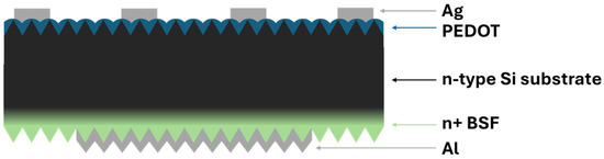
Figure 2.
Schematic of hybrid PV device architecture. Dark green represents PEDOT, black is Si substrate, and light green represents n+ Back Surface Field.
The devices were fabricated on textured n-type silicon substrates with the size of 1.5 cm × 1.5 cm. Current density–voltage (J–V) characteristics were evaluated under dark and illuminated conditions using a Keithley 2400 Sourcemeter (Tektronix, Solon, OH, USA). Light J–V measurements were performed under standard air mass AM 1.5G solar irradiation (100 mW/cm2) [2].
3. Results and Discussion
3.1. Experiment Conditions and J-V Test Results
The superior properties of oCVD PEDOT (higher free-carrier concentration and mobility compared to solution-processed PEDOT:PSS) that give it the potential to yield higher-performance hybrid PV devices critically depend on the optimization of reaction conditions. Key parameters include the following: (1) the selection of oxidant-doping molecules, (2) reaction kinetics (governed by reactor temperature and pressure), and (3) deposition time. These factors must be carefully controlled to achieve optimal conductivity, conformal coverage on the textured silicon substrate, and uniform, pinhole-free films.
Table 1 below outlines the reaction conditions tested and the best recorded device efficiency among all the fabricated devices (usually eight).

Table 1.
oCVD reaction conditions and device results.
In oCVD, the polymerization of the precursors directly on the substrate surface is a critical step that influences film uniformity, growth rate, and resulting film properties. Several factors affect precursor adsorption, including substrate temperature, precursor vapor pressure, and chamber pressure. The results shown above in Table 1 demonstrate the impact of these factors on PEDOT film quality and the resulting performance of the PV devices.
One of the crucial factors that influence the oCVD process is the substrate temperature. There is competition between precursor adsorption and intrinsic polymerization reaction kinetics with increasing substrate temperature that impacts film growth, overall deposition rate, and resulting film thickness. Lower temperatures promote stronger vapor adsorption but reduce polymerization kinetics, while higher temperatures accelerate the reaction kinetics but greatly reduce precursor adsorption to the substrate. In general, lower deposition rates typically yield higher film quality and more conformal thin films, while higher deposition rates often mean reduced film quality and greater difficulty in controlling the film thickness and film conformality [17]. As shown in Table 1, the temperatures used in this work are in the range of 95–140 °C, and the higher power conversion efficiencies were generally obtained with substrate temperatures higher than 100 °C, which is higher than the glass transition temperature of PEDOT (64–100 °C) [17,18] and result in films with superior conductivity, as discussed by Heydari et al. [19]. Furthermore, as can be seen in Table 1, there is an optimal reaction temperature in this apparatus at 125 °C when using VOCl3 as the oxidant, which yields the highest device efficiency. This is attributed to a balance between better PEDOT film quality in terms of conformality and crystallinity while maintaining a modestly high deposition rate at an intermediate temperature. This temperature regime offers multiple advantages, including cost reduction in processing, enhanced compatibility with thermally sensitive substrates, and minimizing hazardous chemical usage. These conditions also maximize the benefits of using a liquid oxidant instead of solid oxidant such as FeCl3, which would require an acidic rinsing step to remove the residual oxidant [17].
Precursor vapor pressure and reactivity are equally important. High-vapor–pressure oxidants enable slower adsorption but require more careful heating during the reaction stage for optimal delivery and resulting film homogeneity. VOCl3 was chosen as the oxidant molecule over SbCl5 because it was expected to result in a more homogeneous coating on textured substrates due to a lower sticking coefficient resulting from its lower molecular weight and higher vapor pressure, while providing a similar degree of oxidative doping [20]. As shown in Table 1, when using SbCl5 as the oxidant, the device efficiency was much lower compared to when using VOCl3. Due to the lower vapor pressure of SbCl5, the deposition time and reactor pressures had to be adjusted to reduce the deposition rate and enhance deposition control. However, maintaining precise PEDOT film thicknesses was very challenging with SbCl5 since it is highly reactive with PEDOT. Despite our best efforts, the resulting device performance was poorer under all conditions tested.
Due to the limitation of flow rate of the oxidant and monomer, as well as the difficulty of controlling the reaction stage temperature evenly, the growth rate of PEDOT was affected by the placement of the substrate relative to the oxidant inlet nozzle, and, as a result, greatly affected the device performance. As shown in Figure 3 and Table 2, the sample that was placed remote from the oxidant nozzle presented lower open circuit voltage (Voc), short circuit current (Jsc), and fill factor compared with the one near the nozzle, which led to conversion efficiencies of 8.5% and 4.7%, respectively. Although the performances of the samples located farther from the nozzle exhibited different performance compared to the others, those placed close to the oxidant nozzle showed similar results. For example, the three closest samples to the oxidant nozzle exhibited a low standard deviation of 8.4 ± 0.1% with reaction conditions of 1000 mTorr, 125 °C, and 80 min. This indicates overall experimental stability.
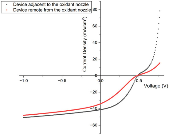
Figure 3.
J-V test results in light for devices placed adjacent to (black) and remote from (red) the oxidant nozzle.
Table 2.
Solar cell JV metrics for devices placed adjacent to (device 1) and remote from (device 2) the oxidant nozzle.
3.2. Surface Morphology and Thickness
Random pyramid KOH-textured silicon substrates are preferred for solar cell fabrication over planar substrates (particularly silicon heterojunction designs) due to their superior light-trapping and anti-reflection properties, which reduce surface reflection from over 35% to ~10% without requiring additional antireflective coatings [21,22]. The microscale pyramids enhance photon absorption by scattering light and increasing the effective optical path length, while their larger surface area improves charge carrier collection near the emitter. However, although the textured silicon substrate significantly improves the performance of the solar cells by improving the light-trapping ability of the device, it causes challenges in the conformal deposition of subsequent layers compared to planar substrates. Conventional solution-based deposition methods like spin coating face significant challenges to achieve uniform film coverage on these textured surfaces because of the presence of surface tension effects, which leads to thickness variations at different positions of the wafer that increase series resistance and parasitic optical losses. The oCVD processes on the other hand, overcomes the non-uniformity challenges and the formation of pinholes during deposition due to the absence of liquid solvent interactions with the silicon substrate [8,19].
Cross-sectional SEM images revealed significant non-uniformity in PEDOT: PSS films deposited via spin coating on textured pyramid structures (Figure 4a,b). The thickness variation was particularly striking, with valley regions accumulating excessively thick coatings (up to 369 nm) while peak areas showed inconsistent coverage ranging from 44 nm to 100 nm. This extreme thickness variation affects not only current extraction in the solar cell but also contributes to parasitic light absorption losses. The interfacial conformity issues at both PEDOT: PSS/Si and Ag/PEDOT: PSS interfaces also directly contribute to elevated series resistance. In contrast, oCVD-processed films overcome these spin-coating limitations. As shown in Figure 4c,d, PEDOT layers deposited by the oCVD technique can achieve conformal deposition regardless of substrate topography, achieving uniform thickness across peaks and valleys. It is obvious that there is no excess material accumulation in recessed regions, which always occurs during solution-based processing methods.
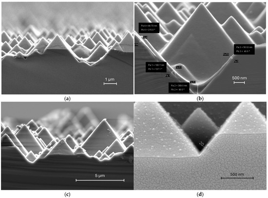
Figure 4.
SEM of textured wafers with (a,b) PEDOT: PSS deposited by spin coating [23] at low and high magnification, respectively and (c,d) PEDOT deposited by oCVD at low and high magnification respectively.
In addition to uniformity, oCVD technology provides more precise thickness control compared to solution-based deposition methods. As a vapor-phase process, oCVD enables atomic-level precision through the controlled reaction of gaseous monomers and oxidants on the substrate surface, with the thickness determined by precisely controlled parameters like reaction temperature, time, and precursor flow rates. Since there is no solvent during deposition, effects that could distort films, such as drying-induced shrinkage or coffee-ring effects, will not occur. In contrast, solvent-based processes suffer from the inherent variability caused by fluid dynamics, solvent evaporation, and centrifugal forces. As a result, a thinner PEDOT layer (~20 nm as shown in Figure 4d) can be achieved with oCVD, which is difficult to accomplish with the commonly used spin-coating method on textured Si wafers because of the risk of incomplete coverage and pinhole formation. This precise thickness control can achieve a uniform PEDOT layer with an optimized thickness that falls into the range of the diffusion length of the conjugated polymer, which significantly reduces the losses caused by parasitic light absorption, carrier recombination, and contributes to series resistance [24]. Furthermore, since the oCVD technique is a vacuum-based process, it offers superior reproducibility compared to spin coating that is sensitive to environmental conditions and operator skills, making it far more suitable for the industrial-scale production of high-performance photovoltaic devices.
For a comprehensive evaluation, the performance of solar cells fabricated with oCVD PEDOT was compared to a device fabricated with traditional spin-coated PEDOT:PSS. It is important to note that there is a two-hour interval between the HF clean step and the oCVD deposition step, imposed by instrumental and experimental limitations, which inevitably led to the regrowth of native SiO2 on the silicon wafers. This factor is known to significantly impact device performance. For a proper comparison, experiments our group conducted previously, where silicon wafers were exposed in an ambient atmosphere for varying durations after HF-cleaning and before spin coating are referenced [23]. As shown in Table 3, tdonehe device with a two-hour delay yielded an efficiency of 4.8%, with its Voc, Isc, and fill-factor FF all lower than the values achieved by our best oCVD solar cell with an efficiency of 8.5%. This direct comparison under the same oxide regrowth condition demonstrates the advantage of the oCVD technique, showing that oCVD-deposited PEDOT can effectively enhance the performance of solar devices likely by enhancing the conductivity of the PEDOT layer, enabling superior conformal coverage and facilitating more efficient charge transport across the interface [12].
Table 3.
Solar cell JV metrics for devices fabricated with spin-coated PEDOT:PSS with 2 h exposure in ambient air.
4. Summary
In this work, oCVD processing was used for the fabrication of hybrid solar cells. Conjugated PEDOT films were deposited on a textured silicon substrate under solvent-free conditions. Although further exploration of experimental conditions is still needed to obtain optimal performance, a device with decent performance is demonstrated (Voc 0.484V, Jsc 41.3 mA/cm2, FF 42.4, power efficiency 8.5%) which indicates that there is potential for the oCVD deposition of PEDOT to be a competitive processing technique for the fabrication of high-performance HSCs. During our work, it was noted that the homemade oCVD tool presented challenges related to substrate temperature control and placement relative to the reactant inlet. A real-time monitoring system, such as spectroscopic ellipsometry or quartz crystal microbalance, would be useful in monitoring in situ deposition conditions. Another existing issue is the residual oxidant, especially at higher temperatures. To achieve a higher reaction rate, an acidic rinsing step is needed to remove the residual oxidant. Furthermore, to further improve the performance of the device, apart from the optimization the oCVD process, a proper compatible silicon surface passivation step would be required to minimize the recombination losses at the organic–inorganic interface.
Author Contributions
Conceptualization, D.A.T., R.L.O. and K.K.S.L.; Methodology K.K.S.L.; Validation, G.L., D.A.T. and V.S.P.; Investigation, G. Li, D.A.T. and V.S.P.; Writing—Original Draft Preparation, G.L.; Writing—Review and Editing, D.A.T., V.S.P., R.L.O. and K.K.S.L.; Visualization, V.S.P. and G.L.; Supervision, Project Administration, and Funding Acquisition, R.L.O. and K.K.S.L. All authors have read and agreed to the published version of the manuscript.
Funding
This research was funded by the National Science Foundation, grant number 2141122, PFI-TT: next-generation hybrid solar cells enabling lower cost, safe, and environmentally friendly floating photovoltaic installations.
Data Availability Statement
The datasets used and analyzed in this study are available from the corresponding author upon reasonable request.
Acknowledgments
During the preparation of this manuscript, the author used DeepSeek-V2 for the purpose of language editing in the first draft. The authors have reviewed and edited the output and take full responsibility for the content of this publication.
Conflicts of Interest
The authors declare no conflicts of interest.
Abbreviations
The following abbreviations are used in this manuscript:
| oCVD | Oxidative chemical vapor deposition |
| PEDOT | Poly(3,4-ethylenedioxythiophene) |
| PEDOT:PSS | Poly(3,4-ethylenedioxythiophene)-polystyrene sulfonate |
| EDOT | 3,4-ethylenedioxythiophene |
| FF | Fill factor |
References
- Günes, S.; Sariciftci, N.S. Hybrid solar cells. Inorg. Chim. Acta 2008, 361, 581–588. [Google Scholar] [CrossRef]
- Iyer, A.; Hack, J.; Angel Trujillo, D.A.; Tew, B.; Zide, J.; Opila, R. Effects of Co-Solvents on the Performance of PEDOT:PSS Films and Hybrid Photovoltaic Devices. Appl. Sci. 2018, 8, 2052. [Google Scholar] [CrossRef]
- Sun, Z.; He, Y.; Xiong, B.; Chen, S.; Li, M.; Zhou, Y.; Zheng, Y.; Sun, K.; Yang, C. Performance-Enhancing Approaches for PEDOT:PSS-Si Hybrid Solar Cells. Angew. Chem. Int. Ed. 2021, 60, 5036–5055. [Google Scholar] [CrossRef] [PubMed]
- Heydari Gharahcheshmeh, M.; Robinson, M.T.; Gleason, E.F.; Gleason, K.K. Optimizing the Optoelectronic Properties of Face-On Oriented Poly(3,4-Ethylenedioxythiophene) via Water-Assisted Oxidative Chemical Vapor Deposition. Adv. Funct. Mater. 2021, 31, 2008712. [Google Scholar] [CrossRef]
- Shi, H.; Liu, C.; Jiang, Q.; Xu, J. Effective approaches to improve the electrical conductivity of PEDOT: PSS: A review. Adv. Electron. Mater. 2015, 1, 1500017. [Google Scholar] [CrossRef]
- Xing, R.; Wang, S.; Zhang, B.; Yu, X.; Ding, J.; Wang, L.; Han, Y. Inkjet printed polystyrene sulfuric acid-doped poly (3, 4-ethylenedioxythiophene) (PEDOT) uniform thickness films in confined grooves through decreasing the surface tension of PEDOT inks. RSC Adv. 2017, 7, 7725–7733. [Google Scholar] [CrossRef]
- Xia, Z.; Gao, P.; Sun, T.; Wu, H.; Tan, Y.; Song, T.; Lee, S.-T.; Sun, B. Buried MoO x/Ag Electrode Enables High-Efficiency Organic/Silicon Heterojunction Solar Cells with a High Fill Factor. ACS Appl. Mater. Interfaces 2018, 10, 13767–13773. [Google Scholar] [CrossRef] [PubMed]
- Heydari Gharahcheshmeh, M.; Gleason, K.K. Device fabrication based on oxidative chemical vapor deposition (oCVD) synthesis of conducting polymers and related conjugated organic materials. Adv. Mater. Interfaces 2019, 6, 1801564. [Google Scholar] [CrossRef]
- Gleason, K.K. CVD Polymers: Fabrication of Organic Surfaces and Devices; John Wiley & Sons: Hoboken, NJ, USA, 2015. [Google Scholar]
- Lahann, J.; Klee, D.; Pluester, W.; Hoecker, H. Bioactive immobilization of r-hirudin on CVD-coated metallic implant devices. Biomaterials 2001, 22, 817–826. [Google Scholar] [CrossRef] [PubMed]
- Nejati, S.; Minford, T.E.; Smolin, Y.Y.; Lau, K.K.S. Enhanced charge storage of ultrathin polythiophene films within porous nanostructures. ACS Nano 2014, 8, 5413–5422. [Google Scholar] [CrossRef] [PubMed]
- Chowdhury, K.; Behura, S.K.; Rahimi, M.; Heydari Gharahcheshmeh, M. oCVD PEDOT-Cl Thin Film Fabricated by SbCl5 Oxidant as the Hole Transport Layer to Enhance the Perovskite Solar Cell Device Stability. ACS Appl. Energy Mater. 2024, 7, 1068–1079. [Google Scholar] [CrossRef]
- Aksimentyeva, O.I.; Horbenko, Y.Y.; Savchyn, V.P.; Demchenko, P.Y.; Popov, A.I. Micro- and Nanocomposites of Barium Zirconate Incorporated in Polymer Matrix. In Proceedings of the Nanomaterials and Nanocomposites, Nanostructures, and Their Applications, Bukovel, Ukraine, 16–19 August 2023; Springer: Cham, Switzerland, 2024; pp. 1–12. [Google Scholar]
- Barr, M.C.; Rowehl, J.A.; Lunt, R.R.; Xu, J.; Wang, A.; Boyce, C.M.; Im, S.G.; Bulović, V.; Gleason, K.K. Direct monolithic integration of organic photovoltaic circuits on unmodified paper. Adv. Mater. 2011, 23, 3500. [Google Scholar] [CrossRef] [PubMed]
- Lock, J.P.; Im, S.G.; Gleason, K.K. Oxidative Chemical Vapor Deposition of Electrically Conducting Poly(3,4-ethylenedioxythiophene) Films. Macromolecules 2006, 39, 5326–5329. [Google Scholar] [CrossRef]
- Chen, M.; Hack, J.; Iyer, A.; Lin, X.; Opila, R.L. Chemical and Electrical Passivation of Semiconductor Surfaces; Elsevier: Amsterdam, The Netherlands, 2018. [Google Scholar]
- Heydari Gharahcheshmeh, M.; Dautel, B.; Chowdhury, K. Enhanced carrier mobility and thermoelectric performance by nanostructure engineering of PEDOT thin films fabricated via the OCVD method using SbCl5 oxidant. Adv. Funct. Mater. 2025, 35, 2418331. [Google Scholar] [CrossRef]
- Ng, C.; Camacho, D. Polymer electrolyte system based on carrageenan-poly(3,4- ethylenedioxythiophene) (PEDOT) composite for dye sensitized solar cell. IOP Conf. Ser. Mater. Sci. Eng. 2015, 79, 12020. [Google Scholar] [CrossRef]
- Heydari Gharahcheshmeh, M.; Tavakoli, M.M.; Gleason, E.F.; Robinson, M.T.; Kong, J.; Gleason, K.K. Tuning, optimization, and perovskite solar cell device integration of ultrathin poly (3, 4-ethylene dioxythiophene) films via a single-step all-dry process. Sci. Adv. 2019, 5, eaay0414. [Google Scholar] [CrossRef] [PubMed]
- Liu, Q. Oxidative Chemical Vapor Deposition (oCVD) of Inherently Conductive Polymers Conformal Surface Coating on Transition Metal Based Lithium-Ion Cathode Materials for Enhanced Cycling Performance. Ph.D. Thesis, Hong Kong University of Science and Technology, Hong Kong, China, 2017. [Google Scholar]
- Huang, B.-R.; Yang, Y.-K.; Yang, W.-L. Key technique for texturing a uniform pyramid structure with a layer of silicon nitride on monocrystalline silicon wafer. Appl. Surf. Sci. 2013, 266, 245–249. [Google Scholar] [CrossRef]
- Park, H.; Kwon, S.; Lee, J.S.; Lim, H.J.; Yoon, S.; Kim, D. Improvement on surface texturing of single crystalline silicon for solar cells by saw-damage etching using an acidic solution. Sol. Energy Mater. Sol. Cells 2009, 93, 1773–1778. [Google Scholar] [CrossRef]
- Iyer, A.R. Understanding and Optimizing the Performances of PEDOT: PSS Based Heterojunction Solar Cells. Ph.D. Thesis, University of Delaware, Newark, DE, USA, 2021. [Google Scholar]
- Mikhnenko, O.V.; Blom, P.W.M.; Nguyen, T.-Q. Exciton diffusion in organic semiconductors. Energy Environ. Sci. 2015, 8, 1867–1888. [Google Scholar] [CrossRef]


Disclaimer/Publisher’s Note: The statements, opinions and data contained in all publications are solely those of the individual author(s) and contributor(s) and not of MDPI and/or the editor(s). MDPI and/or the editor(s) disclaim responsibility for any injury to people or property resulting from any ideas, methods, instructions or products referred to in the content. |
© 2025 by the authors. Licensee MDPI, Basel, Switzerland. This article is an open access article distributed under the terms and conditions of the Creative Commons Attribution (CC BY) license (https://creativecommons.org/licenses/by/4.0/).