Article

Sub-Module Capacitor Voltage Ripple Suppression in MMDTC-Based PET Using Three-Port Active Bridge

1
School of Automation and Electronic Engineering, Qingdao University of Science and Technology, Qingdao 266061, China
2
Institute of Electrical Engineering, Chinese Academy of Sciences, Beijing 100190, China
*
Author to whom correspondence should be addressed.
Energies 2025, 18(19), 5178; https://doi.org/10.3390/en18195178
Submission received: 31 July 2025 / Revised: 18 September 2025 / Accepted: 25 September 2025 / Published: 29 September 2025
(This article belongs to the Section F3: Power Electronics)

Abstract

For power electronic transformer (PET) based Modular Multilevel DC-Link Based T-type Converters (MMDTC) with Double Active Bridges (DABs) (namely DABs-based MMDTC-PET), the sub-module capacitor voltages exhibit relatively large ripples. To reduce the voltage ripple of sub-module capacitors, this paper proposes a novel MMDTC-PET structure that utilizes the Three-Port Active Bridges (TABs) to replace the DABs as the isolation stage (TABs-based MMDTC-PET). When the two full bridges of the TAB on the primary side adopt identical phase-shift modulation, the two sub-module capacitors within the upper and lower arms form a parallel connection. This configuration endows the sub-module capacitors with switched-capacitor characteristics, suppressing voltage ripple in the sub-module capacitors and enabling power ripple flow to the secondary side. Meanwhile, by leveraging the characteristic that the AC power components of the upper and lower arm sub-modules have equal amplitudes but opposite phases, these AC power components are mutually canceled on the secondary side of the TAB. Simulation and experimental results verify the effectiveness of the proposed scheme.

1. Introduction

Power Electronic Transformers (PETs) are popular power electronic devices integrating power electronics with high-frequency transformers. Unlike traditional transformers [1,2,3], PETs provide not only voltage conversion and electrical isolation but also advanced regulation functions including fault isolation, power quality regulation, and voltage/current control [4,5].
PETs are categorized into single-stage, two-stage, and three-stage configurations based on conversion series. Three-stage PETs offer the most comprehensive functionality, widest adjustment range, and highest practicality [6,7]. As shown in Figure 1, the three-stage structure comprises input, isolation, and output stages. The isolation stages usually adopt double active bridge (DAB). PETs typically interface with medium- and high-voltage grids. Due to voltage withstand limitations of power devices, multilevel topologies like CHB and MMC have become standard for PET input stages [8,9,10,11]. However, CHB- and MMC-based PETs suffer from high device count and complex control requirements. This paper proposes the Modular Multilevel DC-Link Based T-type Converter (MMDTC) as the PET input stage [12]. Like CHB-PET and MMC-PET, MMDTC sub-module capacitors generate low-frequency voltage ripples, requiring large capacitance values for suppression. Reducing sub-module capacitor voltage ripple enables lower capacitance values and lower hardware costs.
Reference [13] exploits the phase relationship between arm output voltages and capacitor voltages, allowing substantial sub-module capacitor ripple to reduce capacitance requirements. However, this method is limited to reactive power compensation applications. Current capacitor voltage ripple reduction methods primarily target CHB-PET and MMC-PET systems, employing four main approaches: Additional hardware circuits, harmonic injection, control strategy optimization, and power path construction. The hardware circuit approach involves large-capacity capacitors and additional filters [14,15,16]. While simple and effective, it significantly increases PET volume and cost. The harmonic injection approach, widely used in CHB- and MMC-PETs [17,18], is unsuitable for MMDTC since it lacks circulating current loops and synthesizes line voltage through upper and lower arm outputs, making both circulating current and zero-sequence voltage injection inapplicable. Control strategy optimization mitigates capacitor voltage ripple through enhanced algorithms. Reference [19] introduced a three-phase AC/DC/DC converter controller that reduces capacitance by eliminating ripple. Reference [20] developed active ripple suppression techniques. Reference [21] presented phase-shift control with feedback linearization and second-order ripple feedforward based on large-signal DC/DC converter models. Reference [22] proposed output impedance-based methods using current feedforward to reduce capacitor values. However, the above control optimization methods demonstrate limited ripple suppression capability.
The power path construction method creates paths to decouple ripple power from sub-module capacitors and transfer it to the low-voltage side for cancelation, thereby reducing or eliminating voltage ripple. References [23,24,25] integrate CHB with single-inductor four-active-bridge configurations to establish low-frequency ripple power paths, minimizing sub-module capacitor ripple without complex control. Reference [26] employs primary synchronous switch modulation of four-port active bridges to enable switched-capacitor characteristics in three-phase MMC arms, achieving ripple power cancelation through three-phase symmetry. Reference [27] presents a three-phase integrated PET topology that reduces DC-link capacitor values by 85%. Reference [28] integrates an isolated three-port DC-DC converter with MMC, providing fundamental-frequency power paths to reduce capacitor voltage ripple. Reference [29] introduces cascaded modular isolated back-to-back PET with six-terminal active bridges, proposing switching synchronization hybrid phase-shift modulation to decouple low-frequency ripple components. Reference [30] links all sub-module capacitors to a common bus for switched-capacitor operation, substantially reducing capacitor values without additional voltage balance control. Reference [31] integrates MMC with resonant push-pull converters to create power decoupling paths among sub-modules, naturally eliminating second-harmonic circulating current and reducing ripple voltage. While these methods theoretically enable complete ripple suppression by exploiting power ripple symmetry, most rely on mutual coupling control among three-phase sub-modules of MMC or CHB. This increases switching device driving complexity, reduces control flexibility, and is unsuitable for MMDTC with only a single DC link.
To address the inherent limitations of existing capacitor voltage ripple suppression methods for MMDTC-based PET, this paper proposes a novel approach utilizing TABs in the isolation stage. The main contributions of this work are summarized as follows:
(1)
Novel TAB-based topology for MMDTC-PET: A TAB-based MMDTC-PET structure is proposed where the two input terminals of each TAB are connected to corresponding sub-modules in the upper and lower arms, respectively. This configuration enables direct power coupling between paired sub-modules while maintaining isolation from the LVDC bus.
(2)
Switched-capacitor principle implementation: By employing identical phase-shift modulation for the two input-side full bridges of TAB, the sub-module capacitors in upper and lower arms naturally form a switched-capacitor configuration under high-frequency switching states to suppress the capacitor voltage ripple.
(3)
Inherent ripple power cancelation mechanism: The proposed scheme leverages the characteristic that AC power components in upper and lower arms have equal amplitudes but opposite phases. These components are automatically transferred through the low-impedance switched-capacitor path to the secondary side where they cancel out, achieving ripple suppression without active control intervention.

2. DAB-Based MMDTC-PET

2.1. Topology Structure

Similarly to CHB- and MMC-PETs, the input port of each DAB is individually connected to its corresponding submodule. The output port of all DABs are connected in parallel to form a low-voltage DC (LVDC) bus, as illustrated in Figure 2. The MMDTC adopts a T-type configuration comprising three phases (A, B, and C). Each phase consists of three high-voltage switching devices, which can be implemented using thyristors, IGCTs, or series-connected IGBTs [12,13]. The DC-link is formed by the series connection of the upper and lower arms. Each arm comprises N cascaded half-bridge submodules (HBSMs), with all HBSMs utilizing IGBT-based power modules.

2.2. Working Principle

The working principle of the DAB-based MMDTC-PET can be described as follows: The upper and lower arm generate non-negative multilevel voltage waveforms according to a predetermined pattern. Subsequently, the T-type structure synthesizes the desired three-phase multilevel line voltages based on this pattern. Specifically, the switching functions of each phase in the T-type structure are defined as Sx (x = a, b, c), where Sx = 1, 0, and −1 correspond to the conduction states of the upper, middle, and lower switches in phase x, respectively. Each fundamental frequency cycle is divided into six sectors (I–VI), with the operational modes of the T-type structure defined accordingly within these sectors. Based on these operational modes, the relationship between the arm output voltage and the line voltage can be derived, as illustrated in Figure 3.
Power from the high-voltage grid is delivered to the input port of each DAB through the HBSM After conversion by the DABs, the power is subsequently transferred to the LVDC bus. It should be noted that capacitor C (Figure 2b) serves as an interface for power transfer between the HBSM and the DAB. However, due to inherent power fluctuations at the HBSM input, voltage ripple across the capacitor is unavoidable. The generation mechanism of this voltage ripple will be elaborated in the following section.

2.3. The Generation Mechanism of Voltage Ripple Across Capacitor

The output phase-voltages of MMDTC are defined as follows:
u AO = V sin ( ω t + π 6 ) u BO = V sin ( ω t π 2 ) u CO = V sin ( ω t + 5 π 6 )
where V denotes the amplitude of the output phase voltage, and ω = 2πf. Based on Equation (1), the expression for the three-phase line voltage can be derived as follows:
u AB = 3 V sin ( ω t + π 3 ) u BC = 3 V sin ( ω t π 3 ) u CA = 3 V sin ( ω t )
As shown in Figure 3, the upper and lower arm voltages, uUN and uNL, can be derived as follows:
u UN = 3 V sin θ , θ [ 0 , π 3 ) 3 V sin ( θ + π 3 ) ,   θ [ π 3 , 2 π 3 ]
u NL = 3 V sin ( θ π 3 ) ,   θ [ 0 , π 3 ) 3 V sin ( θ π 3 ) , θ [ π 3 , 2 π 3 ]
where θ = ω t f l o o r ( ω t / ( 2 π 3 ) ) , and the floor function is represented by floor(x).
The three-phase output current of MMDTC is defined as follows:
i a = I sin ( ω t + π 6 + φ ) i b = I sin ( ω t π 2 + φ ) i c = I sin ( ω t + 5 π 6 + φ )
where I denotes the amplitude of the output current, whereas φ signifies the power factor angle. According to the working principle of the T-type structure depicted in Figure 3, the arm current can be deduced as follows:
i up = I sin ( θ + π 6 + φ ) θ [ 0 , 2 π 3 ]
i low = I sin ( θ π 2 + φ ) θ [ 0 , π 3 ) I sin ( θ + 5 π 6 + φ ) θ [ π 3 , 2 π 3 ]
Neglecting the power losses within the MMDTC and assuming equal power transmission through each HBSM, the power delivered to each HBSM in both the upper and lower arms can be derived from Equations (3), (4), (6) and (7).
p up = 3 V I 2 N [ cos ( 2 θ + π 6 + φ ) cos ( π 6 + φ ) ] , θ [ 0 , π 3 ) 3 V I 2 N [ sin ( 2 θ + φ ) cos ( π 6 φ ) ] , θ [ π 3 , 2 π 3 ]
p low = 3 V I 2 N [ cos ( 2 θ 5 π 6 + φ ) cos ( π 6 φ ) ] , θ [ 0 , π 3 ) 3 V I 2 N [ sin ( 2 θ + φ ) + cos ( π 6 + φ ) ] , θ [ π 3 , 2 π 3 ]
By expanding the above equations using Fourier series analysis and neglecting higher-order harmonic terms, the power expressions for the HBSMs can be written as:
p up ( t ) a 0 + a 1 cos ( 3 ω t ) b 1 sin ( 3 ω t )
p low ( t ) a 0 a 1 cos ( 3 ω t ) + b 1 sin ( 3 ω t )
where a 0 = 3 V I 4 N cos ( φ ) , a 1 = 6 3 V I 5 π N cos ( φ ) , b 1 = 4 3 V I 5 π N cos ( φ ) .
As clearly observed from Equations (10) and (11), the power transmitted by the HBSMs consists of a DC component and a triple-frequency component. Furthermore, the amplitudes of the triple-frequency power transmitted by the HBSMs in the upper and lower arms are identical, while their phases are opposite.
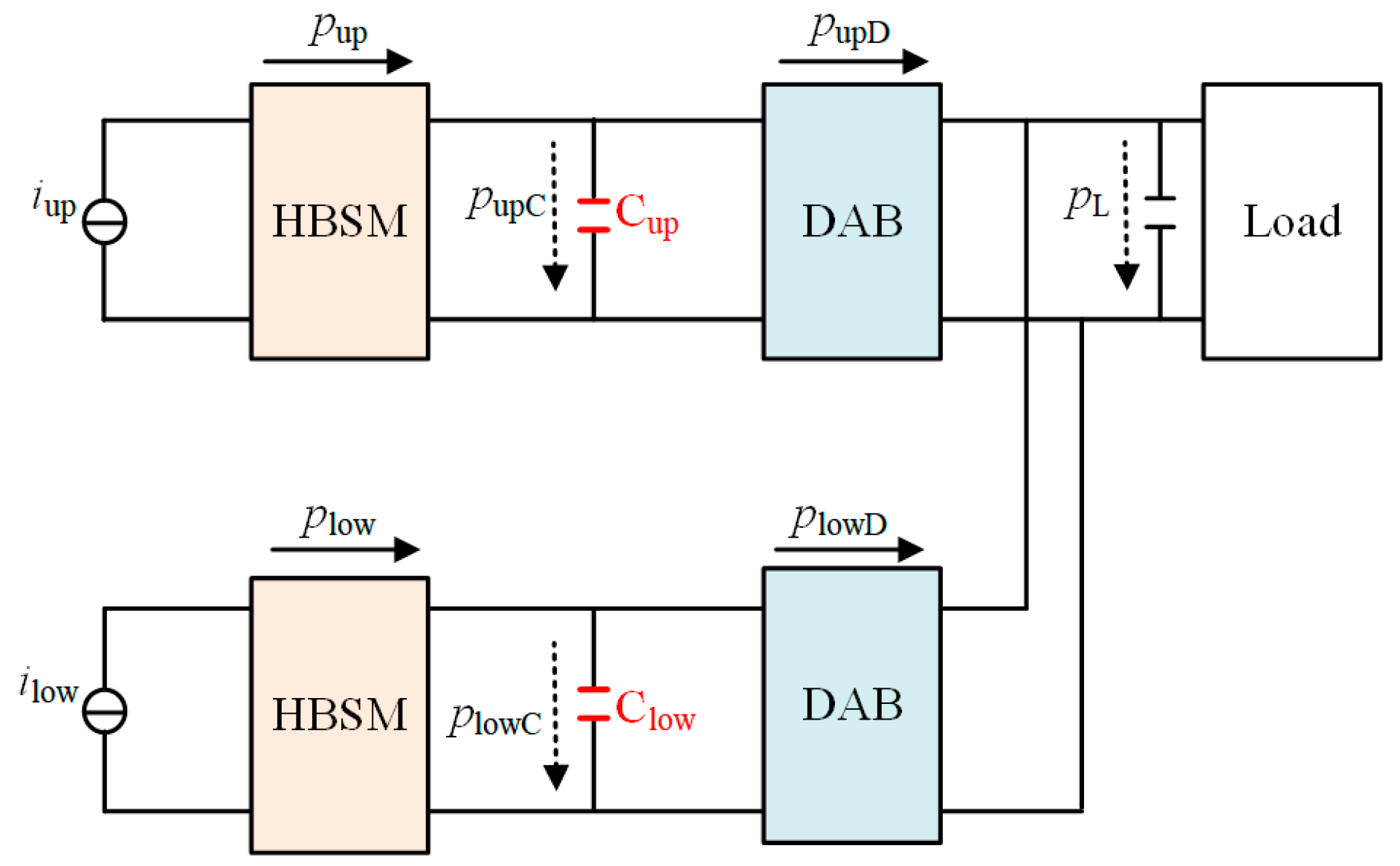
To facilitate the analysis of power flow characteristics between the HBSM and DAB, power transmission schematic diagrams of the upper and lower arm submodules are presented. As shown in Figure 4, pupD and plowD denote the power flowing into the DAB from HBSM of the upper and lower arms, respectively; pupC and plowC represent the power flowing into the capacitors C; and pL denotes the power delivered to the LVDC bus. For the DC components in pup and plow, the capacitive impedance approaches infinity at DC. Consequently, these DC components are entirely transferred to the DAB. In contrast, the capacitive impedance is relatively low for the AC components, allowing only a portion of the AC components to reach the DAB, while the remainder is absorbed by the capacitor. This diversion of AC components to the capacitor Cup (Clow) inevitably generates voltage ripple across it, which will be analyzed in detail in the following section.
Assuming that the proportion of the AC component transmitted to the DAB is denoted by ξ, then pupD and plowD can be mathematically expressed as follows:
p upD = p ¯ up + ξ p ˜ up p lowD = p ¯ low + ξ p ˜ low 0 ξ 1
where p ¯ up , p ˜ up , p ¯ low and p ˜ low denote the DC and AC components of pup and plow, respectively.
Furthermore, the AC power across capacitors Cup and Clow is obtained:
p ˜ upC = ( 1 ξ ) p ˜ up p ˜ lowC = ( 1 ξ ) p ˜ low 0 ξ 1
Based on the principle of instantaneous power conservation, the following relationship can be derived:
p ˜ upC C u ¯ C _ up d u ˜ C _ up d t
where u ¯ C _ up represents the DC component of the capacitor voltage, while u ˜ C _ up corresponds to its AC component.
Furthermore, the instantaneous voltage across the capacitor in the upper arm can be expressed as derived in Equation (15). Similarly, the instantaneous voltage across the capacitor in the lower arm is given by Equation (16).
u ˜ C _ up ( t ) = U peak V I ( 1 ξ ) ( π 3 θ ) [ cos ( 3 θ φ ) + 5 cos ( 3 θ + φ ) ] 5 3 CN π u ¯ c _ up ω , θ [ 0 , 2 π 3 ]
u ˜ C _ low ( t ) = U peak + V I ( 1 ξ ) ( π 3 θ ) [ cos ( 3 θ φ ) + 5 cos ( 3 θ + φ ) ] 5 3 CN π u ¯ c _ low ω , θ [ 0 , 2 π 3 ]
By applying Fourier expansion to Equations (15) and (16), the corresponding frequency-domain representations can be obtained:
u ˜ C _ up ( t ) c 0 c 1 cos ( 3 ω t ) d 1 sin ( 3 ω t )
u ˜ C _ low ( t ) c 0 + c 1 cos ( 3 ω t ) + d 1 sin ( 3 ω t )
where
c 0 = U peak + 24 V I ( 1 ξ ) sin ( φ ) 30 3 π CN u ¯ c _ up ω c 1 = 2 V I ( 1 ξ ) sin ( φ ) 5 3 π CN u ¯ c _ up ω d 1 = 3 V I ( 1 ξ ) cos ( φ ) 5 π CN u ¯ c _ up ω
As can be observed from Equations (17) and (18), a triple-frequency ripple voltage is generated across the capacitor. The magnitude of this ripple voltage is inversely proportional to the transmission ratio ξ. In other words, an increase in ξ results in a decrease in the triple-frequency ripple. Ideally, when ξ = 1, the triple-frequency ripple in the capacitor voltage disappears entirely.
However, the DAB operates in a high-frequency state and exhibits relatively high input inductive impedance [32], which significantly hinders the transmission of the AC component. Consequently, ξ tends to be small, indicating that the majority of the AC component from the HBSM will flow into the capacitor. To mitigate capacitor voltage fluctuations, a capacitor with a relatively large capacitance value is typically required.
Interestingly, increasing the transmission ratio ξ can reduce the capacitor voltage ripple, thereby allowing for a lower required capacitance value. To achieve this, this paper proposes using the TAB in place of the DAB. By applying the switched-capacitor principle to decrease the input inductive reactance and consequently increase the transmission ratio ξ, the capacitor voltage ripple can be effectively suppressed. The detailed analysis is presented as follows.

3. The Proposed TAB-Based MMDTC-PET

3.1. Topology Structure

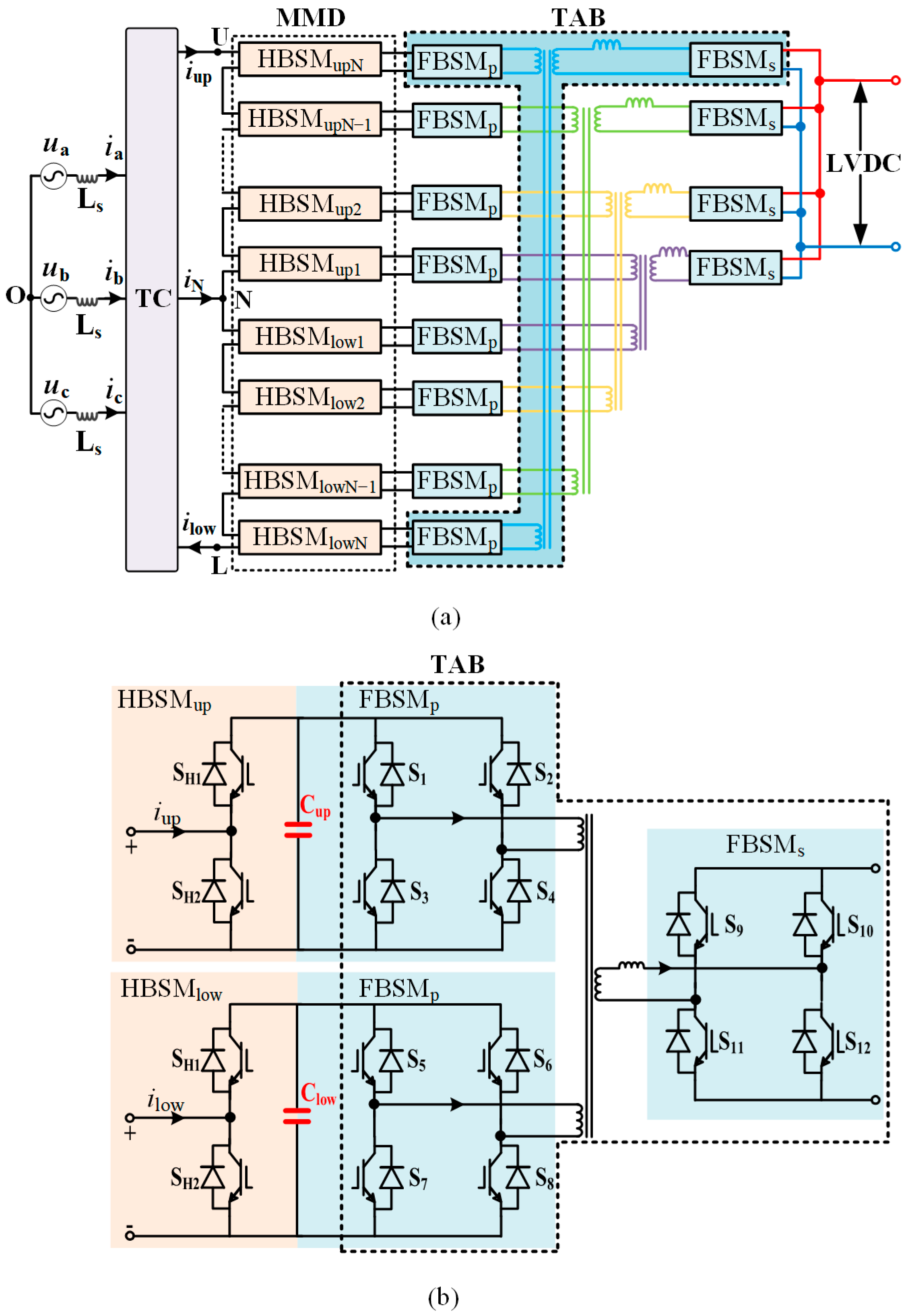
The topology of the TAB-based MMDTC-PET is illustrated in Figure 5. The TAB comprises two input ports and one output port. These input ports are, respectively, connected to a sub-module in the upper and lower arms, while the output port is linked to the LVDC.
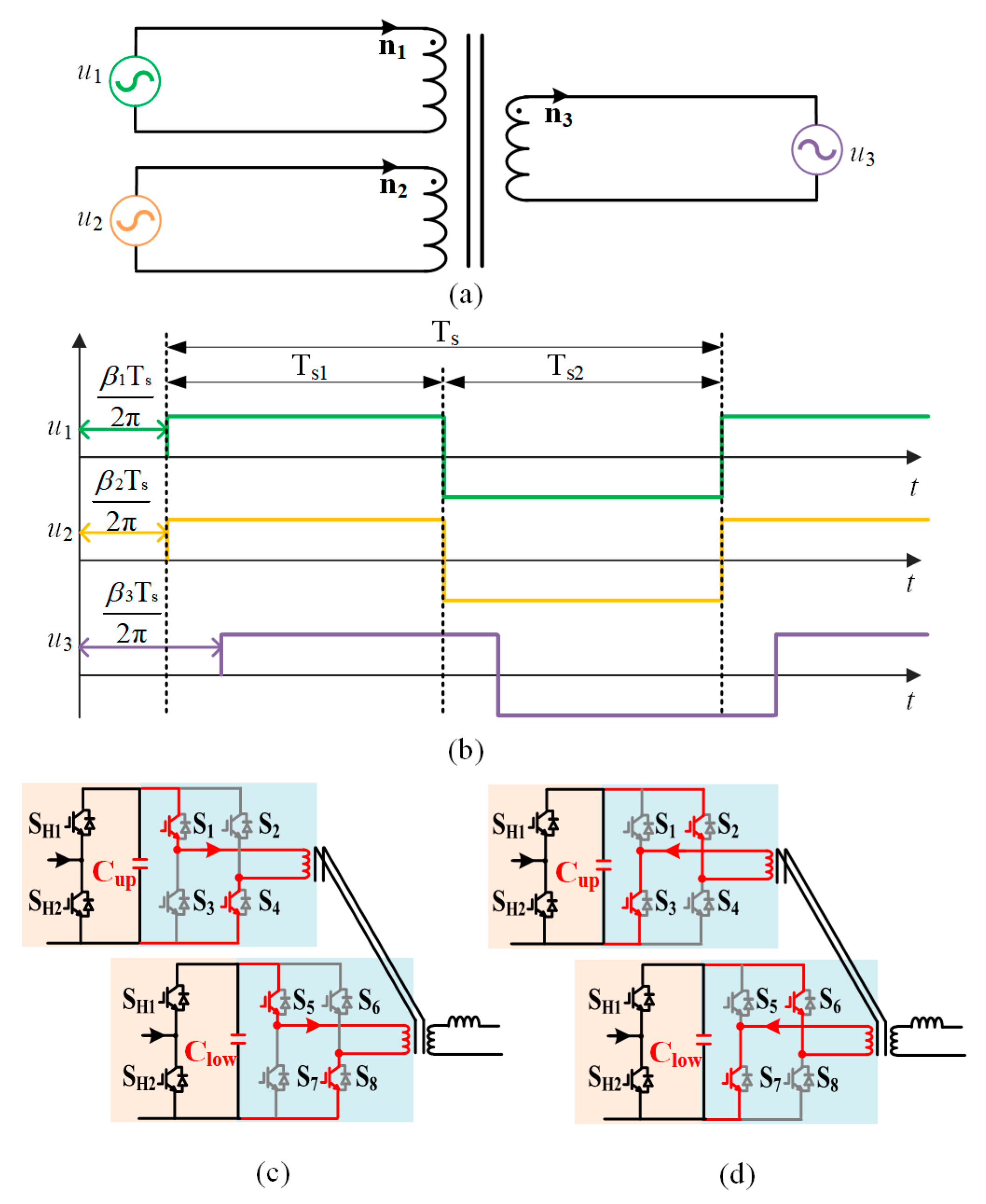
The equivalent model of the TAB is illustrated in Figure 6a. The two full-bridges at the input port of the TAB employ an identical phase-shift modulation strategy, as detailed in Figure 6b. Here, u1 and u2 represent the output voltages of these two full-bridge converters at the input port, respectively, while u3 denotes the output voltage at the output port. The phase angles of the modulation signals for the two input-side full bridges are denoted by β1 and β2, with β1 = β2. The phase angle of the modulation signal for the output-side full bridge is β3, and the phase-shift angle is defined as β = β3β1. By adjusting the magnitude of this phase-shift angle β, the power flow through the TAB can be effectively controlled.
All three full-bridge employ PWM modulation with a switching period of Ts and a duty cycle of 50%. During the first half of the switching period Ts1, the switching devices S1/S4 and S5/S8 are turned on. As a result, both input-side full-bridges output a positive voltage level, allowing the capacitors Cup and Clow to be directly connected in parallel. Similarly, during the second half of the switching period Ts2, the switching devices S2/S3 and S6/S7 are activated. Again, both input-side full bridges generate a negative voltage level, enabling Cup and Clow to be connected in parallel as illustrated in Figure 6c,d. Under high-frequency PWM modulation, Cup and Clow together form a switched-capacitor structure, enabling continuous charging and discharging between the two capacitors.

3.2. Analysis of the Voltage Ripple Suppression Principle

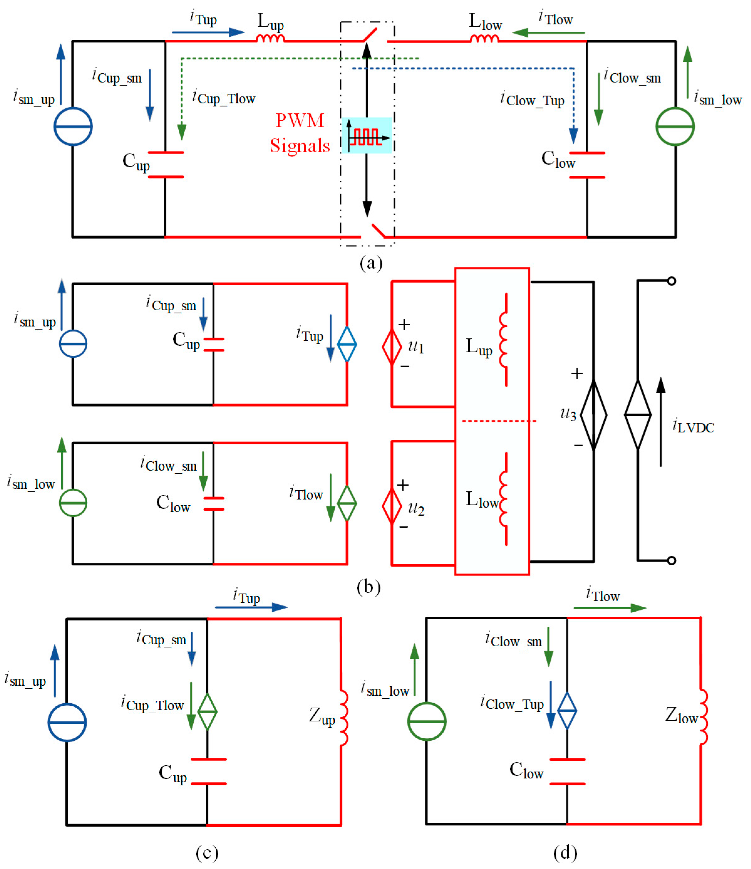
Figure 7a presents a schematic diagram of the current flow path in the switched-capacitor circuit, while Figure 7b illustrates the corresponding equivalent impedance model. In these diagrams, ism_up and ism_low denote the equivalent AC current sources representing the sub-modules. Due to the very low line impedance of the two capacitors connected in parallel, their voltages constrain each other and tend to equalize.
In the TAB, no external inductor is connected to the primary side of the transformer winding. However, the transformer winding inherently exhibits leakage inductance. Taking into account the influence of the transformer’s leakage impedance, Lup and Llow represent the leakage inductances of the transformers associated with the upper and lower arm sub-module.
Define the equivalent impedances of the upper and lower arm sub-modules as Zup and Zlow, respectively, as illustrated in Figure 7c,d. Taking the upper arm as an example, its equivalent input impedance with respect to the lower arm is:
Z up = Z Clow + Z Llow + Z Lup
where ZClow represents the capacitive impedance of the sub-module within the lower arm, and is expressed as ZClow = 1/jωClow. ZLup, ZLlow denote the inductive impedances associated with the leakage inductance, and are given by ZLup/low = jωLup/low.
The ripple currents of the sub-module capacitors in the upper and lower arms, originating from the equivalent AC current source input and the primary side of the TAB, are denoted as iCup/low_sm and iTup/low, respectively. Taking the upper arm as an example, based on the circuit’s equivalent model, the relationships among ism_up, iCup_sm, and iTup can be derived:
i sm _ up = i Cup _ sm + i Tup i Tup = i sm _ up . Z Cup Z Cup + Z up i Cup _ sm = i sm _ up . Z up Z Cup + Z up
In Figure 7a, the current flowing into the upper arm from the equivalent AC current source iTlow is denoted as iCup_Tlow. According to Kirchhoff’s Current Law (KCL), it can be obtained that iCup_Tlow = iTlow. Based on the superposition theorem and assuming that all sub-module capacitances and transformer parameters are identical, it follows that ZCup = ZClow = 1/jωC and ZLup = ZLlow = jωL, where C represents the capacitance and L denotes the leakage inductance. Under these conditions, the current iCup flowing through the capacitor can be expressed as:
i Cup = i Cup _ sm + i Cup _ Tlow = i sm _ up Z up Z Cup + Z up + i sm _ low Z Clow Z Clow + Z low = i sm _ up 1 1 1 ω 2 CL
Based on the fundamental relationship between voltage and current in a capacitor, the following expression can be derived:
d u ˜ C _ up d t = 1 ( 1 1 ω 2 CL ) CN u ¯ c _ up ω [ 6 3 V I cos ( φ ) 5 π cos ( 2 θ ) 4 3 V I cos ( φ ) 5 π sin ( 2 θ ) ] ,   θ [ 0 , 2 π 3 ]
Integrating the expression yields the voltage across the capacitor:
u ˜ C _ up = U peak + L V I ω ( π 3 θ ) [ cos ( 3 θ φ ) + 5 cos ( 3 θ + φ ) ] 5 3 N π u ¯ c _ up ( 1 CL ω 2 ) ,   θ [ 0 , 2 π 3 ]
when θ = 0, the valley value Uvalley is achieved. Let ∆ u ˜ C _ up = UpeakUvalley, that is:
Δ u ˜ C _ up = U peak U valley = 2 3 V I ω cos ( φ ) 5 N u ¯ c _ up ( 1 L C ω 2 )
As can be seen from Equations (22) and (25), the presence of leakage inductance L prevents the ripple current from being completely decoupled from the sub-module capacitor. However, by minimizing the leakage inductance during the design phase, its impact can be significantly reduced. Therefore, the leakage inductance L of the high-frequency transformer in the TAB is designed to be as small as possible, enabling icup to approach zero. This indicates that by utilizing the low-impedance characteristic of the switched-capacitor circuit’s equivalent connection, the fluctuating current ism_up is effectively decoupled from the sub-module capacitor and redirected to the secondary side of the high-frequency transformer at the TAB level, without requiring additional control for ripple power transfer.
Therefore, the ripple power transmission process can be equivalently described as follows: The AC components ism_up/low are transferred to the secondary side of the high-frequency transformer through the low-impedance path formed in the switched-capacitor circuit. Due to the characteristic that the amplitudes of the low-frequency ripple power in the upper and lower arms are equal while their phases are opposite, the ripple current that would otherwise flow into the sub-module capacitor cancels out on the common low-voltage DC bus, thereby eliminating its impact on the sub-module capacitor. As a result, only DC power flows into the LVDC bus, and the capacitor voltages of the sub-modules in both the upper and lower arms are mutually clamped, exhibiting only minor voltage ripples.
Therefore, the ripple power transmission process can be equivalently described as follows: The AC components ism_up/low are transferred to the secondary side of the high-frequency transformer through the low-impedance path formed in the switched-capacitor circuit. Due to the characteristic that the amplitudes of the low-frequency ripple power in the upper and lower arms are equal while their phases are opposite, the ripple current that would otherwise flow into the sub-module capacitor cancels out on the common LVDC bus, thereby eliminating its impact on the sub-module capacitor. As a result, only DC power flows into the LVDC bus, and the capacitor voltages of the sub-modules in both the upper and lower arms are mutually clamped, exhibiting only minor voltage ripples.

4. Simulation and Experimental Validation

4.1. Simulation Results

To verify the effectiveness of the proposed TAB in mitigating low-frequency voltage ripple across the capacitor, simulation models for both the DAB-MMDTC-PET and TAB-MMDTC-PET systems were developed using Simulink. The detailed simulation parameters are provided in Table 1.
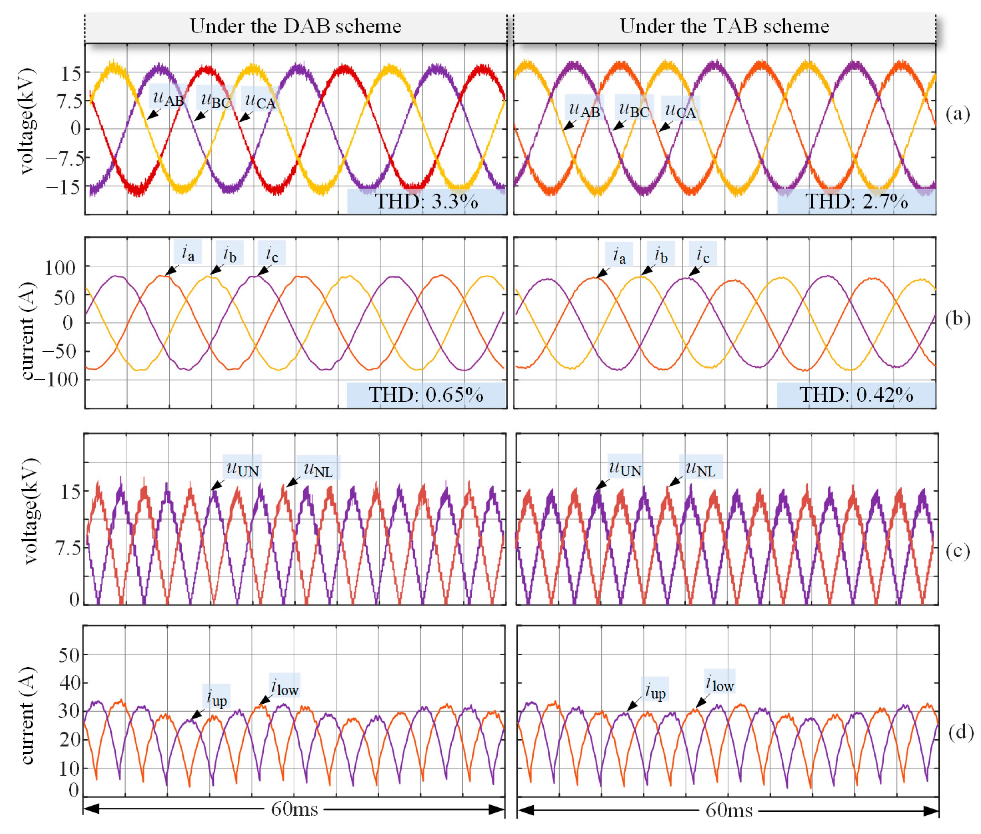
Figure 8a–d present comparative simulation results for both the conventional DAB scheme and the proposed TAB scheme, illustrating output line voltages, output currents, arm voltages, and arm currents. The results demonstrate that the fundamental operational characteristics of the MMDTC remain consistent regardless of the isolation stage configuration employed.
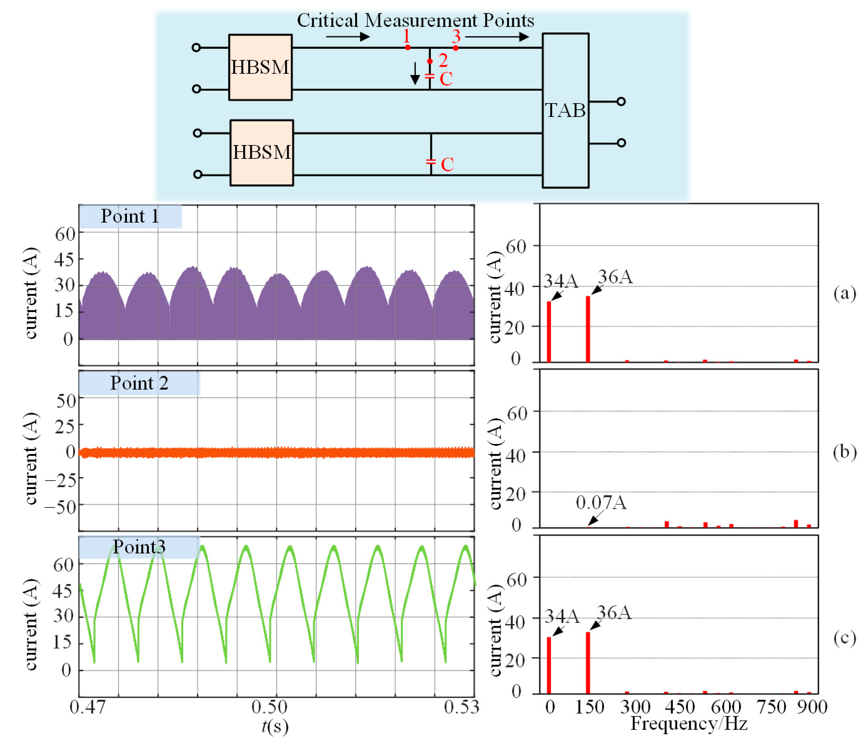
For the conventional DAB scheme, Figure 9 displays current waveforms and corresponding FFT analyses at three critical measurement points: The HBSM output, the sub-module capacitor input, and the DAB input. As shown in Figure 9a, the HBSM output current comprises a DC component of 34 A and a triple-frequency component of 36 A. Figure 9b,c reveals that the triple-frequency AC component predominantly flows into the sub-module capacitor, while the DC component is primarily transferred to the DAB input. These observations validate the theoretical analysis presented in Section 2.3.
For the proposed TAB scheme, Figure 10 presents current waveforms and FFT analyses at the corresponding measurement points. Comparing Figure 9a and Figure 10a, the DC and triple-frequency AC components at the HBSM output remain virtually identical. However, a dramatic reduction in the triple-frequency AC component is observed in the sub-module capacitor current when comparing Figure 9b and Figure 10b. This significant improvement results from the effective redirection of the triple-frequency AC component to the TAB, as evidenced in Figure 10c, demonstrating the successful implementation of the ripple power decoupling mechanism.
Figure 11 compares the capacitor voltages of all sub-modules in both upper and lower arms under the conventional DAB scheme and the proposed TAB scheme. The comparison clearly demonstrates that the sub-module capacitor voltage ripple ratio is dramatically reduced from 24% to 2.5% under identical operating conditions, validating the superior ripple suppression capability of the proposed TAB scheme.
Figure 12a–c illustrates the input and output port currents of the TAB along with their corresponding FFT analyses. The results reveal prominent triple-frequency components in both input ports with opposite phase relationships. Notably, the output port exhibits negligible triple-frequency content, confirming that the equal-amplitude, opposite-phase triple-frequency components from the two input ports effectively cancel at the output. This phenomenon validates the natural ripple cancelation mechanism inherent in the proposed topology.
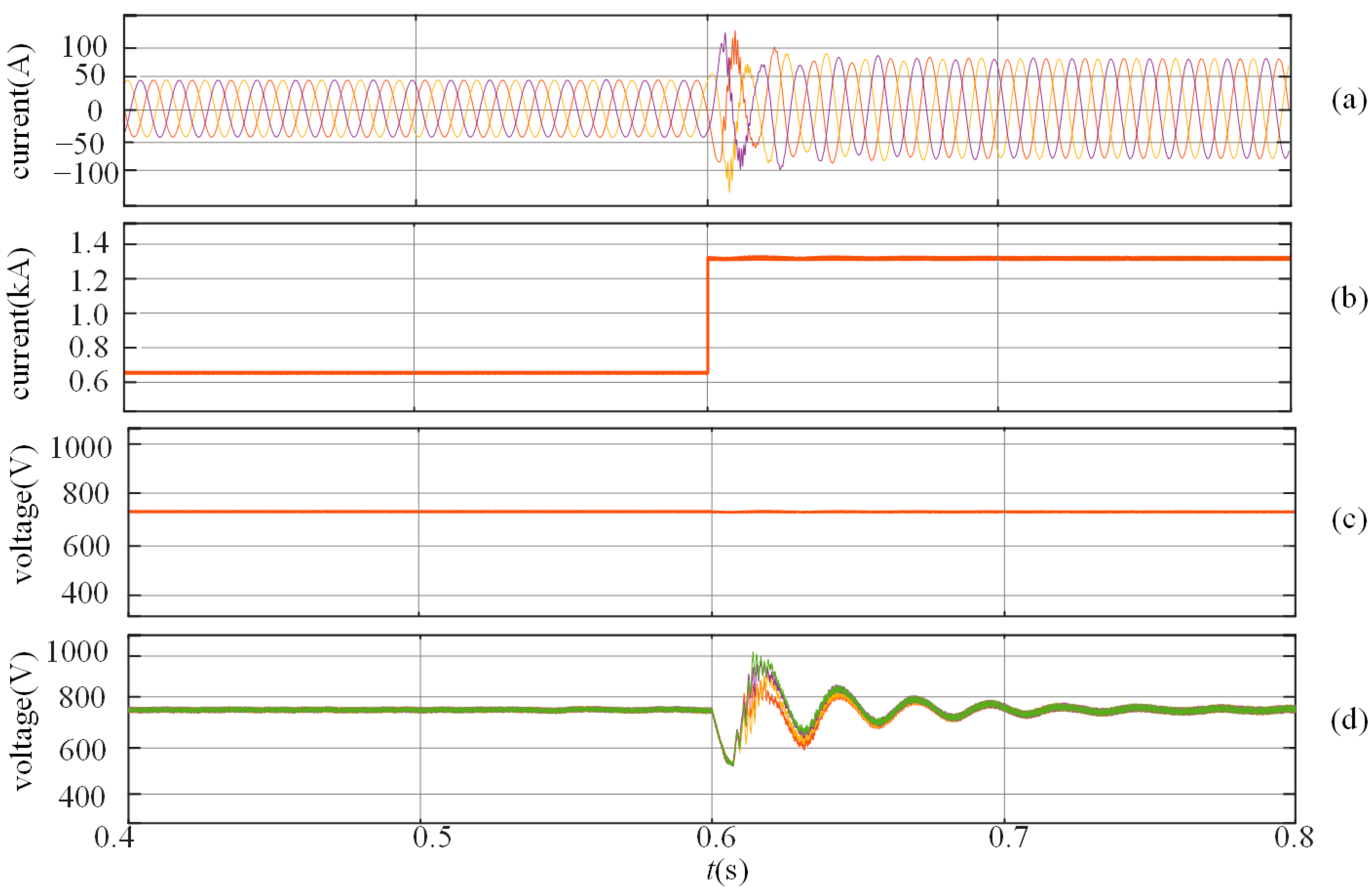
Figure 13 presents the system’s dynamic response under sudden load variations on the LVDC side. The results include three-phase grid-connected currents (Figure 13a), LVDC bus voltage and current (Figure 13b,c), and sub-module capacitor voltages (Figure 13d). The waveforms demonstrate rapid convergence to steady-state following the load disturbance, confirming the system’s robust dynamic performance and stability under transient conditions.
For a more intuitive comparison, this paper compares the hardware costs of using two DABs versus one TAB structure. Both topologies primarily consist of capacitors, IGBT devices, and high-frequency transformers.
In terms of capacitor cost, the submodule capacitor selection refers to Table 2(a), with the specific model being ALF80(1)122FP500 manufactured by KEMET. Assuming a capacitor voltage fluctuation ratio λ of 2.5%, the required capacitance values for the DAB and TAB schemes were calculated, with the results presented in Table 2(b). The selected capacitors have a rated voltage of 500 V and a nominal capacitance of 1.2 mF. In practical applications, series-parallel combinations are required to achieve the desired capacitance value. Compared to the DAB-based solution, the TAB structure reduces capacitor costs by approximately 87.5%, from $317.44 to $39.68.
Regarding switching device costs, the selected IGBT models are Infineon’s APTGL90H120T3G and FF50R12RT4HOSA1, with detailed parameters provided in Table 2(c). As shown in Table 2(d), since the current flowing through the secondary-side switching devices in the TAB topology is twice that of the primary side, secondary-side devices with double the rated current must be used. Ultimately, the total cost of switching devices is reduced by approximately 3%, from $971.2 to $936.8.
In terms of high-frequency transformers, the conventional DAB approach requires two independent transformers along with their associated magnetic components and control circuits. In contrast, the proposed TAB method uses only one three-winding transformer, effectively reducing the number of magnetic components while maintaining equivalent functionality.

4.2. Experimental Results

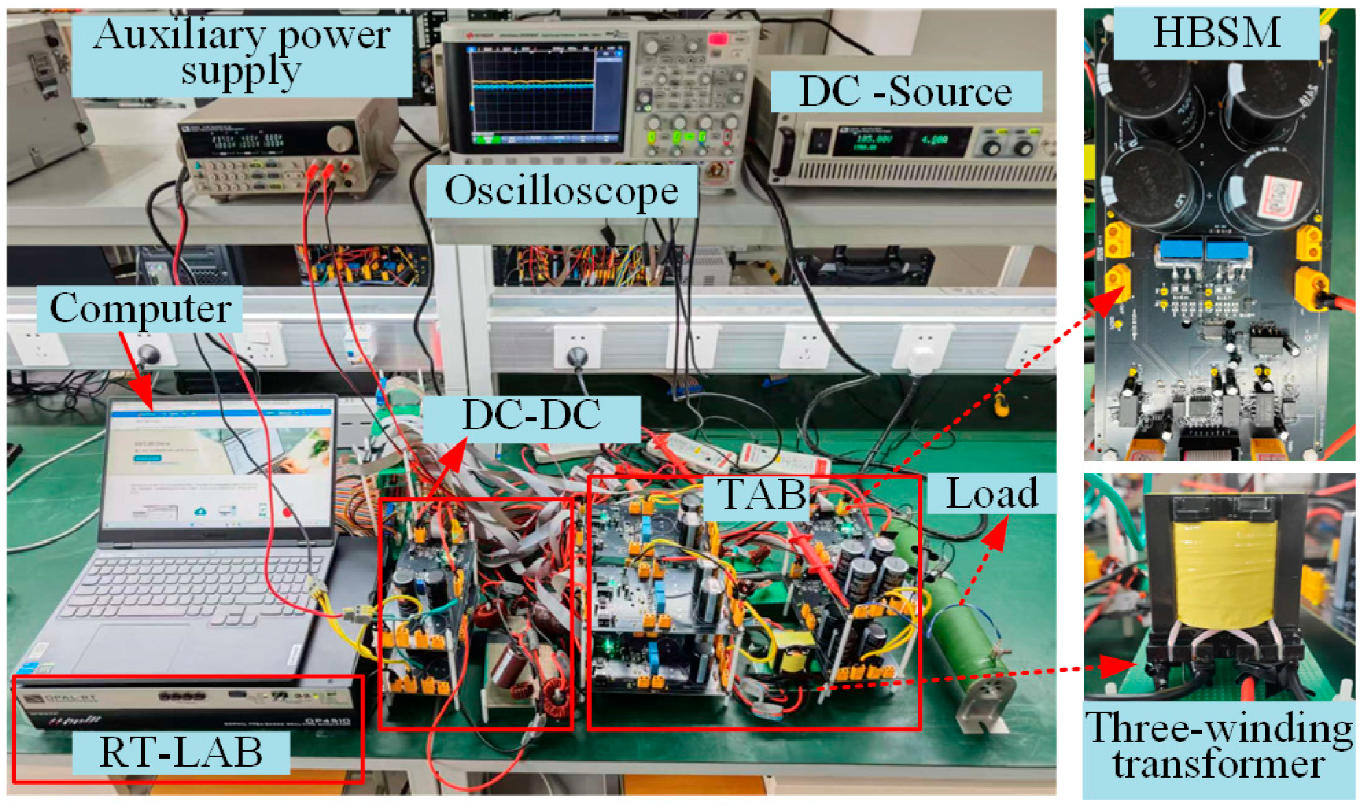
Due to the limitations of the power electronics experimental setup in our laboratory, constructing a complete TAB-based MMDTC-PET circuit is highly challenging. Consequently, a simplified experimental approach was adopted, as illustrated in Figure 14. Two DC-DC converters are utilized to emulate the triple-frequency power output of the upper and lower arm submodules in the MMDTC. Specifically, the PWM signals for the DC-DC converters are generated by comparing a modulation wave containing triple-frequency components with a triangular carrier wave. Furthermore, the amplitudes of these triple-frequency components are identical in both modulated waves, but their phases are opposite. The prototype of the experimental platform is illustrated in Figure 15, where RT-LAB serves as the controller and the detailed experimental parameters are summarized in Table 3.
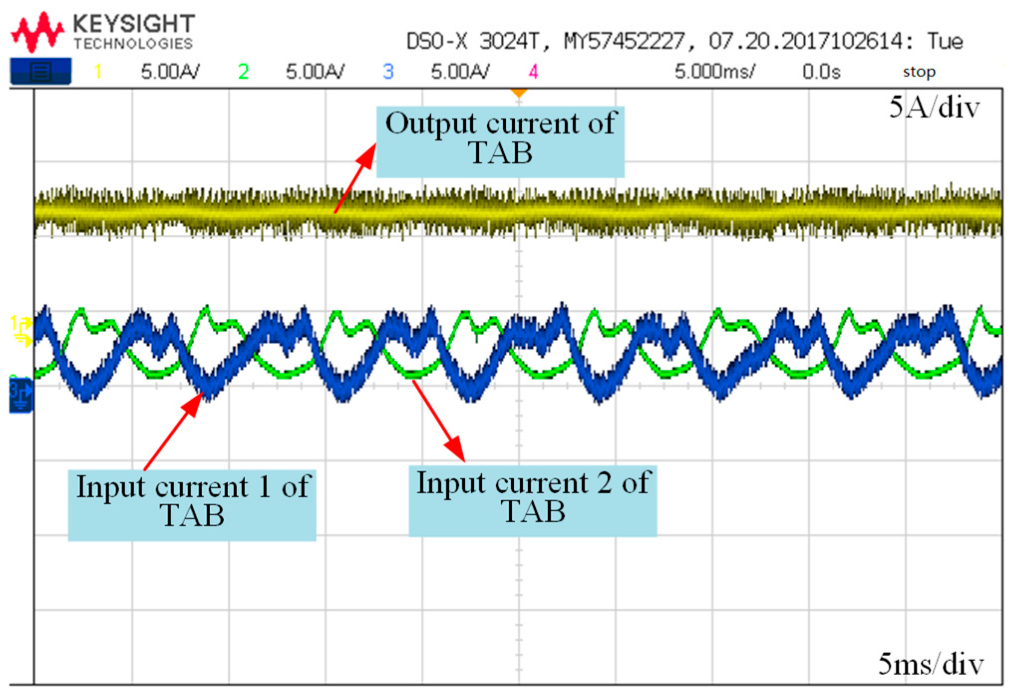
Figure 16 presents the current waveforms at the three critical measurement points—1′, 2′, and 3′—as shown in Figure 14, along with their corresponding FFT analyses. The current at each measurement point represents the DC-DC converter output current, the capacitor input current, and the TAB input current, respectively. The FFT results demonstrate that the majority of triple-frequency components present in the DC-DC output current are directed toward the TAB, whereas the capacitor input current consists only of higher-order harmonics. Figure 17 illustrates the current waveforms at measurement points 2′, 4′, and 5′. The currents at points 2′ and 4′ correspond to the TAB input current, while the current at point 5′ represents the TAB output current. As shown in Figure 17, the input current to the TAB contains triple-frequency components with opposite phase relationships, whereas the output current is free from such triple-frequency fluctuations.
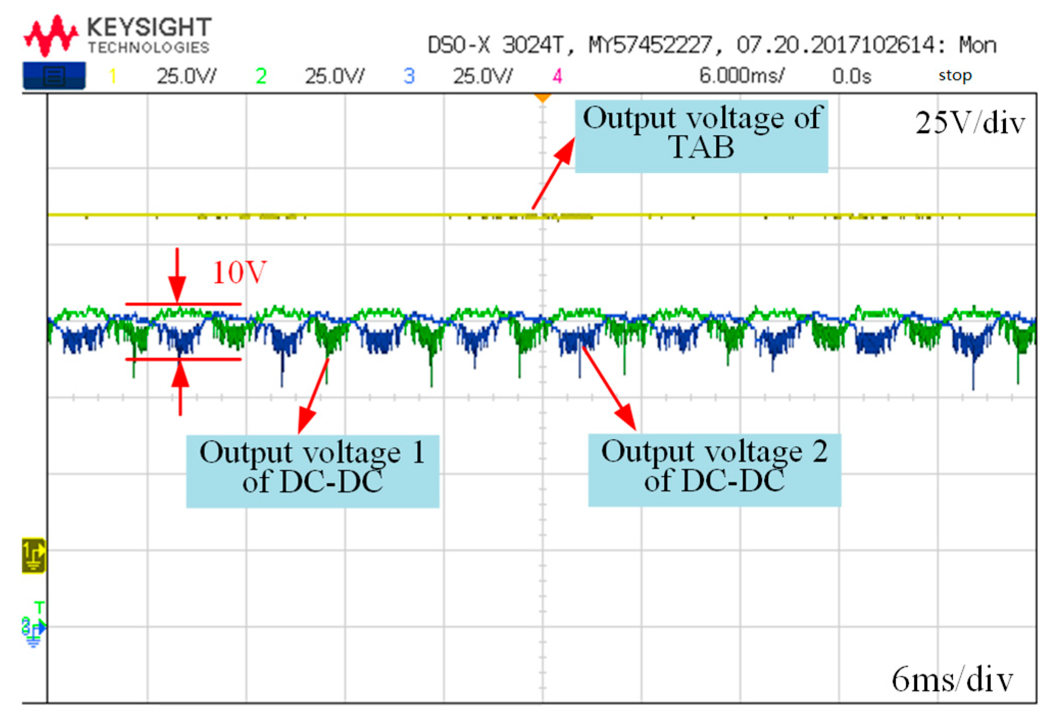
Figure 18 presents the output voltage waveforms of the DC-DC converter and the TAB output voltage. As shown, the output voltages of the two DC-DC converters exhibit triple-frequency ripple that are phase-opposed. The amplitude of the ripple voltage is 10 V, whereas the TAB output voltage remains consistently stable at 100 V. This indicates that, under the same phase modulation of the two full bridges on the primary side, the triple-frequency ripple component in the input current automatically cancels out on the output side due to the opposite phase characteristics of the triple-frequency components. Only the DC component is transferred to the output side of the TAB, which verifies the effectiveness of the TAB’s cancelation scheme for triple-frequency ripple.

5. Conclusions

This paper proposes a novel TAB-based MMDTC-PET topology to effectively suppress sub-module capacitor voltage ripple. By replacing conventional DABs with TABs and employing identical phase-shift modulation for the two primary-side full bridges, the proposed scheme creates a switched-capacitor configuration that provides a low-impedance path for ripple power. The theoretical analysis reveals that this configuration enables the redirection of triple-frequency AC components away from sub-module capacitors to the TAB secondary side, where they naturally cancel due to their equal-amplitude, opposite-phase characteristics in upper and lower arms. Simulation results demonstrate that the proposed method reduces capacitor voltage ripple from 24% to 2.5%.

Author Contributions

Conceptualization, X.C.; Methodology, X.C. and D.N.; Software, X.C., D.N. and Q.Y.; Validation, X.C., Q.Y. and D.W.; Formal analysis, D.W.; Investigation, Z.L.; Data curation, Z.L. and L.Z.; Writing—original draft, Q.Y. and D.W.; Writing—review & editing, X.C. and D.N.; Visualization, D.W.; Funding acquisition, D.W. All authors have read and agreed to the published version of the manuscript.

Funding

This work is supported by the National Natural Science Foundation of China (52407113); Natural Science Foundation of Shandong Province (ZR2024ME075), and Enterprise Project: Research and Development of Multilevel Converter for Integrated New Energy Power Generation and Energy Storage (kj20250221).

Data Availability Statement

The original contributions presented in this study are included in the article. Further inquiries can be directed to the corresponding author.

Conflicts of Interest

The authors declare no conflict of interest.

References

  1. She, X.; Huang, A.Q.; Burgos, R. Review of Solid-State Transformer technologies and their application in power distribution systems. IEEE J. Em. Sel. Top. P. 2013, 1, 186–198. [Google Scholar] [CrossRef]
  2. Sun, X.; Teng, J.; Qi, L.; Pan, Y.; Bu, Z.; Zhang, M. Research on triple-port MMC-Based PET scheme based on high frequency links interconnection of horizontal sub-modules. In Proceedings of the 2020 IEEE 9th International Power Electronics and Motion Control Conference (IPEMC2020-ECCE Asia), Nanjing, China, 29 November–2 December 2020. [Google Scholar]
  3. Li, F.; Li, Q.; Zhang, J.; Kou, J.; Ye, J.; Song, W. Detection and diagnosis of data integrity attacks in solar farms based on multilayer long short-term memory network. IEEE Trans. Power Electron. 2021, 36, 2495–2498. [Google Scholar] [CrossRef]
  4. Huber, J.E.; Kolar, J.W. Solid-State Transformers: On the origins and evolution of key concepts. IEEE Ind. Electron. M. 2016, 10, 19–28. [Google Scholar] [CrossRef]
  5. Dannier, A.; Rizzo, R. An overview of power electronic transformer: Control strategies and topologies. In Proceedings of the International Symposium on Power Electronics Power Electronics, Electrical Drives, Automation and Motion, Sorrento, Italy, 20–22 June 2012. [Google Scholar]
  6. Moghaddam, I.N.; Chowdhury, B.; Doostan, M. Optimal sizing and operation of battery energy storage systems connected to wind farms participating in electricity markets. IEEE T. Sustain. Energ. 2019, 1, 1184–1193. [Google Scholar] [CrossRef]
  7. Yu, Y.; Konstantinou, G.; Hredzak, B.; Agelidis, V.G. Power balance of cascaded H-Bridge multilevel converters for large-scale photovoltaic integration. IEEE Trans. Power Electron. 2016, 31, 292–303. [Google Scholar] [CrossRef]
  8. Heinemann, L. An actively cooled high power, high frequency transformer with high insulation capability. In Proceedings of the Seventeenth Annual IEEE Applied Power Electronics Conference and Exposition (Cat. No.02CH37335), Dallas, TX, USA, 10–14 March 2002. [Google Scholar]
  9. Briz, F.; Lopez, M.; Rodriguez, A.; Arias, M. Modular power electronic transformers: Modular multilevel converter versus cascaded H-Bridge solutions. IEEE Ind. Electron. M. 2016, 10, 6–19. [Google Scholar] [CrossRef]
  10. Guillod, T.; Krismer, F.; Färber, R.; Franck, C.M.; Kolar, W. Protection of MV/LV solid-state transformers in the distribution grid. In Proceedings of the IECON 2015—41st Annual Conference of the IEEE Industrial Electronics Society, Yokohama, Japan, 9–12 November 2015. [Google Scholar]
  11. Zhang, G.; Chen, J.; Zhang, B.; Zhang, Y. A critical topology review of power electronic transformers: In view of efficiency. Chin. J. Electr. Eng. 2018, 4, 90–95. [Google Scholar] [CrossRef]
  12. Niu, D.; Gao, F.; Xu, T.; Ma, Z. Thyristor-based T-type converter with modular multilevel DC-link. IEEE Trans. Power Electron. 2022, 37, 6792–6806. [Google Scholar] [CrossRef]
  13. Liu, S.; Niu, D.; Zhang, L.; Lin, J.; Fang, J.; Li, Z. Low-Capacitance operation and its hierarchical control for STATCOM based on T-Type converter with MMDTC. IEEE Trans. Power Electron. 2025, 40, 1153–1167. [Google Scholar] [CrossRef]
  14. Wang, R.; Wang, F.; Boroyevich, D.; Ning, P. A high power density single phase PWM rectifier with active ripple energy storage. IEEE Trans. Power Electron. 2011, 26, 1430–1443. [Google Scholar] [CrossRef]
  15. Li, H.; Zhang, K.; Zhao, H.; Fan, S.; Xiong, J. Active power decoupling for high-power single-phase PWM rectifiers. IEEE Trans. Power Electron. 2013, 28, 1308–1319. [Google Scholar] [CrossRef]
  16. Zhang, Y.; Fang, J.; Gao, F.; Gao, S.; Rogers, D.J.; Zhu, X. Integrated high- and low-frequency current ripple suppressions in a single-phase onboard charger for EVs. IEEE Trans. Power Electron. 2021, 36, 1717–1729. [Google Scholar] [CrossRef]
  17. Hu, Y.; Zhang, X.; Mao, W.; Zhao, T.; Wang, F.; Dai, Z. An optimized third harmonic injection method for reducing dc-link voltage fluctuation and alleviating power imbalance of three-phase cascaded H-Bridge photovoltaic inverter. IEEE Trans. Ind. Electron. 2020, 67, 2488–2498. [Google Scholar] [CrossRef]
  18. Hu, Y.; Li, Z.; Zhang, H.; Zhao, C.; Gao, F.; Luo, L.; Luan, K.; Wang, P.; Li, Y. High-frequency-link current stress optimization of cascaded H-Bridge-Based solid-state transformer with third-order harmonic voltage injection. IEEE J. Em. Sel. Top. P. 2021, 9, 1027–1038. [Google Scholar] [CrossRef]
  19. Isobe, T.; Barrera-Cardenas, R.A.; He, Z.; Zou, Y.; Terazono, K.; Tadano, H. Control of three-phase solid-state transformer with phase-separated configuration for minimized energy storage capacitors. IEEE J. Em. Sel. Top. P. 2020, 8, 3014–3028. [Google Scholar] [CrossRef]
  20. Liu, C.; Lai, J.-S. Low frequency current ripple reduction technique with active control in a fuel cell power system with inverter load. IEEE Trans. Power Electron. 2007, 22, 1429–1436. [Google Scholar] [CrossRef]
  21. Yin, X.; Luo, D.; Li, Z.; Su, Z. A method for secondary ripple voltage suppression in bidirectional isolated DC-DC converter. Trans. Electrotech. Soc. 2018, 33, 1356–1363. [Google Scholar]
  22. Wang, D.; Nahid-Mobarakeh, B.; Emadi, A. Second harmonic current reduction for a Battery-Driven grid interface with three-phase dual active bridge DC–DC converter. IEEE Trans. Ind. Electron. 2019, 66, 9056–9064. [Google Scholar] [CrossRef]
  23. Li, X.; Cheng, L.; He, L.; Zhu, Z.; Yang, Y.; Wang, C. Capacitor voltage ripple minimization of a modular three-phase AC/DC power electronics transformer with four-winding power channel. IEEE Access. 2020, 8, 119594–119608. [Google Scholar] [CrossRef]
  24. Pan, Y.; Teng, J.; Yang, C.; Bu, Z.; Wang, B.; Li, X.; Sun, X. Capacitance minimization and constraint of CHB power electronic transformer based on switching synchronization hybrid phase-shift modulation method of high frequency link. IEEE Trans. Power Electron. 2023, 38, 6224–6242. [Google Scholar] [CrossRef]
  25. Wang, Z.; Teng, J.; Zhang, M.; Bu, Z.; Lin, X.; Qi, L.; Zhao, W.; Li, X.; Sun, X. Common-Mode voltage suppression strategy for CHB-Based motor drive based on topology and modulation optimization. IEEE Trans. Power Electron. 2025, 40, 1697–1716. [Google Scholar] [CrossRef]
  26. Teng, J.; Sun, X.; Pan, Y.; Liu, X.; Zhang, Y.; Zhao, W.; Li, X. An inductive-filtering strategy of submodule ripple-power in triple-port MMC-Based SST applied to hybrid medium and low voltage AC/DC interface. IEEE Trans. Power Electron. 2022, 37, 8015–8032. [Google Scholar] [CrossRef]
  27. Xu, Y.; Tang, G.; Li, W.; Zhao, G.; Deng, Z. A three-phase integrated power electronic transformer with the capability of DC fault clearance. CSEE J. Power Energy Syst. 2021, 7, 785–796. [Google Scholar]
  28. Ma, Y.; Xiao, J.; Lin, H.; Wang, Z. A novel battery integration method of modular multilevel converter with battery energy storage system for capacitor voltage ripple reduction. IEEE Trans. Ind. Electron. 2021, 68, 12250–12261. [Google Scholar] [CrossRef]
  29. Pan, Y.; Teng, J.; Bu, Z.; Wang, J.; Yang, C.; Li, X.; Sun, X. A cascaded modular isolated back-to-back solid state transformer scheme for AC/DC/AC interconnection with improved performance and simple control. IEEE Trans. Power Electron. 2023, 38, 11050–11068. [Google Scholar] [CrossRef]
  30. Bu, Z.; Teng, J.; Sun, X.; Pan, Y.; Pan, Y. Low-frequency voltage ripples decoupling with switched-capacitor conversion for an MMC-Based SST. IEEE Trans. Ind. Electron. 2022, 69, 11293–11303. [Google Scholar] [CrossRef]
  31. Sun, X.; Teng, J.; Bu, Z.; Pan, Y.; Zhao, W.; Li, X. Research on triple-port SST Scheme based on the natural elimination of MMC submodule voltage fluctuation and imbalance. IEEE J. Emerg. Sel. Top. Power Electron. 2022, 10, 3697–3710. [Google Scholar] [CrossRef]
  32. Mueller, J.A.; Kimball, J.W. Model-based determination of closed-loop input impedance for dual active bridge converters. In Proceedings of the 2017 IEEE Applied Power Electronics Conference and Exposition (APEC), Tampa, FL, USA, 26–30 March 2017. [Google Scholar]
Figure 1. Schematic diagram of PET system with three stages.
Energies 18 05178 g001
Figure 2. Schematic diagram of (a) the DAB-based MMDTC-PET and (b) the detailed configuration of the connection between the HBSM and the DAB.
Energies 18 05178 g002
Figure 3. The relationship diagram illustrating the connections among arm voltages, three-phase line voltages, and switching states in the T-type structure.
Energies 18 05178 g003
Figure 4. Schematic diagram of the power transmission mechanism of DABs in the upper and lower arm.
Energies 18 05178 g004
Figure 5. Schematic diagram of (a) the proposed TAB-based MMDTC-PET and (b) the detailed configuration of the connection between the HBSMs and the TAB.
Energies 18 05178 g005
Figure 6. Schematic diagram of (a) equivalent model, (b) phase-shift modulation, (c) two capacitors connected in parallel during the first half cycle Ts1, and (d) two capacitors connected in parallel during the second half cycle Ts2 using the proposed TAB scheme.
Energies 18 05178 g006
Figure 7. Schematic diagram of (a) the simplified conduction path based on the switched-capacitor circuit, (b) the equivalent impedance model based on the switched-capacitor circuit, (c) the equivalent circuit from the perspective of the first input port, and (d) the equivalent circuit from the perspective of the second input port using the proposed TAB scheme.
Energies 18 05178 g007
Figure 8. Simulation results of (a) output line voltages, (b) output currents, (c) arm voltages, and (d) arm currents under the DAB scheme and proposed TAB scheme, respectively.
Energies 18 05178 g008
Figure 9. Current and its FFT analysis at (a) the output port of HBSM, (b) the input port of submodule capacitor, and (c) the input port of DAB. The arrow indicate the direction of current flow, and the numbers represent the sequence numbers of the measurement points.
Energies 18 05178 g009
Figure 10. Current and its FFT analysis at (a) the output port of HBSM, (b) the input port of submodule capacitor, and (c) the corresponding input port of TAB.
Energies 18 05178 g010
Figure 11. Comparison of all submodule capacitor voltages using (a) the DAB scheme and (b) the proposed TAB scheme, respectively.
Energies 18 05178 g011
Figure 12. Current and its FFT analysis at (a) the input port of the TAB in the upper arm, (b) the input port of the TAB in the lower arm, and (c) the output port of the TAB.
Energies 18 05178 g012
Figure 13. Simulation results showing (a) three-phase output current, (b) LVDC bus current, (c) LVDC bus voltage, and (d) all SM capacitor voltage waveforms under a sudden load change on the LVDC side.
Energies 18 05178 g013
Figure 14. Structural Composition of the Experimental Platform.
Energies 18 05178 g014
Figure 15. Photographs of the experimental prototype.
Energies 18 05178 g015
Figure 16. Experimental results of (a) the current waveforms observed at the measurement points 1′, 2′, and 3′, (b) FFT analysis of output current of DC-DC, (c) FFT analysis of input current of capacitor, and (d) FFT analysis of input current of TAB.
Energies 18 05178 g016
Figure 17. Experimental results of input current and output current of TAB.
Energies 18 05178 g017
Figure 18. Experimental results of the output voltage of DC-DC converter and the output voltage of TAB.
Energies 18 05178 g018
Table 1. The main parameters of simulation.
VariableSymbolValue
Rated grid phase voltageVg10 kV
AC filtering inductorLs2 mH
Rated active powerPrated1 MW
Fundamental frequencyf50 Hz
Number of SMs per armN20
Voltage of submodule capacitoruc750 V
Submodule capacitorC0.5 mF
Carrier frequencyfc10 kHz
LVDC bus voltageuLVDC750 V
DAB Transformer Turn Ration1:n21:1
TAB Transformer Turn Ration1:n2:n31:1:1
DAB additional inductorL25 μH
TAB additional inductorL25 μH
Switching frequencyfs40 kHz
Table 2. (a). Technical parameters list of capacitor. (b). Comparison results in terms of capacitor costs. (c). Technical parameters list of IGBTs. (d). Comparison results in terms of IGBT costs.
(a)
ModelCapacitanceCost PerNormal Voltage
ALF80(1)122FP5001.2 mF$19.84500 V
(b)
TypeDouble DABsSingle TAB
Capacitance required4.8 mF0.5 mF
Total Number of capacitors18 (Two in series and nine in parallel)2 (Two in series)
Total cost$317.44$39.68
(c)
ModelNormal VoltageCost PerRated CurrentSwitching Frequency
APTGL90H120T3G (IGBT)1200 V$112.8110 A20–50 kHz
FF50R12RT4HOSA1(IGBT)1200 V$60.750 A20–50 kHz
(d)
TypeDouble DABsSingle TAB
Total Number of IGBTs16(FF50R12RT4HOSA1)8(FF50R12RT4HOSA1) +
4(APTGL90H120T3G)
Total cost$971.2$936.8
Table 3. The main experimental parameters.
VariableSymbolValue
Rated active powerPrated500 W
Input voltage of DC-sourceU1105 V
Output voltage of TABU2100 V
LoadR20 Ω
PWM carrier frequencyfc10 kHz
Switching frequency fs10 kHz
Submodule capacitor C470 μF
TAB additional inductor L167 μH
Disclaimer/Publisher’s Note: The statements, opinions and data contained in all publications are solely those of the individual author(s) and contributor(s) and not of MDPI and/or the editor(s). MDPI and/or the editor(s) disclaim responsibility for any injury to people or property resulting from any ideas, methods, instructions or products referred to in the content.