Article

Online Junction Temperature Measurement for Power MOSFETs Using the Body Diode Under Varying Forward Currents

by
Xueli Zhu
1,
Yajie Huang
2,*,
Donglai Zhang
2,
Yuepeng Zhang
1,
Jun Wu
1,
Bowen Jiang
1,
Linzhong Xia
1,
Bo Gao
1 and
Changwei Lv
1
1
School of Sino-German Robotics, Shenzhen University of Information Technology, Shenzhen 518172, China
2
Power Electronics and Motion Control Research Center, Harbin Institute of Technology, Shenzhen 518055, China
*
Author to whom correspondence should be addressed.
Energies 2025, 18(19), 5045; https://doi.org/10.3390/en18195045
Submission received: 21 August 2025 / Revised: 12 September 2025 / Accepted: 19 September 2025 / Published: 23 September 2025
(This article belongs to the Special Issue Advancements in Power Electronics for Power System Applications)

Abstract

Power metal-oxide-semiconductor field-effect transistors (MOSFETs) provide numerous advantages and are widely utilized in various power circuits. The junction temperature plays a critical role in determining the reliability, performance, and operational lifetime of power MOSFETs. Therefore, accurate monitoring of the junction temperature of power MOSFETs is essential to ensure the safe operation of power circuit systems. In bridge or motor drive circuits, MOSFETs often operate in a freewheeling state via the body diode, where the freewheeling current is typically variable. The proposed method for junction temperature measurement utilizes the body diode and is designed to accommodate varying forward currents. It also accounts for the temperature-dependent ideality factor to improve measurement accuracy. By integrating the forward voltage and forward current of the body diode, this approach reduces the required sampling frequency. To validate the method’s effectiveness, three representative types of power MOSFETs, a Si MOSFET (IRF520), a SiC MOSFET (C2M0080120D), and an aerospace-grade radiation-hardened MOSFET (RSCS25045T1RH), were used to measure junction temperatures before and after irradiation. Following ideality factor correction, the maximum absolute error compared to reference measurements from thermocouples and a thermal imager remained within 2 K across the temperature range of 300 K to 420 K. Experimental results confirm the feasibility of the proposed method.

1. Introduction

Owing to their advantages, power MOSFETs have become widespread in various power electronics circuits, such as DC-DC converters, DC-AC converters, and motor drive circuits. The failure probability distributions of components in power electronic converters, as reported in various studies, are presented in Figure 1 [1,2,3,4,5,6,7]. Specifically, Figure 1a shows the distributions from references [1,2,3,4]; Figure 1b corresponds to the result provided in reference [5]; and Figure 1c displays the distribution given in reference [6,7]. Although different scholars provide varying probabilities of component failures in power electronic converters, MOSFETs consistently emerge as the weakest link, exhibiting a higher failure rate. Their performance critically impacts the healthy operation and service lifetime of power electronic converters. During operation, these components generate substantial heat from power losses, leading to significant temperature rise. High temperature fluctuations compromise device insulation, accelerating thermal aging. Over 50% of all failure factors of power semiconductor devices are attributed to overheating and junction temperature fluctuations, making these critical aspects of power semiconductor device failure [8]. The lifetime generally reduces by half when temperature increases by 10 °C [9]. Junction temperature substantially impacts the reliability, performance, and lifetime of power MOSFETs [10]. Therefore, accurate junction temperature measurement is essential for ensuring the safe operation of power electronics systems [11,12,13].
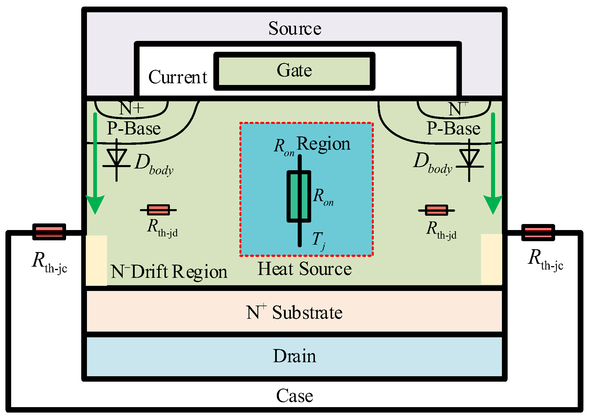
The junction temperature estimation methods for power MOSFETs can be systematically classified into four distinct categories: physical contact methods, optical methods, thermal network methods, and TSEP methods [14,15]. Physical contact and optical techniques enable direct temperature measurement, yet both require compromising the power MOSFET package structure. Moreover, the accuracy of thermal network models directly influences the precision of junction temperature monitoring, rendering real-time measurement challenging [16]. In contrast, the TSEP method facilitates noninvasive junction temperature measurement for power MOSFETs, making it a key research focus in this area [17,18]. The power MOSFET has a body diode between the source and drain terminals, where the forward voltage of this diode is inherently dependent on both junction temperature and forward current. As shown in Figure 2 [19,20], a typical power MOSFET structure consists of the Ron region operating in the first quadrant and the Dbody region functioning in the third quadrant. The body diode is an intrinsic structure situated closest to the chip’s junction region. Junction temperature measurement is achieved by utilizing the inherent relationship between its forward current, forward voltage, and temperature. This method eliminates the risk of detachment associated with external sensors and represents a highly reliable TSEP.
Commonly used TSEPs include the body diode forward voltage [21], the turn-on time [22], the turn-on saturation current [23], the dynamic threshold voltage [24], the on-state resistance [25], the on-state voltage [26,27], the turn-on delay time [28], the turn-off delay time [29], the current fall time [30], the turn-off miller plateau voltage [31], and the drain voltage falling edge time [32], etc. Notably, the body diode forward voltage demonstrates a negative temperature coefficient, while the on-state voltage exhibits a positive temperature coefficient [33]. Similarly, the drain-source current during turn-on transients shows excellent linear correlation with junction temperature, enabling accurate thermal characterization of power MOSFETs [14,34]. The integration of multiple TSEPs has been demonstrated to significantly enhance the accuracy and anti-interference ability of junction temperature measurement for MOSFETs [35]. A comprehensive comparison of the TSEPs for junction temperature measurement of power MOSFETs is summarized in Table 1. The performance of each TSEP was evaluated across four dimensions: sensitivity, linearity, aging effect, and integration capability. Here, “integration” refers to the ease with which the detection circuit can be incorporated into various power circuits.
The degradation of TSEPs in MOSFETs, caused by various electro-thermal stresses, is a well-established phenomenon [43]. Crucially, the relationship between TSEPs and junction temperature is altered by both gate-oxide degradation and packaging degradation. In power MOSFETs, gate oxide degradation primarily results from high electric fields and elevated junction temperatures [44], which causing shifts in threshold voltage, on-resistance, turn-on delay time, and turn-off delay time as the power MOSFET ages. Furthermore, the degradation of TSEPs can introduce significant measurement errors in junction temperature measurement [37]. Without correction for gate-oxide degradation, TSEP-based methods designed to be immune to packaging degradation exhibit reduced accuracy for MOSFETs [45,46]. A novel circuit design leveraging switching transients was proposed to provide an aging-compensated method for measuring the junction temperature of silicon carbide (SiC) MOSFETs [47]. By simultaneously measuring both turn-on and turn-off switching transients, this technique effectively mitigates the impact of device aging on online junction temperature measurement.
Furthermore, to avoid self-heating effects from high forward currents, junction temperature measurement typically employs a smaller sensing current [48,49]. Consequently, injecting an external low sensing current is often necessary when using the diode as a temperature sensor [38]. The body diode forward voltage is a reliable TSEP for accurate junction temperature measurement in power MOSFETs under low sensing currents [36,50]. Conventional diode-based temperature measurement methods, however, typically assume a constant ideality factor. It should be noted that this factor actually varies with temperature [51,52], leading to considerable measurement inaccuracies. In power electronic circuits, however, the high operating frequency of power MOSFETs results in extremely brief periods of freewheeling current flow through the body diode during switching. Consequently, measuring transient TSEPs at these high frequencies presents significant engineering challenges. For instance, the turn-off delay time is only a few hundred nanoseconds, making it difficult to capture. Existing junction temperature estimation methods suffer from drawbacks such as low resolution, complex installation requirements, and difficult implementation [53].
During the turn-off period of a MOSFET, its intrinsic body diode becomes forward-biased to sustain the inductive load current, thereby forming a transient current path, an operating condition referred to as the freewheeling state. In circuits such as bridges or motor drives, power MOSFETs frequently operate in a freewheeling state via the body diode, where the freewheeling current is often highly variable. The forward voltage of the body diode decreases when current flows through the channel of the power MOSFET. Therefore, to ensure accurate junction temperature measurement, the channel must be completely shut off to avoid interference from channel conduction. Unlike silicon (Si) MOSFETs, the precise fabrication of SiC devices makes the junction temperature measurement particularly sensitive to the gate-source bias voltage. Hence, applying a suitable negative gate-source bias is critical for obtaining accurate results. In [42], we proposed a junction temperature measurement method for power MOSFETs by processing the body diode forward voltage with compensation ideality factor. While effective under two fixed forward currents, this approach has limited applicability in practical scenarios where the body diode’s forward current typically varies.
To meet the requirements for online junction temperature measurement of MOSFETs under diverse operating conditions and to reduce the system sampling rate, we further propose a method operating under varying forward currents that significantly reduces the system’s sampling requirements. The method integrates the body diode’s forward voltage and current during operation, collecting the integrated data synchronously. This approach achieves accurate junction temperature measurement at a lower sampling frequency compared to transient-based TSEP methods. To overcome the limitation of a varying ideality factor, our method addresses by incorporating an experimentally derived relationship between ideality factor and temperature. This integration corrects measurement errors and delivers significantly higher precision.
This paper is organized as follows: Section 2 provides a theoretical analysis of the junction temperature for power MOSFETs. Section 3 presents the design of a junction temperature measurement system for power MOSFETs. Section 4 selects various power MOSFETs before aging as temperature sensors for experiments to verify the feasibility of the technique. Section 5 uses different power MOSFETs after irradiation as temperature sensors for experiments to validate the technique. Section 6 discussion the limitations regarding the practical implementation. Section 7 concludes this paper.

2. Theoretical Analysis of Junction Temperature Measurement for Power MOSFETs Using Body Diode Under Varying Forward Currents

It is necessary to directly utilize the varying forward current of body diode to achieve accurate measurement of the MOSFET junction temperature. The relationship between forward current and forward voltage for the body diode is expressed by Equation (1) [54].
i f = i s o e u f n k T j / q 1
where if is the forward current of the body diode, iso is the reverse saturation current of the body diode, uf is the forward voltage of the body diode, n is the ideality factor, k is Boltzmann’s constant, Tj is the junction temperature (in Kelvin), and q is the elementary charge.
Equation (1) is simplified to Equation (2) because of uf >> 0.
i f = i s o e u f n k T j / q
The reverse saturation current of the body diode, iso, varies at different temperatures since it is temperature-dependent. The impact of reverse saturation current eradicated by using two sensing currents, if1 and if2, to measure the temperature. Two time periods, Δt1 and Δt2, are designated to measure the junction temperature of power MOSFETs. The derivation process of the junction temperature measurement for the power MOSFET using body diode is as follows [55]:
i f 1 = i s o e u f 1 n k T j / q i f 2 = i s o e u f 2 n k T j / q
i f 1 i f 2 = e u f 1 u f 2 n k T j / q
u f 1 u f 2 = n k T j q ln i f 1 i f 2 = n k T j q ln i f 1 ln i f 2
where if1 and uf1 are the forward current and voltage within the period Δt1. if2 and uf2 are the forward current and voltage within the period Δt2.
u f 1 d t u f 2 d t = n k T j q ln i f 1 d t ln i f 2 d t
The integrated current over interval Δt1 is denoted as Ai1, and over Δt2 is denoted as Ai2. Similarly, the integrated voltage over Δt1 is denoted as Au1, and over Δt2 is denoted as Au2. Since the magnitude and waveform of the body diode’s forward current depend on the MOSFET’s operating conditions, Δt1 and Δt2 are consequently variable. The durations of Δt1 and Δt2 are related to the integral value of the forward current through the MOSFETs’ body diodes. In subsequent experimental verification, Δt1 and Δt2 were chosen to be unequal.
Defining A i 1 = ln i f 1 d t , A i 2 = ln i f 2 d t , A u 1 = u f 1 d t , A u 2 = u f 2 d t , we can rewrite Equation (6) as Equation (7). The junction temperature (Tj) of the power MOSFET is then expressed by Equation (8).
A u 1 A u 2 = n k T j q A i 1 A i 2
T j = q A u 1 A u 2 n k A i 1 A i 2
This ideality factor can be derived from Equation (8), as expressed in Equation (9).
n = q A u 1 A u 2 k T j A i 1 A i 2
Given that the body diode’s forward current characteristics vary with operating conditions in power MOSFETs, we propose a junction temperature measurement method utilizing this inherent forward current variability. Figure 3 illustrates the schematic of the forward current and forward voltage of the body diode based on its idealized characteristics, where both parameters undergo simultaneous processing.
The forward current of the body diode is composed of diffusion and drift current. The forward current density of the body diode can be expressed by Equation (10):
J f e q u f n k T j
where Jf is the forward current density of the body diode.
The ideality factor is a dimensionless parameter that quantifies the deviation of a diode’s behavior from ideal rectification, characterized by its role as a correction coefficient in the diode current-voltage equation. The ideality factor typically ranges between 1 and 2 [56]. At lower temperatures, diminished carrier diffusion causes this factor to approach 2 due to drift current dominance. Conversely, elevated temperatures enhance electron diffusion, increasing diffusion current and reducing the ideality factor toward 1 [57]. Consequently, the ideality factor varies with inconsistencies in the body diode’s forward current. The ideality factor of the body diode exhibits temperature dependence, with its variation trend being material-specific. For different body diode types, the ideality factor demonstrates an inverse correlation with temperature. Consequently, the expression of the ideality factor of body diodes with respect to temperature is given by Equation (11):
n = a T j + b T j + c
where coefficients a, b, and c are constants specific to the body diodes of power MOSFETs.
The ideality factor values at varying temperatures are determined experimentally. These coefficients in Equation (11) are extracted via the Levenberg–Marquardt algorithm.
Equation (8) is rewritten as Equation (12) by defining l = q A u 1 A u 2 / k A i 1 A i 2 .
T j = q A u 1 A u 2 n k A i 1 A i 2 = l n = l a T j + b T j + c
Solving Equation (12) yields the quadratic equation about temperature Tj as shown in Equation (13).
a T j 2 + b l T j l c = 0
Equation (13) is a quadratic equation that yields two solutions without constraints. However, in practical operation, the junction temperature of MOSFETs must be unique and cannot be lower than 0 K. Due to these physical limitations imposed by real-world operating conditions, it is necessary to discard the non-physical solution that contradict practical realities, thereby obtaining the correct junction temperature for the MOSFETs. Thus, the junction temperature of power MOSFETs measured by the body diode is expressed in Equation (14).
T j = b l + b l 2 + 4 a c l 2 a
Therefore, the value of *l* can be calculated using the body diode forward voltage and forward current measured during the two time periods, Δt1 and Δt2. Combining this with the constants a, b, and c related to the ideality factor of body diode, and applying Equation (14), the junction temperature of power MOSFET can be determined. To reduce the sampling frequency requirements for forward voltage and current, we implement simultaneous integration of these parameters. We also leverage the relationship between the ideality factor and temperature to enhance the accuracy of temperature measurement and refine the precision of the junction temperature measurements of power MOSFETs.

3. Online Junction Temperature Measurement System for Power MOSFETs

To validate the suitability of the proposed junction temperature measurement technique across the entire operating temperature range of power MOSFETs, it is crucial to employ a heating platform to heat the MOSFETs to various target temperatures. Since heating the MOSFETs within power electronic circuits directly using a heating platform is challenging, discrete devices are utilized for verification in this work. A voltage-controlled current source (VCCS) is configured to inject current into the MOSFET’s body diode to simulate the freewheeling state operation. Subsequently, the junction temperature is measured online using the proposed method.
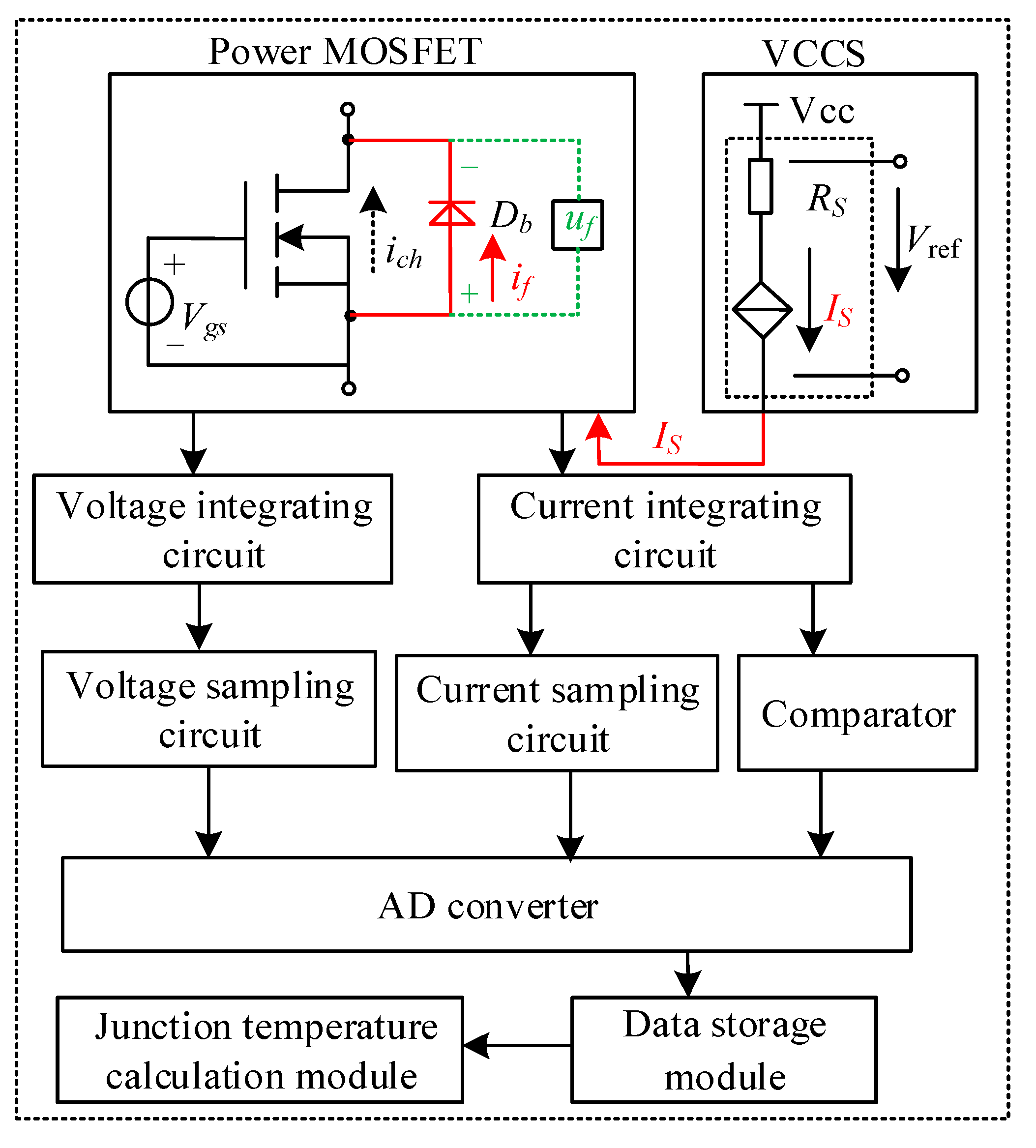
To measure the junction temperature of power MOSFETs, an online junction temperature measurement system was developed based on theoretical analysis. The system, illustrated in Figure 4, comprises the power MOSFETs to be tested, the VCCS, a voltage integrating circuit, a voltage sampling circuit, a current integrating circuit, a current sampling circuit, a comparator, an analog-to-digital (AD) converter, a data storage module, and a junction temperature calculation module. Within this setup, Db denotes the body diode of the power MOSFETs, Vgs represents the bias voltage between the gate and source of the power MOSFETs. IS signifies the sensing current produced by the VCCS, and its magnitude is determined by Vref and RS, simulating the forward current of the body diode. ich is the current flowing through the channel of the power MOSFETs, if is the forward current of the body diode, and uf represents the forward voltage of the body diode. When the channel of the power MOSFETs is closed, ich is equal to 0, and consequently, if is equal to IS under this condition.
The junction temperature measurement system for power MOSFETs operates by acquiring the body diode’s forward voltage through a voltage-integrating circuit, with its output captured by a voltage-sampling circuit. Similarly, a current-integrating circuit acquires the body diode’s forward current, and the circuit’s output is captured by a current-sampling circuit. Voltage and current data are synchronously sampled using an AD converter. Following this, the junction temperature calculation module computes the MOSFETs’ junction temperature. Owing to the high operating frequency of MOSFETs and the small forward voltage of the body diode, the accuracy of both the voltage and current integration circuits in the junction temperature measurement system, as well as the resolution of the digital-to-analog (DA) converter and AD converter, significantly influence the precision of junction temperature measurement in power MOSFETs. To enhance the temperature measurement accuracy and minimize the impact of noise interference, low input offset voltage operational amplifiers were employed in the design of the voltage and current integrators. Furthermore, to ensure high-resolution signal conversion, a 12-bit DA converter and a 16-bit AD converter (AD7606-4) with a 2 μs conversion time were selected, fully meeting the system’s response requirements.
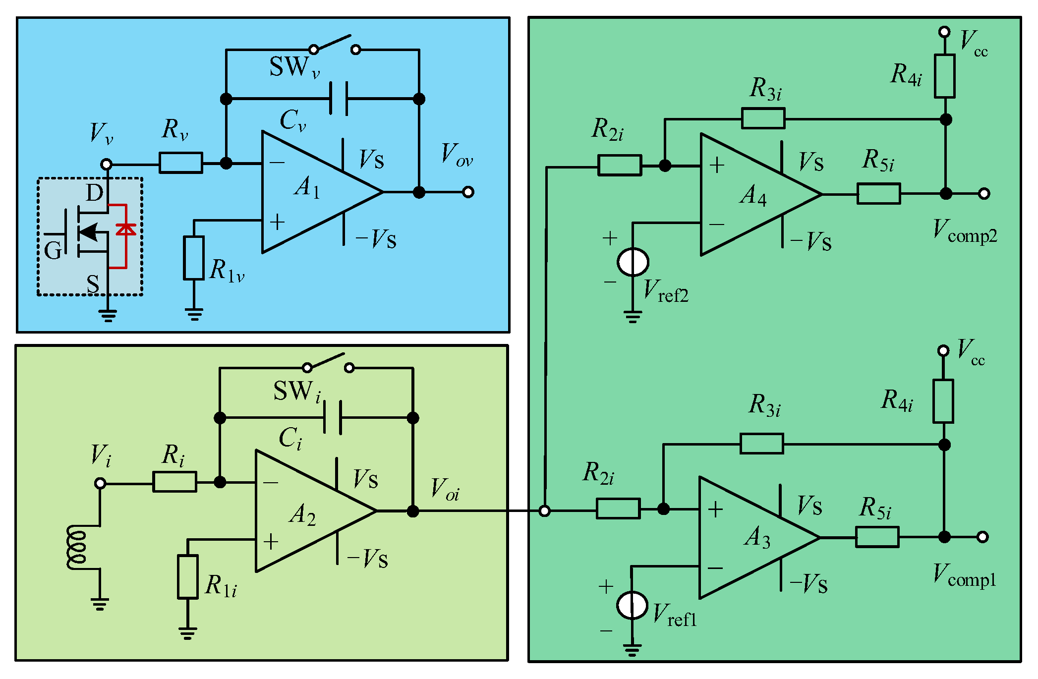
Figure 5 illustrates the body diode forward voltage and forward current processing circuit. Note that SWi and SWv serve as reset switches, enabling the discharge of the integrating capacitors through microcontroller control to reset the output result of the integrating circuits. Prior to each temperature measurement, the microcontroller provides a reset signal. The circuit in Figure 5 does not require recalibration to accommodate different types of MOSFETs. (Where Ri = 10 kΩ, Rv = 10 kΩ, R1i = 10 kΩ, R1v = 10 kΩ, R2i = 1 kΩ, R3i = 100 kΩ, R4i = 10 kΩ, R5i = 1 kΩ, Ci = 0.1 µF, Cv = 0.1 µF, vs. = 12 V, Vref1 = 1 V, and Vref2 = 3 V.) The capacitance and resistance parameters in the voltage and current integration circuits determine the integration time duration, which can be adjusted according to specific application requirements. Circuit precision was ensured through selective deployment of high-performance components including operational amplifiers, integration resistors, and AD converters. In the experimental setup, a capacitance value of 0.1 μF and a resistance value of 10 kΩ were employed, resulting in an integration time constant of 1 ms. Amplifiers A1 and A2 were implemented with high-precision operational amplifiers OP27, featuring a bandwidth of 8 MHz and an input offset voltage (Vos) of 10 μV. For A3 and A4, industrial-grade comparators LM239 were employed to meet the demanding requirements of high-accuracy junction temperature measurements.
The integrated output value of the forward voltage integrating circuit is expressed in Equation (15):
V o v = 1 R v C v 0 t V v d t + V 01
where V01 signifies the initial voltage of the integrating capacitor in the voltage integrating circuit, RvCv denotes the integral constant of the forward voltage integrating circuit, Vv represents the forward voltage of the body diode, Vov denotes the forward voltage integration value of the body diode, and t signifies the integration time.
The integrated output value of the forward current integrating circuit is expressed in Equation (16):
V o i = 1 R i C i 0 t V i d t + V 02
where V02 signifies the initial voltage of the integrating capacitor in the current integrating circuit, RiCi denotes the integral constant of the forward current integrating circuit, Vi represents the output voltage of the current sensor for the forward current of the body diode, Voi denotes the forward current integration value of the body diode, and t represents the integration time.
The comparator thresholds, Vref1 and Vref2, are set to trigger specific actions. When the integrated value of the forward current of the body diode reaches Vref1, the output signal of the comparator (Vcomp1) initiates the AD converter to simultaneously capture the output value of the voltage integrating circuit (Au1) and the output value of the current integrating circuit (Ai1). Similarly, when the integrated value of the forward current of the body diode reaches Vref2, the output signal of the comparator (Vcomp2) controls the AD converter to collect the output value of the voltage integrating circuit (Au2) and the output value of the current integrating circuit (Ai2) simultaneously. The junction temperature of the MOSFETs is then determined using the data collected by the AD converter.
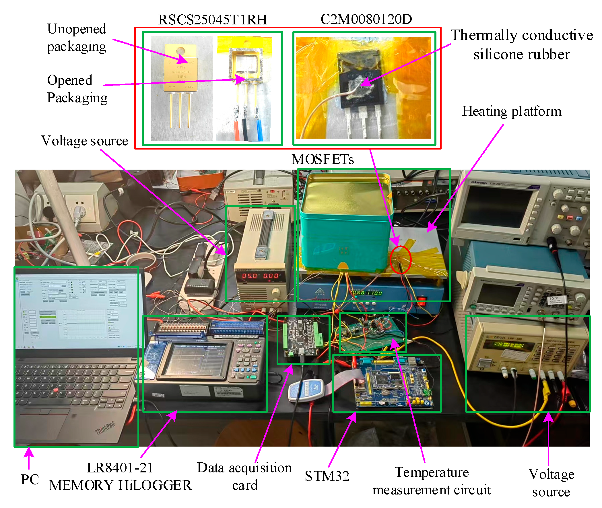
The experimental setup for measuring the junction temperature of power MOSFETs is illustrated in Figure 6. To authenticate the feasibility of the junction temperature computation, a heating platform (Model: JF-956E) with a temperature accuracy of 0.1 K was used to heat the power MOSFETs to various target temperatures. Thermally conductive silicone rubber is applied between the power MOSFETs and the heating platform, so that the heating platform can evenly heat the power MOSFETs to a specified temperature. Owing to differences in bandgap, switching characteristics, and packaging among various MOSFET devices, the temperature-dependent behavior of the body diode ideality factor varies significantly across different types [58,59]. Generally, both Si and SiC MOSFETs exhibit a decrease in the value of ideality factor with rising temperature, with the reduction being significantly more pronounced in SiC devices compared to their Si counterparts. In contrast, radiation-resistant MOSFETs demonstrate an increasing trend in the value of ideality factor as temperature elevates, accompanied by a more substantial variation. To comprehensively validate that the proposed junction temperature measurement method is applicable to various types of MOSFETs under varying forward currents, three representative devices were selected for experimental verification: a Si-based MOSFET (IRF520), a SiC MOSFET (C2M0080120D), and a radiation-resistant MOSFET (RSCS25045T1RH). According to the datasheets of three typical MOSFETs, the maximum operating temperatures are 423.15 K for the C2M0080120D, 448.15 K for the IRF520, and 423.15 K for the RSCS25045T1RH, while 300 K corresponds to room temperature. To ensure compatibility across all three devices, the upper temperature was selected to be close to the maximum operating limit of the C2M0080120D and RSCS25045T1RH, and the lower temperature was set to room temperature. Accordingly, the experimental temperature range was chosen to be from 300 K to 420 K. Variable forward currents are applied through the body diode, and then the junction temperature of the power MOSFETs is ascertained by processing the forward voltage under varying forward current.
Power MOSFETs such as the IRF520 and C2M0080120D typically employ plastic packaging. The plastic material encapsulates the semiconductor region of the MOSFET die, resulting in a package structure that is difficult to disassemble. Forced disassembly may damage the electrical structure of the MOSFET, causing physical degradation and functional failure. Unlike simulation models where the junction temperature of MOSFETs can be directly specified, experimental measurements capture only the surface temperature of the package rather than the internal junction temperature. Therefore, the heating platform serves as the thermal source for heating the power MOSFETs. Upon reaching the target temperature, this temperature is maintained for over 10 min to ensure thermal equilibrium between the internal and external regions of the MOSFETs. A thermocouple is affixed to the center of the MOSFET package surface using Setllon d3 high-temperature adhesive. Temperature data is recorded and displayed by an LR8401-21 MEMORY HiLOGGER with ±0.1 K accuracy. When thermal equilibrium is achieved within the MOSFET, the surface temperature measured by the thermocouple approximates the junction temperature. The acquired temperature reading represents a steady-state value, as the junction temperature in power MOSFETs is inherently spatially non-uniform. Therefore, thermocouple-based measurements were employed as a benchmark to validate the feasibility of the proposed method.
The experiment employs the RSCS25045T1RH MOSFET featuring a metallic package. Unlike plastic encapsulation, the drain, source, and gate of the MOSFET are encapsulated directly within a metal package, where the upper surface of the metal casing maintains no physical contact with the semiconductor die. Upon removal of the metal lid, the MOSFET die becomes fully exposed. Under this condition, to avoid disrupting normal device operation, the surface temperature distribution can be directly measured using an infrared thermal imager. The maximum temperature recorded on the die is regarded as the junction temperature of the MOSFET. Similarly, the heating platform served as the thermal source for heating the RSCS25045T1RH MOSFET. Upon reaching the target temperature, this state was maintained for over 10 min to ensure junction temperature stabilization. A thermal imager (HM-TPK20-3AQF/W) with ±2.0 K accuracy was then employed to directly measure the MOSFET junction temperature as a benchmark reference.

4. Experimental Verification of Junction Temperature Measurement for MOSFET Before Aging

The relationship between the ideality factor of the body diode and temperature is determined through experimental methods. This relationship is used to correct the temperature measurement and enhance the accuracy of junction temperature measurement for power MOSFETs. This study examines various types of power MOSFETs to validate the effectiveness of temperature measurement techniques using varying forward current. The proposed method is independent of the specific shape of the forward current, making it applicable in scenarios such as bridge converters or inverters where the freewheeling current of the body diode varies with the load. The method is also viable for constant current, which can be viewed as a special form of variable current. Therefore, the experimental validation only requires a variable current waveform to verify the feasibility of the proposed technique.

4.1. Experimental Verification of Junction Temperature Measurement for Si Power MOSFET

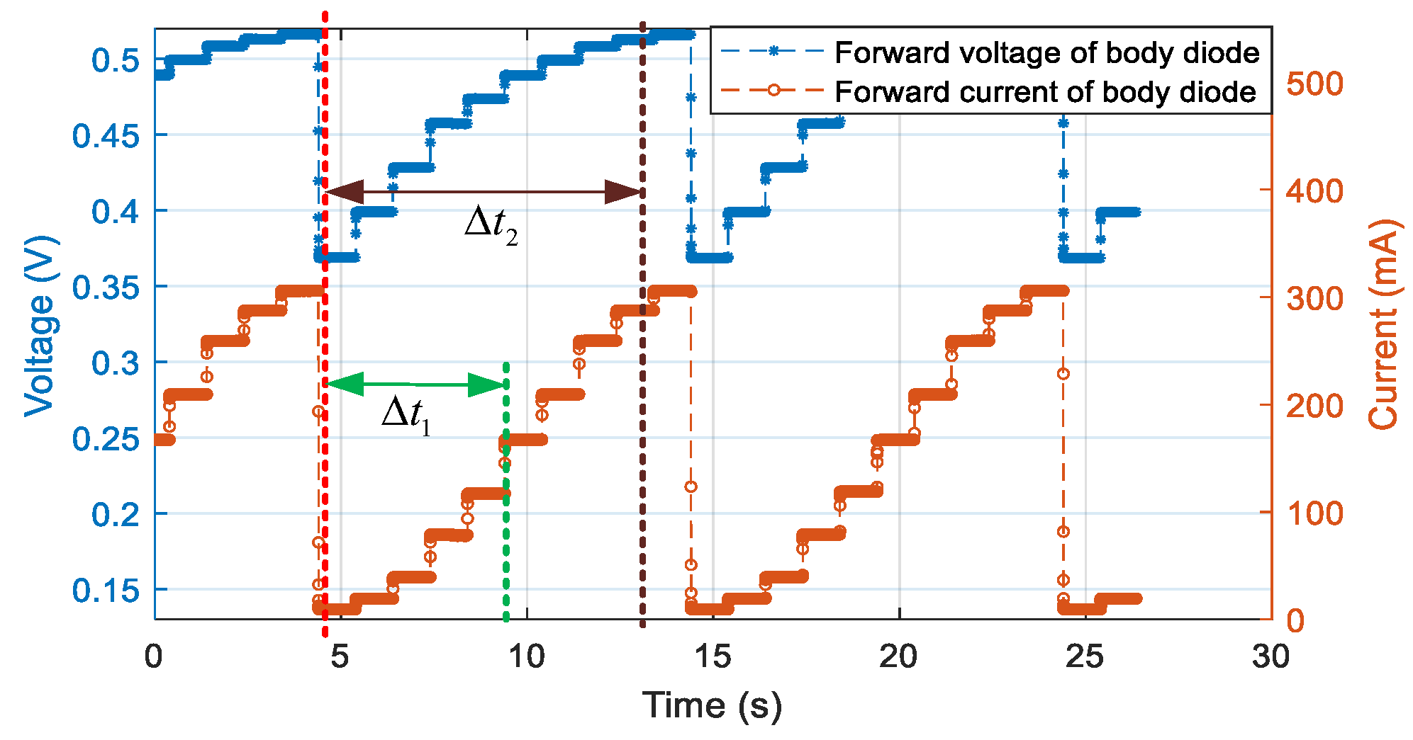
The technique described in this study aims to measure the junction temperature of power MOSFETs using the body diode. For this study, a commercially available 100 V, 9.2 A Si MOSFET (IRF520) from Onsemi is selected as the exemplary device to analyze the junction temperature measurement technique. A suitable bias of 0 V between the gate and source is applied to ensure the power MOSFET channel is completely closed. The sampling frequency used in all experiments is 1 kHz. To minimize errors introduced during the acquisition of the body diode forward voltage and forward current processing circuit, and to enhance the measurement accuracy of the junction temperature in MOSFETs, a sampling frequency of 1 kHz was adopted in this study. Additional forward current is applied to the body diode, and the corresponding forward current and forward voltage waveform with model IRF520 are illustrated in Figure 7.
The ideality factor at various temperatures is determined via experimental measurement. The model exhibits excellent agreement with experimental data of IRF520 (R2 = 0.9655), demonstrating strong correlation with Equation (11). The constants obtained using the Levenberg–Marquardt algorithm are a = 1.153, b = −217.9, and c = −192.6. The ideality factor and its corresponding fitting curve of the body diode in of IRF520 MOSFET are illustrated in Figure 8. By using the technique proposed in this study in conjunction with the constants obtained from the fitting curve, the junction temperature measurement absolute error obtained by the body diode in a power MOSFET is illustrated in Figure 9.
The absolute error in junction temperature measurement of IRF520 across the temperature range (300–420 K) with compensation for the ideality factor, is small. The absolute error in temperature measurement at each temperature point is within ±1 K, indicating the feasibility of the proposed method in this study.

4.2. Experimental Verification of Junction Temperature Measurement for SiC Power MOSFET

In this study, a commercially available 1.2 kV, 36 A SiC MOSFET (C2M0080120D) from Wolfspeed is selected as the exemplary device to analyze the junction temperature measurement technique. A negative bias of −5 V between the gate and source is applied to ensure that the channel of the power MOSFET is fully closed. Additional forward current is applied to the body diode, and the corresponding forward current and voltage waveforms with model C2M0080120D are presented in Figure 10.
The ideality factor was determined at various temperatures through experimental measurements. The model exhibits excellent agreement with experimental data of C2M0080120D (R2 = 0.9655), demonstrating strong correlation with Equation (11). The constants obtained through the Levenberg–Marquardt algorithm are a = 1.201, b = −320.2, and c = −270. The resulting ideality factor and its fitting curve for the body diode in the power MOSFET with model C2M0080120D are illustrated in Figure 11.
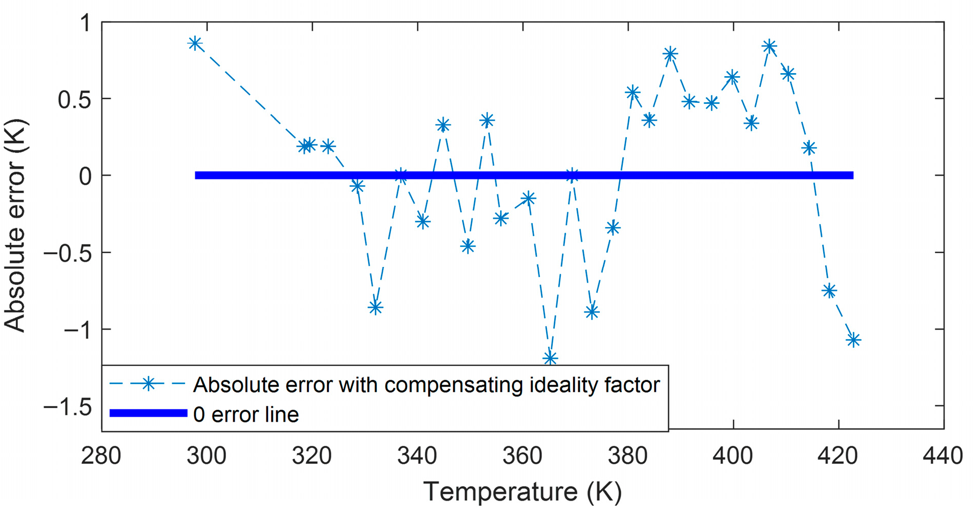
In conjunction with the constants derived from the fitting curve, the method proposed in this paper is utilized to obtain the temperature measurement absolute error from the body diode in a power MOSFET, as illustrated in Figure 12. The absolute error in junction temperature measurement for the C2M0080120D MOSFET remains within ±2 K across the temperature range from 300 K to 420 K when compensation for the ideality factor is applied, demonstrating the feasibility of the proposed technique.

4.3. Experimental Verification of Junction Temperature Measurement for Radiation-Resistant Power MOSFET

In this study, an aerospace-grade device with a 250 V, 45 A radiation-resistant power MOSFET (RSCS25045T1RH) is chosen as the representative device for analyzing the junction temperature measurement technique. During the experiment, the junction temperature of the RSCS25045T1RH MOSFET was controlled within the range of 300 K to 420 K. A suitable negative bias voltage of −5 V was applied between the gate and source terminals to ensure complete channel turn-off throughout testing. Following removal of the metal casing, the junction temperature was measured using an HM-TPK20-3AQF/W infrared thermography instrument. Figure 13 illustrates the thermal distribution across the MOSFET die at a stabilized temperature. The left panel shows the physical photograph of the device, while the right panel displays the temperature profile across different regions of the die. The temperature value indicated at the central crosshair (60.9 °C) represents the measured junction temperature. The forward current is applied to the body diode, and the forward current and voltage waveform with model RSCS25045T1RH are illustrated in Figure 14.
Table 2 summarizes the junction temperature measurement data for the RSCS25045T1RH, obtained using the proposed method. Based on the data presented in Table 2, the relationship between the ideality factor and temperature was fitted using Equation (11). The resulting model demonstrates excellent agreement with the experimental data of RSCS25045T1RH, as reflected by a high R2 value of 0.9884, indicating strong correlation with Equation (11). The parameters were optimized using the Levenberg–Marquardt algorithm, yielding the following values: a = 0.9452, b = −633.52, and c = −630.60. Figure 15 illustrates the ideality factor and its fitting curve for the body diode in a power MOSFET with model RSCS25045T1RH. Utilizing the approach proposed in this study and incorporating the constants obtained from the fitting curve, Figure 16 depicts the absolute error in temperature measurement obtained from the body diode in the power MOSFET.
It is observed that the junction temperature measurement’s absolute error for RSCS25045T1RH MOSFET within the temperature range of 300 K to 420 K is minimal. Moreover, the temperature measurement absolute error at each temperature remains below ±1.2 K, confirming the feasibility of the proposed method in this study.

5. Experimental Verification of Junction Temperature Measurement for Power MOSFET After Irradiation

The operation of a power MOSFET can lead to performance degradation and corresponding changes in the ideality factor of the body diode. The forward voltage of body diodes of power MOSFETs demonstrates superior stability and aging resistance compared to other TSEPs. This advantage makes body diodes optimal temperature sensors for MOSFETs junction temperature measurement. To further validate this methodology, radiation testing was performed on the MOSFETs. Cobalt-60 γ-ray irradiation was administered with a total ionizing dose (TID) of 23.5 krad(Si), simulating the radiation exposure experienced by aerospace-grade devices during normal operational cycles. Post-irradiation, junction temperature measurements were repeated and compared with pre-irradiation data. Comparative analysis confirmed the robustness of the body diode-based measurement technique under extreme environmental stress.

5.1. Experimental Verification of Junction Temperature Measurement for Si Power MOSFET After Irradiation

The power MOSFET with model IRF520 was irradiated with cobalt-60 γ-rays, leading to a total irradiation dose of 23.5 krad(Si). The ideality factors of the body diode at different temperatures were determined before and after the irradiation experiment, as presented in Figure 17. Following the experiment, the ideality factor of the body diode increased, showing varying changes across different temperatures. Notably, the change in the ideality factor of the body diode at low temperatures was more pronounced than at high temperatures. Recalibration of the ideality factor is necessary to ensure the accuracy of the junction temperature measurement of the power MOSFET.
The Levenberg–Marquardt algorithm yielded the corrected constants: a = 1.021, b = −97.39, and c = −138.7. Subsequently, the junction temperature of the power MOSFET was measured using these corrected parameters. The comparison of the absolute error in junction temperature measurement of the IRF520 before and after recalibrating the ideality factor is presented in Figure 18 following the irradiation experiment. Before recalibration, the absolute error in junction temperature measurement for IRF520 MOSFET was within 28 K, decreasing at higher temperatures. After recalibration, the absolute error for IRF520 MOSFET was reduced to within ±1.5 K, with most errors falling below ±1 K. This highlights the effectiveness of using the body diode for junction temperature measurement in power MOSFETs.

5.2. Experimental Verification of Junction Temperature Measurement for Radiation-Resistant Power MOSFET After Irradiation

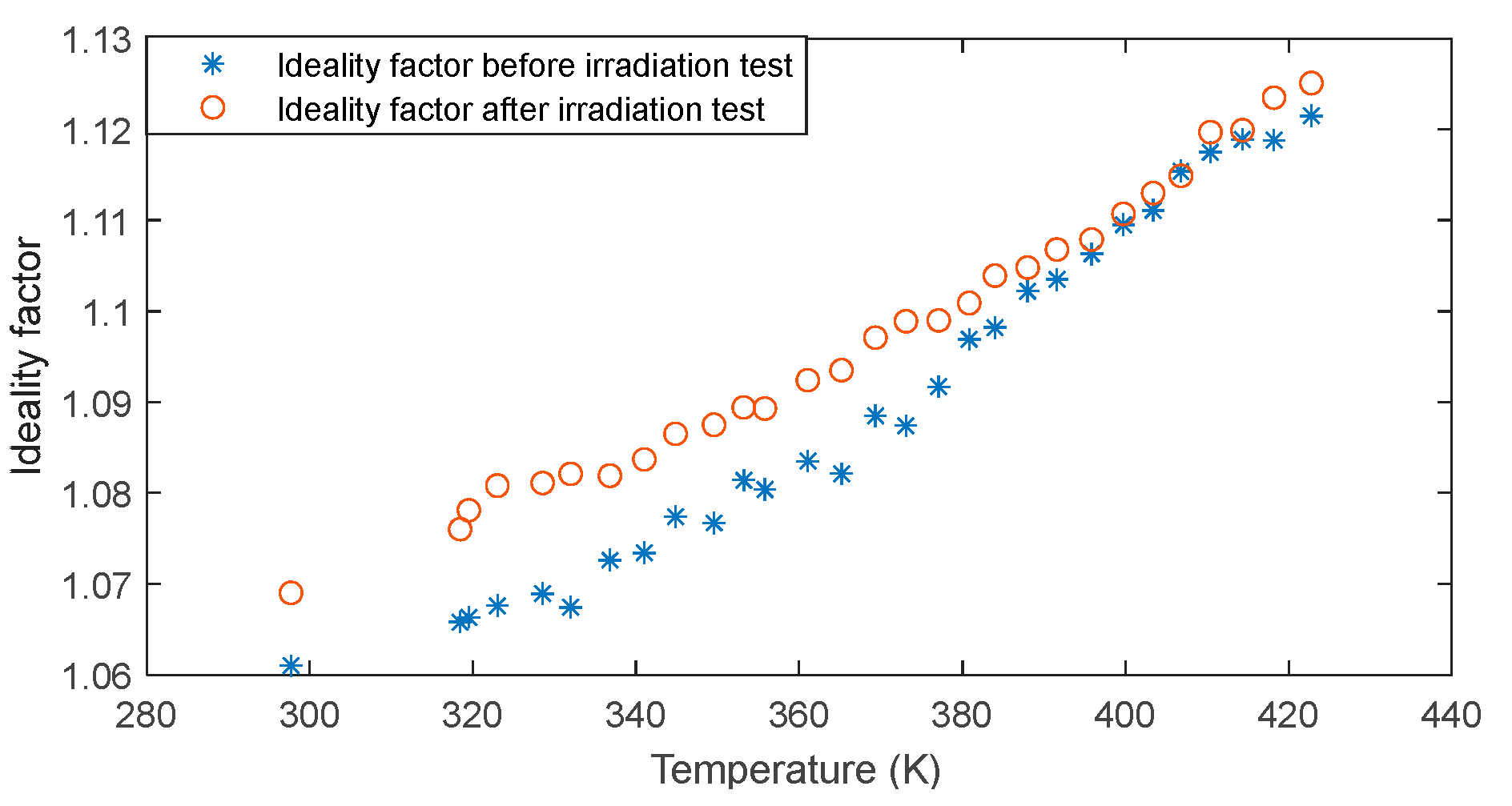
The power MOSFET with model RSCS25045T1RH was irradiated with cobalt-60 γ-rays, leading to a total irradiation dose of 23.5 krad(Si). The ideality factors of the body diode were measured at various temperatures before and after the irradiation experiment. The results, presented in Figure 19, show an increase in the ideality factor of the body diode after the irradiation experiment. However, the change in the ideality factor varies at different temperatures. Specifically, following irradiation with a total dose of 23.5 krad(Si), a significant increase in the ideality factors in the low-temperature range (300–380 K) was observed, while the ideality factors in the high-temperature range (380–430 K) remained relatively unchanged. The RSCS25045T1RH is an aerospace-grade, radiation- resistant power MOSFET, the ideality factor of its body diode exhibits minimal variation before and after irradiation experiments. This characteristic demonstrates the device’s high stability under radiative conditions. Furthermore, it indicates that the junction temperature measurement method utilizing the body diode retains considerable reliability and stability even in radiation-prone environments.
Recalibration of the ideality factor was necessary to ensure the accuracy of the junction temperature measurement of the power MOSFET. The corrected constants derived from the Levenberg–Marquardt algorithm are a = 1.011, b = −586.8, and c = −564. Subsequently, the junction temperature of the power MOSFET was measured using these corrected parameters. The comparison of the absolute error in junction temperature measurement of RSCS25045T1RH is presented in Figure 20, following the irradiation experiment. Since RSCS25045T1RH is an aerospace-grade, radiation-resistant power MOSFET, the change in the ideality factor of the body diode after the experiment is minimal. The absolute error in the junction temperature measurement for the RSCS25045T1RH MOSFET before recalibrating the ideality factor is within 4 K, with smaller errors observed at higher temperatures. After recalibrating the ideality factor, the absolute error in junction temperature measurement for RSCS25045T1RH MOSFET is within ±1 K. The data demonstrate that the junction temperature measurement method proposed in this study maintains high accuracy across the entire operating temperature range. These results indicate that utilizing the body diode for junction temperature measurement in power MOSFETs is practically viable. Furthermore, the findings reveal that recalibrating the ideality factor is essential to ensuring measurement accuracy. This procedure significantly enhances the precision of junction temperature estimation, thereby providing more reliable technical support for temperature monitoring in practical applications of power MOSFETs.
The junction temperature measurement method proposed in this paper performs integration on the forward voltage and forward current of the MOSFET body diode over either single or multiple switching cycles under dynamic circuit conditions, and calculates the junction temperature based on the integrated values. This approach achieves temperature measurement through the conversion of high-frequency signals into low-frequency signals, thereby significantly relaxing the sampling rate requirements of the temperature measurement system and enhancing both the feasibility and practicality of engineering implementation.
Three typical MOSFETs (IRF520, C2M0080120D, and RSCS25045T1RH) were characterized through junction temperature measurements over their full operating temperature range. A comparative analysis benchmarking the accuracy of the proposed method against existing methods was conducted, the results of which are summarized in Table 3, demonstrating the superior performance of the proposed technique.

6. Discussion

This paper proposes an online junction temperature measurement method that effectively addresses issues such as the high sampling rate, low measurement accuracy, and complex procedures associated with existing techniques. Thus, it offers reliable technical support and a methodological reference for temperature monitoring and control of MOSFETs in practical applications.
However, with the rapid development of power electronic converters, MOSFET operating conditions have become increasingly complex. In this study, a heating platform was used to heat the MOSFETs, and validation was primarily conducted under steady-state junction temperature conditions. Therefore, future research should focus on integrating the proposed junction temperature measurement method with various practical power electronic converters, to investigate transient junction temperature monitoring techniques under real time operating conditions and better serving practical application needs.

7. Conclusions

This study proposes a method for measuring the junction temperature of power MOSFETs through body diode under varying forward currents. The technique targets MOSFETs operating in freewheeling state mode within power electronic circuits (e.g., bridge converters, inverters), where current flows through the body diode. This method corrects the temperature measurement by leveraging the relationship between the ideality factor and temperature. It reduces the sampling frequency of the temperature measurement system by integrating the forward voltage and current of the body diode, offering strong engineering realizability and a wide application range. The junction temperatures of three different typical types of power MOSFETs were measured with pre-aging and post-irradiation (23.5 krad(Si)) testing within a temperature range of 300 K to 420 K. Across the temperature range of 300 K to 420 K, the absolute error in junction temperature measurement remains minimal for all devices with ideality factor compensation applied with pre-aging. Specifically, the IRF520 shows an error within ±1 K per temperature point, the C2M0080120D MOSFET stays within ±2 K across the range, and the RSCS25045T1RH MOSFET remains below ±1.2 K throughout. Following irradiation and ideality factor compensation, maximum absolute error versus thermocouple and thermal imager reference remained below 2 K throughout the temperature range. These experiments demonstrate the method’s capability to accurately measure the junction temperature across various types of power MOSFETs and confirm its practical feasibility, thereby providing enhanced technical support for temperature monitoring in practical power MOSFET applications.

Author Contributions

Conceptualization, X.Z. and D.Z.; methodology, X.Z. and D.Z.; validation, X.Z. and Y.H.; formal analysis, X.Z., Y.H. and D.Z.; investigation, X.Z.; resources, X.Z. and Y.H.; data curation, X.Z.; writing—original draft preparation, X.Z.; writing—review and editing, Y.Z. and J.W.; visualization, Y.Z.; supervision, L.X. and B.J.; project administration, B.G., L.X., C.L. and B.J.; funding acquisition, X.Z., C.L., B.G. and L.X. All authors have read and agreed to the published version of the manuscript.

Funding

This research was supported by the National Natural Science Foundation of China under Grant 92467204, and the Projects of Shenzhen University of Information Technology under Grant SZIIT2025KJ057, SZIIT2025KJ021, and SZIIT2025KJ022.

Data Availability Statement

The original contributions presented in this study are included in the article. Further inquiries can be directed to the corresponding author.

Conflicts of Interest

The authors declare no conflicts of interest.

References

  1. Wang, H.; Liserre, M.; Blaabjerg, F. Toward Reliable Power Electronics: Challenges, Design Tools, and Opportunities. IEEE Ind. Electron. Mag. 2013, 7, 17–26. [Google Scholar] [CrossRef]
  2. Yang, S.; Xiang, D.; Bryant, A.; Mawby, P.; Ran, L.; Tavner, P. Condition Monitoring for Device Reliability in Power Electronic Converters: A Review. IEEE Trans. Power Electron. 2010, 25, 2734–2752. [Google Scholar] [CrossRef]
  3. Ramees, M.M.; Ahmad, M.W. Advances in Capacitor Health Monitoring Techniques for Power Converters: A Review. IEEE Access 2023, 11, 133540–133576. [Google Scholar] [CrossRef]
  4. Ghadrdan, M.; Peyghami, S.; Mokhtari, H.; Blaabjerg, F. Condition Monitoring of DC-Link Electrolytic Capacitor in Back-to-Back Converters Based on Dissipation Factor. IEEE Trans. Power Electron. 2022, 37, 9733–9744. [Google Scholar]
  5. Yang, S.; Bryant, A.; Mawby, P.; Xiang, D.; Ran, L.; Tavner, P. An Industry-Based Survey of Reliability in Power Electronic Converters. IEEE Trans. Ind. Appl. 2011, 47, 1441–1451. [Google Scholar] [CrossRef]
  6. Venet, P.; Perisse, F.; El-Husseini, M.H.; Rojat, G. Realization of a Smart Electrolytic Capacitor Circuit. IEEE Ind. Appl. Mag. 2002, 8, 16–20. [Google Scholar] [CrossRef]
  7. Ghadrdan, M.; Abdi, B.; Peyghami, S.; Mokhtari, H.; Blaabjerg, F. On-Line Condition Monitoring System for DC-Link Capacitor of Back-to-Back Converters Using Large-Signal Transients. IEEE J. Emerg. Sel. Top. Power Electron. 2023, 11, 1132–1142. [Google Scholar] [CrossRef]
  8. Pecht, M.; Rafanelli, A.J. Handbook of Electronic Package Design; Marcel Dekker: New York, NY, USA, 1991; Volume 76, pp. 23–24. [Google Scholar]
  9. Gasperi, M.L. Life Prediction Model for Aluminum Electrolytic Capacitors. In Proceedings of the IAS ‘96. Conference Record of the 1996 IEEE Industry Applications Conference Thirty-First IAS Annual Meeting, San Diego, CA, USA, 6–10 October 1996; pp. 1347–1351. [Google Scholar]
  10. Barlini, D.; Ciappa, M.; Mermet-Guyennet, M.; Fichtner, W. Measurement of the Transient Junction Temperature in MOSFET Devices under Operating Conditions. Microelectron. Reliab. 2007, 47, 1707–1712. [Google Scholar]
  11. Stella, F.; Pellegrino, G.; Armando, E. Coordinated Online Junction Temperature Estimation of MOSFETs and Antiparallel Diodes in Three-Phase SiC Inverters. IEEE J. Emerg. Sel. Top. Power Electron. 2023, 11, 6102–6111. [Google Scholar]
  12. Meng, X.; Zhang, M.; Duan, K.; Zheng, X.; Zhai, Y.; Feng, S.; Zhang, Y. Research on Transient Temperature Rise Measurement Method for Semiconductor Devices Based on Photothermal Reflection. IEEE Trans. Instrum. Meas. 2023, 72, 1–9. [Google Scholar] [CrossRef]
  13. Chang, J.; Yin, Y.; Du, J.; Wang, H.; Li, H.; Zhao, C.; Yang, S. On-Chip Integrated High-Sensitivity Temperature Sensor Based on p-GaN/AlGaN/GaN Heterostructure. IEEE Electron. Device Lett. 2023, 44, 594–597. [Google Scholar]
  14. Du, M.; Xin, J.; Wang, H.; Ouyang, Z.; Wei, K. Estimating Junction Temperature of SiC MOSFET Using Its Drain Current During Turn-On Transient. IEEE Trans. Electron. Devices. 2020, 67, 1911–1918. [Google Scholar] [CrossRef]
  15. Xu, G.; Shao, L.; Feng, W.; Zhu, W.; Pan, Z.; Li, C.; Zhang, Y.; Xia, L. A Novel IGBT Junction Temperature Detection Based on High-Frequency Model of Inductor Element. IEEE Trans. Instrum. Meas. 2023, 72, 1–10. [Google Scholar] [CrossRef]
  16. Gachovska, T.K.; Tian, B.; Hudgins, J.L.; Qiao, W.; Donlon, J.F. A Real-Time Thermal Model for Monitoring of Power Semiconductor Devices. IEEE Trans. Ind. Appl. 2015, 51, 3361–3367. [Google Scholar] [CrossRef]
  17. Yang, F.; Ugur, E.; Akin, B. Evaluation of Aging’s Effect on Temperature-Sensitive Electrical Parameters in SiC MOSFETs. IEEE Trans. Power Electron. 2020, 35, 6315–6331. [Google Scholar] [CrossRef]
  18. Yu, H.; Jiang, X.; Chen, J.; Shen, Z.J.; Wang, J. Comparative Study of Temperature Sensitive Electrical Parameters for Junction Temperature Monitoring in SiC MOSFET and Si IGBT. In Proceedings of the IPEMC2020-ECCE Asia, Nanjing, China, 29 November–2 December 2020; pp. 905–909. [Google Scholar]
  19. Xin, J.; Du, M.; Ouyang, Z.; Wei, K. Online monitoring for threshold voltage of SiC MOSFET considering the coupling impact on BTI and junction temperature. IEEE Trans. Electron. Devices 2021, 68, 1772–1777. [Google Scholar] [CrossRef]
  20. Zhang, Q.; Lu, G.; Zhang, P. A high-sensitivity online junction temperature monitoring method for SiC MOSFETs based on the turn-on drain–source current overshoot. IEEE Trans. Power Electron. 2022, 37, 15505–15516. [Google Scholar] [CrossRef]
  21. Gonzalez, J.O.; Alatise, O. Bias Temperature Instability and Junction Temperature Measurement Using Electrical Parameters in SiC Power MOSFETs. IEEE Trans. Ind. Appl. 2021, 57, 1664–1676. [Google Scholar] [CrossRef]
  22. Pu, S.; Ugur, E.; Yang, F.; Akin, B. In Situ Degradation Monitoring of SiC MOSFET Based on Switching Transient Measurement. IEEE Trans. Ind. Electron. 2020, 67, 5092–5100. [Google Scholar]
  23. Yang, H.; Simanjorang, R.; See, K.Y. A Method for Junction Temperature Estimation Utilizing Turn-On Saturation Current for SiC MOSFET. In Proceedings of the IPEC-Niigata 2018-ECCE Asia, Niigata, Japan, 20–24 May 2018; pp. 2296–2300. [Google Scholar]
  24. Jiang, X.; Wang, J.; Yu, H.; Chen, J.; Zeng, Z.; Yang, X.; Shen, Z.J. Online Junction Temperature Measurement for SiC MOSFET Based on Dynamic Threshold Voltage Extraction. IEEE Trans. Power Electron. 2021, 36, 3757–3768. [Google Scholar] [CrossRef]
  25. Stella, F.; Pellegrino, G.; Armando, E.; Daprà, D. On-Line Temperature Estimation of SiC Power MOSFET Modules Through On-State Resistance Mapping. In Proceedings of the ECCE, Cincinnati, OH, USA, 1–5 October 2017; pp. 5907–5914. [Google Scholar]
  26. Stella, F.; Pellegrino, G.; Armando, E.; Daprà, D. Online Junction Temperature Estimation of SiC Power MOSFETs Through On-State Voltage Mapping. IEEE Trans. Ind. Appl. 2018, 54, 3453–3462. [Google Scholar] [CrossRef]
  27. Cao, H.; Ning, P.; Huang, Y.; Wen, X. Online Monitoring Method for Junction Temperature of SiC MOSFETs Based on Temperature Sensitive Electrical Parameter. CSEE J. Power Energy Syst. 2024, 10, 1799–1807. [Google Scholar]
  28. Yang, F.; Pu, S.; Xu, C.; Akin, B. Turn-On Delay Based Real-Time Junction Temperature Measurement for SiC MOSFETs with Aging Compensation. IEEE Trans. Power Electron. 2021, 36, 1280–1294. [Google Scholar]
  29. Sun, P.; Guo, Y.; Wu, T.; Zhao, Z.; Lai, P.; Zhen, Z. An Online Junction Temperature Monitoring Correction Method for SiC MOSFETs at Different Parasitic Parameters. IEEE J. Emerg. Sel. Top. Power Electron. 2022, 10, 5007–5018. [Google Scholar] [CrossRef]
  30. Wei, W.; Zhu, W.; Liu, T.; Xu, G. Junction Temperature Online Extraction Method for Power MOSFET by Current Fall Time. IEEE Trans. Electron. Devices 2022, 69, 3811–3819. [Google Scholar] [CrossRef]
  31. Quan, Y.; Pan, R.; Liu, T.; Zhou, X.; Feng, J.; Tian, Y.; Cheng, X. Online Junction Temperature Monitoring Method for SiC MOSFETs Based on Turn-Off Miller Plateau Voltage. IEEE Trans. Power Electron. 2024, 39, 15800–15810. [Google Scholar] [CrossRef]
  32. Wang, Y.; Jiang, X.; Shi, X.; Liu, Q.; Zhang, S.; Ouyang, R.; Gong, X. Online Junction Temperature Estimation for SiC MOSFETs Using Drain Voltage Falling Edge Time. IEEE Trans. Electron. Devices 2023, 70, 5228–5235. [Google Scholar] [CrossRef]
  33. Zhang, Y.; Xie, L.; Yan, Y.; Zhao, Y.; Huang, Y.; Deng, E. Investigation on Vsd(T) and Vds,on(T) Methods for Cascode GaN Device Junction Temperature Measurement. In Proceedings of the CIEEC, Hefei, China, 12–14 May 2023; pp. 3095–3098. [Google Scholar]
  34. Meng, X.; Zhang, M.; Feng, S.; Tang, Y.; Zhang, Y. Online Temperature Measurement Method for SiC MOSFET Device Based on Gate Pulse. IEEE Trans. Power Electron. 2024, 39, 4714–4724. [Google Scholar] [CrossRef]
  35. Luo, M.; Tan, K.; Tang, X.; Hu, C.; Li, Z.; Ji, B.; Cao, W. Load-Independent Junction Temperature Estimation via Combined TSEPs Modeling for SiC MOSFETs. IEEE Trans. Power Electron. 2025, 40, 851–861. [Google Scholar] [CrossRef]
  36. Zeng, G.; Cao, H.; Chen, W.; Lutz, J. Difference in Device Temperature Determination Using p-n-Junction Forward Voltage and Gate Threshold Voltage. IEEE Trans. Power Electron. 2019, 34, 2781–2793. [Google Scholar] [CrossRef]
  37. Zhang, Q.; Lu, G.; Yang, Y.; Zhang, P. A High-Frequency Online Junction Temperature Monitoring Method for SiC MOSFETs Based on On-State Resistance with Aging Compensation. IEEE Trans. Ind. Electron. 2023, 70, 7393–7405. [Google Scholar] [CrossRef]
  38. Zheng, D.; Kang, Y.; Cao, H.; Chai, X.; Fan, T.; Ning, P. Monitoring of SiC MOSFET Junction Temperature with On-State Voltage at High Currents. Chin. J. Electr. Eng. 2020, 6, 1–7. [Google Scholar] [CrossRef]
  39. Shi, B.; Feng, S.; Shi, L.; Shi, D.; Zhang, Y.; Zhu, H. Junction Temperature Measurement Method for Power MOSFETs Using Turn-On Delay of Impulse Signal. IEEE Trans. Power Electron. 2018, 33, 5274–5282. [Google Scholar] [CrossRef]
  40. Lu, X.; Wang, L. A Novel Method for Real-Time Junction Temperature Monitoring of SiC MOSFET Through Sensitivity Amplification of Turn-Off Delay Time. IEEE Trans. Power Electron. 2025, 40, 11326–11338. [Google Scholar] [CrossRef]
  41. Dou, J.; Wang, Z.; Xin, G.; Shi, X. High-Accuracy Online Junction Temperature Measurement of Medium-Voltage SiC MOSFETs Based on Passive Turn-On Delay Time Integrator. IEEE Trans. Power Electron. 2025, 40, 4775–4779. [Google Scholar] [CrossRef]
  42. Zhu, X.; Huang, Y.; Zhang, D.; Li, A. A Junction Temperature Measurement Method for Power MOSFETs Through Body Diode with Compensation Ideality Factor. IEEE Trans. Instrum. Meas. 2025, 74, 9520013. [Google Scholar] [CrossRef]
  43. Xie, M.; Sun, P.; Wang, K.; Luo, Q.; Du, X. Online Gate-Oxide Degradation Monitoring of Planar SiC MOSFETs Based on Gate Charge Time. IEEE Trans. Power Electron. 2022, 37, 7333–7343. [Google Scholar] [CrossRef]
  44. Jiang, X.; Wang, J.; Chen, J.; Li, Z.; Zhai, D.; Yang, X.; Shen, Z.J. Investigation on Degradation of SiC MOSFET Under Surge Current Stress of Body Diode. IEEE J. Emerg. Sel. Top. Power Electron. 2020, 8, 77–89. [Google Scholar] [CrossRef]
  45. Zhang, Z.; Liang, L.; Fei, H.; Han, L.; Shang, H. An Online Correction Method for Inaccuracy of Junction Temperature Monitoring Caused by Degradation of SiC MOSFETs. IEEE J. Emerg. Sel. Top. Power Electron. 2024, 12, 5511–5522. [Google Scholar] [CrossRef]
  46. Wen, H.; Li, X.; Zhang, F.; Qu, Z.; Jiang, Y.; Luo, N.; Zhao, Y. Junction Temperature Extraction for Silicon Carbide Power Devices: A Comprehensive Review. IEEE Trans. Power Electron. 2025, 40, 3090–3111. [Google Scholar] [CrossRef]
  47. Farhadi, M.; Sajadi, R.; Vankayalapati, B.T.; Akin, B. Switching Transient-Based Junction Temperature Estimation of SiC MOSFETs with Aging Compensation. IEEE Trans. Power Electron. 2024, 39, 12424–12434. [Google Scholar] [CrossRef]
  48. Kestler, T.; Bakran, M. Junction Temperature Measurement of SiC MOSFETs: Straightforward as It Seems? In Proceedings of the PCIM Europe 2018, Nuremberg, Germany, 5–7 June 2018; pp. 1–6. [Google Scholar]
  49. Chen, H.; Zhang, Y.; He, P.; Zhang, Y.; Chen, S.; Li, S.; Zhang, B. Integrated Lateral SBD Temperature Sensor of a 4H-SiC VDMOS for Real-Time Temperature Monitoring. IEEE Trans. Electron. Devices 2023, 70, 3813–3819. [Google Scholar] [CrossRef]
  50. Mo, J.; Li, J.; Zhang, Y.; Romijn, J.; May, A.; Erlbacher, T.; Vollebregt, S. A Highly Linear Temperature Sensor Operating up to 600 °C in a 4H-SiC CMOS Technology. IEEE Electron. Device Lett. 2023, 44, 995–998. [Google Scholar] [CrossRef]
  51. Bai, Q.; Nan, C.; Zhou, L.; Yang, Y.; Mao, S.; Han, H.; Wang, H. Effect of Temperature on Ideality Factor for PERC Monofacial Crystalline Silicon Solar Module. In Proceedings of the 2021 IEEE 48th Photovoltaic Specialists Conference (PVSC), Fort Lauderdale, FL, USA, 20–25 June 2021; pp. 0244–0247. [Google Scholar]
  52. Zeghdar, K.; Bencherif, H.; Dehimi, L.; Pezzimenti, F.; Della Corte, F.G. Analysis of the Current-Voltage-Temperature Characteristics of W 4H-SiC Schottky Barrier Diodes for High Performance Temperature Sensors. In Proceedings of the CAS, Sinaia, Romania, 9–11 October 2019; pp. 277–280. [Google Scholar]
  53. Yang, Y.; Wu, Y.; Ding, X.; Zhang, P. Online Junction Temperature Estimation Method for SiC MOSFETs Based on the DC Bus Voltage Undershoot. IEEE Trans. Power Electron. 2023, 38, 5422–5431. [Google Scholar] [CrossRef]
  54. Iero, D.; Merenda, M.; Polimeni, S.; Carotenuto, R.; Corte, F.G.D. A Technique for the Direct Measurement of the Junction Temperature in Power Light Emitting Diodes. IEEE Sens. J. 2021, 21, 6293–6299. [Google Scholar] [CrossRef]
  55. Zhang, D.; Zhu, X.; Huang, Y. PN Junction Temperature Measurement Method and System and Computer Readable Storage Medium. CN Patent 116106712 A, 5 May 2023. [Google Scholar]
  56. Duan, L.; Yi, H.; Xu, C.; Upama, M.B.; Mahmud, M.A.; Wang, D.; Uddin, A. Relationship between the Diode Ideality Factor and the Carrier Recombination Resistance in Organic Solar Cells. IEEE J. Photovolt. 2018, 8, 1701–1709. [Google Scholar] [CrossRef]
  57. Tress, W.; Yavari, M.; Domanski, K.; Yadav, P.; Niesen, B.; Baena, J.P.C.; Graetzel, M. Interpretation and Evolution of Open-Circuit Voltage, Recombination, Ideality Factor and Subgap Defect States during Reversible Light-Soaking and Irreversible Degradation of Perovskite Solar Cells. Energy Environ. Sci. 2018, 11, 151–165. [Google Scholar] [CrossRef]
  58. Al-Haidari, R.; Richmond, D.; Obeidat, A.; Alhendi, M.; Abbara, E.M.; Somarathna, U.S.; Poliks, M.; Gowda, A.V.; Erlbaum, J.; Xiong, H.; et al. SiC Power Module Packaging Using Printed Electronics Materials and Processes. IEEE Trans. Compon. Packag. Manuf. Technol. 2024, 14, 2196–2210. [Google Scholar] [CrossRef]
  59. Li, N.; Liu, Z.; Lotfi, A.; Jiang, X.; Long, E.; Sahasrabudhe, S.S.; Bolton, C.; Ashraf, H.; Ayazi, F. Advances in High-Aspect-Ratio Deep Reactive Ion Etching of 4H-Silicon Carbide Wafers. J. Microelectromech. Syst. 2024, 33, 776–784. [Google Scholar] [CrossRef]
  60. Zhang, Q.; Zhang, P. An online junction temperature monitoring method for SiC MOSFETs based on a novel gate conduction model. IEEE Trans. Power Electron. 2021, 36, 11087–11096. [Google Scholar] [CrossRef]
  61. Zhang, Q.; Yang, Y.; Zhang, P. A novel method for monitoring the junction temperature of SiC MOSFET on-line based on on-state resistance. In Proceedings of the 2019 22nd International Conference on Electrical Machines and Systems (ICEMS), Harbin, China, 11–14 August 2019; pp. 1–5. [Google Scholar]
  62. Zhang, Z.; Dyer, J.; Wu, X.; Wang, F.; Costinett, D.; Tolbert, L.M.; Blalock, B.J. Online junction temperature monitoring using intelligent gate drive for SiC power devices. IEEE Trans. Power Electron. 2018, 34, 7922–7932. [Google Scholar] [CrossRef]
Figure 1. Failure rate distribution of power electronic converter components from different Studies (Redrawn based on [1,2,3,4,5,6,7]). (a) Component failure rate distribution from references [1,2,3,4]. (b) Component failure rate distribution from references [5]. (c) Component failure rate distribution from references [6,7].
Energies 18 05045 g001
Figure 2. A typical structure of power MOSFET (Redrawn based on [19,20]).
Energies 18 05045 g002
Figure 3. Body diode’s variable forward current and voltage schematic (idealized).
Energies 18 05045 g003
Figure 4. Block diagram of junction temperature measurement system of power MOSFETs.
Energies 18 05045 g004
Figure 5. Body diode forward voltage and forward current processing circuit.
Energies 18 05045 g005
Figure 6. Experimental setup for junction temperature measurement of power MOSFETs.
Energies 18 05045 g006
Figure 7. Forward current and forward voltage of the body diode with model IRF520.
Energies 18 05045 g007
Figure 8. The ideality factor and its fitting curve of the body diode with model IRF520.
Energies 18 05045 g008
Figure 9. Junction temperature measurement absolute errors of the body diode in a power MOSFET with model IRF520 when considering the ideality factor.
Energies 18 05045 g009
Figure 10. Forward current and forward voltage of the body diode with model C2M0080120D.
Energies 18 05045 g010
Figure 11. The ideality factor and its fitting curve of the body diode with model C2M0080120D.
Energies 18 05045 g011
Figure 12. Junction temperature measurement absolute errors of the body diode in a power MOSFET with model C2M0080120D when considering the ideality factor.
Energies 18 05045 g012
Figure 13. The thermal distribution across the MOSFET die at a stabilized temperature.
Energies 18 05045 g013
Figure 14. Forward current and forward voltage of the body diode with model RSCS25045T1RH.
Energies 18 05045 g014
Figure 15. The ideality factor and its fitting curve for the body diode in a power MOSFET with model RSCS25045T1RH.
Energies 18 05045 g015
Figure 16. Junction temperature measurement errors of the body diode in a power MOSFET with model RSCS25045T1RH when considering the ideality factor.
Energies 18 05045 g016
Figure 17. The ideality factors at different temperatures of the body diode in the power MOSFET with model IRF520 before and after irradiation.
Energies 18 05045 g017
Figure 18. Comparison of absolute error at different temperatures in the power MOSFET with model IRF520 after recalibration of the ideality factor following irradiation.
Energies 18 05045 g018
Figure 19. The ideality factors at different temperatures of the body diode in a power MOSFET with model RSCS25045T1RH before and after irradiation.
Energies 18 05045 g019
Figure 20. Comparison of absolute error at different temperatures in a power MOSFET with model RSCS25045T1RH after being irradiated, using a recalibrated ideality factor.
Energies 18 05045 g020
Table 1. Comparison of TSEPs of junction temperature measurement for power MOSFETs.
ReferenceTSEPsSensitivityLinearityAging EffectIntegration
[18]Turn-on di/dt rateGood at large gate resistorMediumDecreases with agingMedium
[24,36]Threshold voltageMediumGoodIncreases with agingMedium
[25,37]On-state resistanceSmallSmallIncreases with agingMedium
[26,27,38]On-state voltageGood at high currentSmallIncreases with agingGood
[29]Turn-off delay timeGood at large gate resistorGoodDecreases with agingMedium
[39,40,41]Turn-on delay timeGood at large gate resistorGoodShift with agingMedium
[42] and this paperBody diode forward voltageGoodGoodUnaffected under low current and negative gate biasGood
Table 2. Comparative analysis of junction temperature measurement data for RSCS25045T1RH.
Set Temperature (K)Ideality FactorMeasured Temperature (K)Absolute Error (K)
297.701.0610298.560.86
318.451.0658318.640.19
319.501.0663319.700.20
323.001.0676323.190.19
328.551.0689328.48−0.07
332.001.0674331.14−0.86
336.801.0726336.800.00
341.001.0734340.70−0.30
344.851.0774345.180.33
349.551.0767349.09−0.46
353.201.0814353.560.36
355.801.0804355.52−0.28
361.051.0835360.90−0.15
365.201.0821364.01−1.19
369.351.0885369.350.00
373.101.0874372.21−0.89
377.101.0917376.76−0.34
380.851.0969381.390.54
384.001.0982384.360.36
388.001.1022388.790.79
391.601.1035392.080.48
395.851.1063396.320.47
399.751.1095400.390.64
403.401.1111403.740.34
406.801.1154407.640.84
410.401.1175411.060.66
414.351.1189414.530.18
418.201.1188417.45−0.75
422.801.1215421.73−1.07
Table 3. Comparison of the accuracy between the junction temperature measurement method for MOSFETs proposed in this paper and the existing methods.
ReferencesMethodsJunction Temperature Measurement Accuracy
[16]RC modelTemperature deviation of 10 °C at 125 °C
[28]Turn-on delay timeMeasurement error < 1 °C
[60]Gate currentMeasurement error < 3 °C
[61]On-state resistanceMeasurement error of 0.68% at 64.5 °C and 1.19% at 79.2 °C
[62]Turn-off delay timeThe error varies with design parameters, it reports an error of 3 °C under a specific set of design parameters.
This paperBody diode forward current and voltageThe error varies significantly across MOSFET types.
Across the full operating temperature range, the errors from multiple sets are consistently confined within a narrow bound of 2 K.
Disclaimer/Publisher’s Note: The statements, opinions and data contained in all publications are solely those of the individual author(s) and contributor(s) and not of MDPI and/or the editor(s). MDPI and/or the editor(s) disclaim responsibility for any injury to people or property resulting from any ideas, methods, instructions or products referred to in the content.