Author Contributions
Conceptualization, D.H. and Z.C.; methodology, D.H.; software, D.H.; validation, D.H., W.C. and Z.C.; formal analysis, W.C.; investigation, D.H.; resources, D.H.; data curation, W.C.; writing—original draft preparation, D.H.; writing—review and editing, D.H. and Z.C.; visualization, W.C.; supervision, Z.C.; project administration, D.H.; funding acquisition, D.H. All authors have read and agreed to the published version of the manuscript.
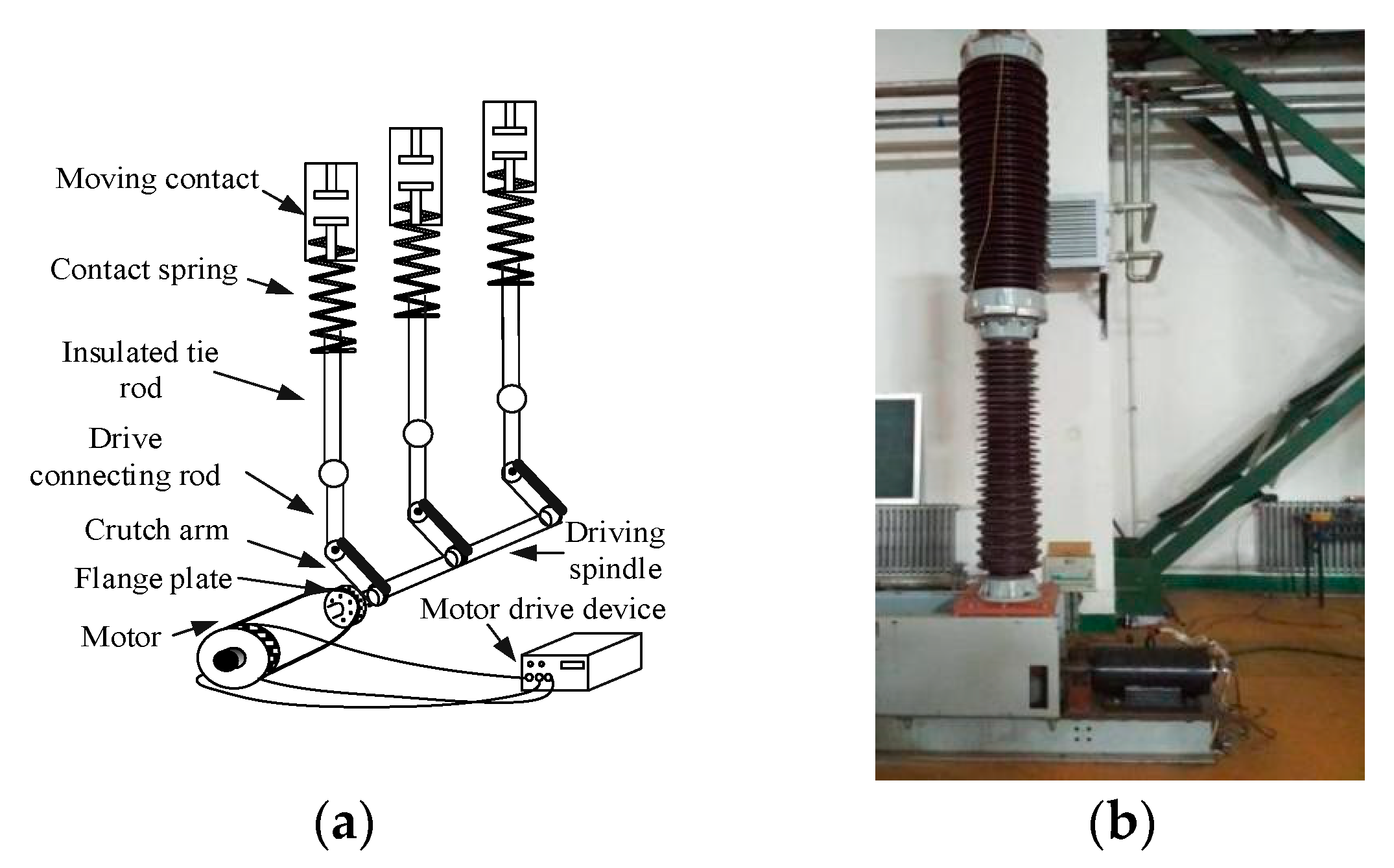
Figure 1.
Motor operating mechanism structure. (a) Structure diagram; (b) Physical diagram.
Figure 1.
Motor operating mechanism structure. (a) Structure diagram; (b) Physical diagram.
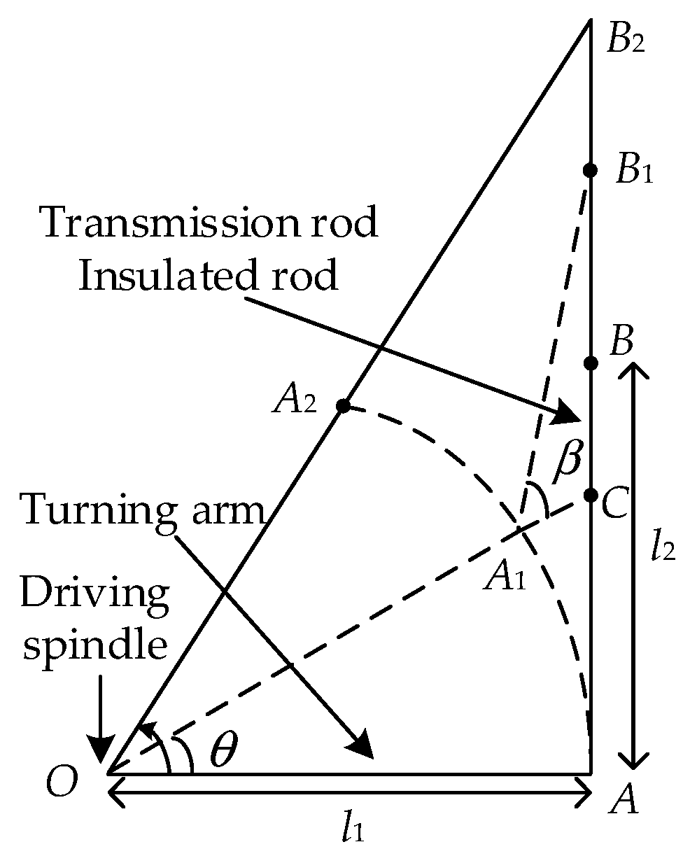
Figure 2.
Motion process of transmission mechanism.
Figure 2.
Motion process of transmission mechanism.
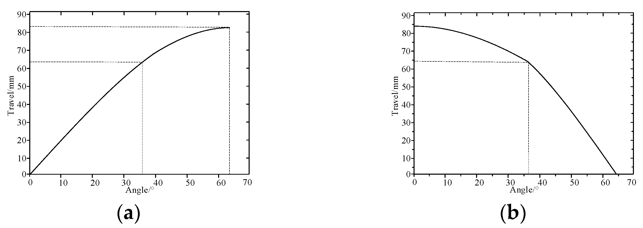
Figure 3.
The relationship between the rotation angle of the motor and the linear displacement of the insulation rod. (a) Closing stage; (b) Opening stage.
Figure 3.
The relationship between the rotation angle of the motor and the linear displacement of the insulation rod. (a) Closing stage; (b) Opening stage.
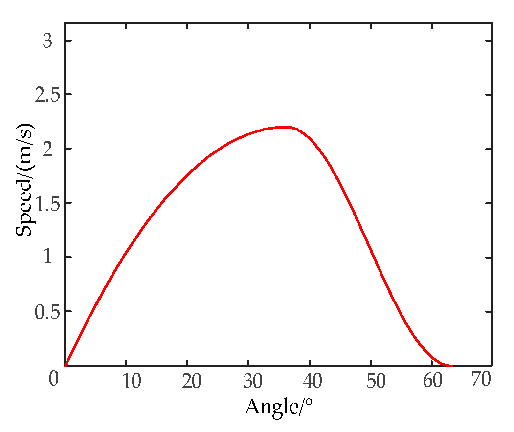
Figure 4.
Conversion curve of motor rotation angle and moving contact speed.
Figure 4.
Conversion curve of motor rotation angle and moving contact speed.
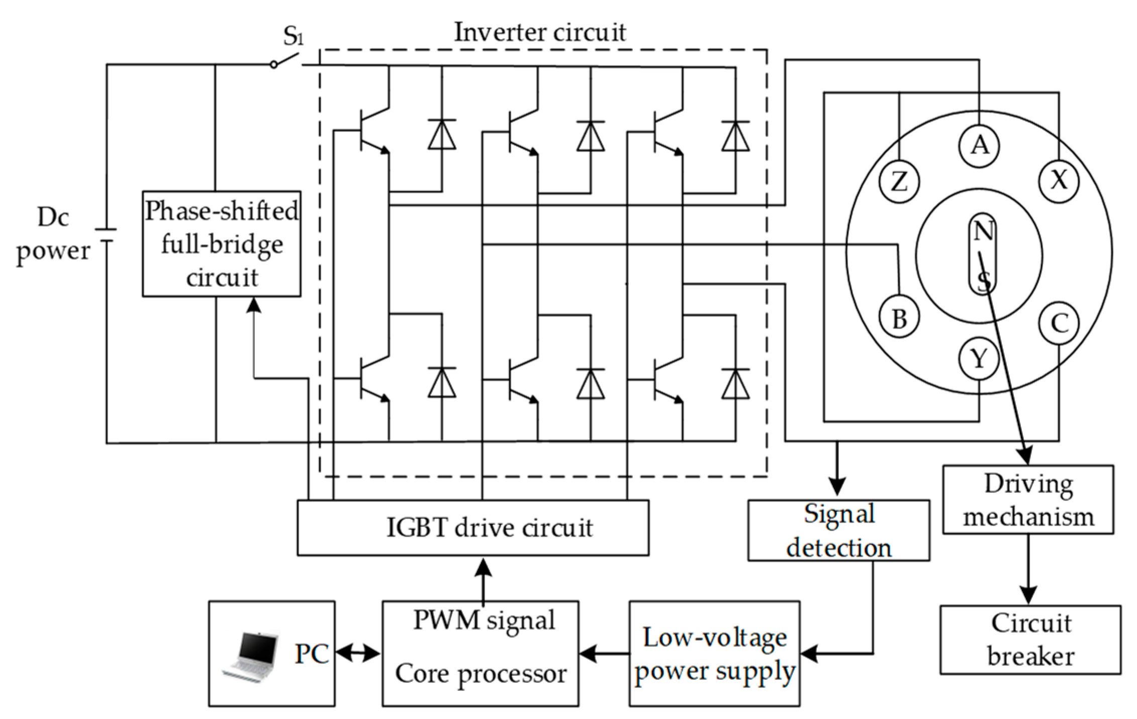
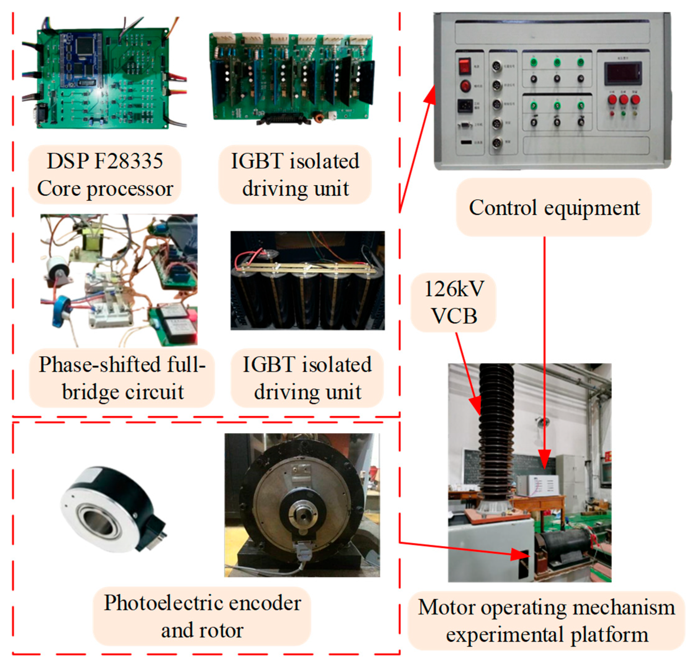
Figure 5.
Motor drive control device.
Figure 5.
Motor drive control device.
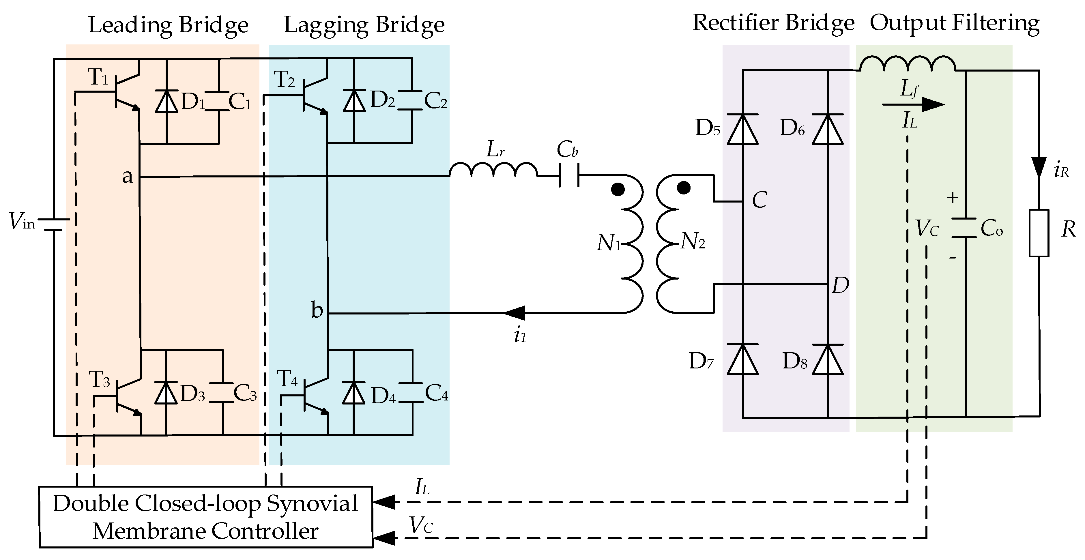
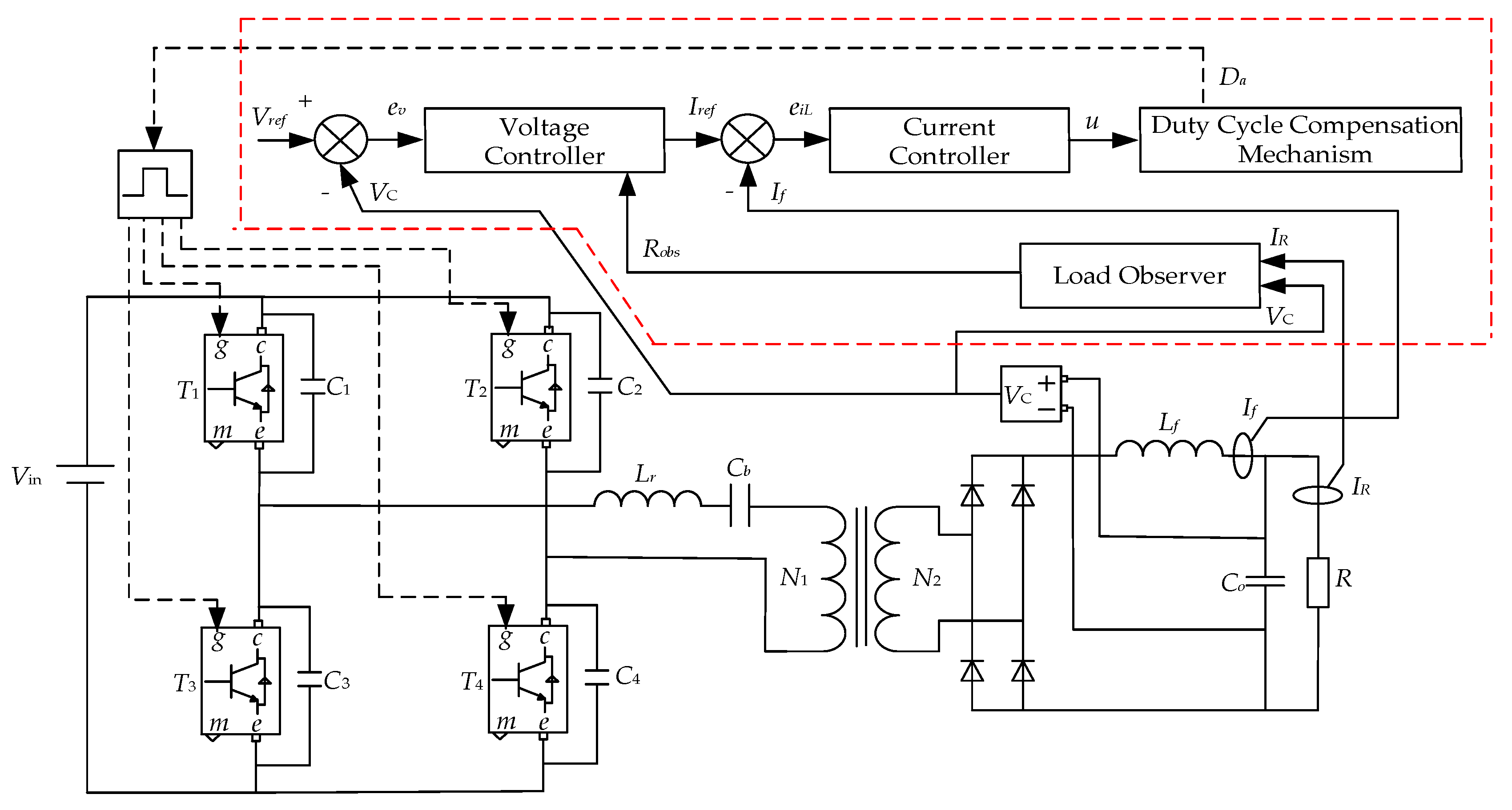
Figure 6.
Phase-shifted full-bridge circuit topology.
Figure 6.
Phase-shifted full-bridge circuit topology.
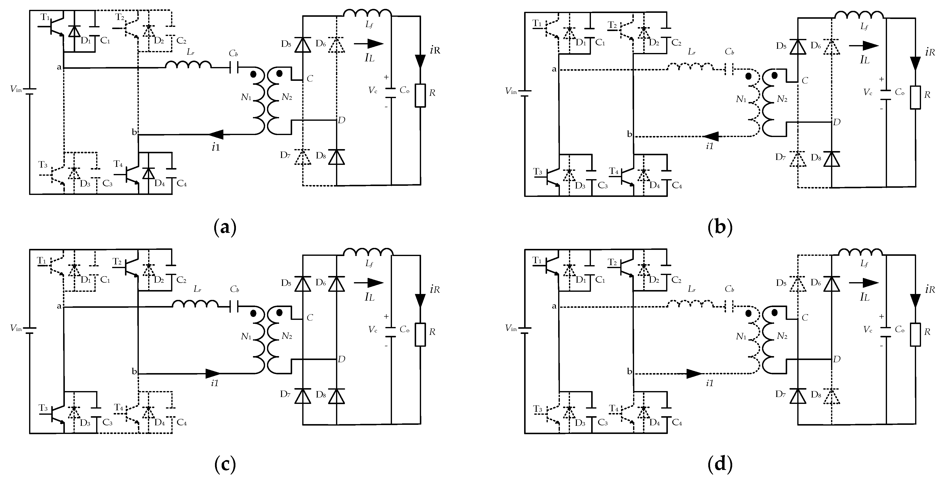
Figure 7.
Working state of phase-shifted full-bridge circuit. (a) T1, T4 are on. (b) T3, T4 are on. (c) T2, T3 are on. (d) T1, T2 are on.
Figure 7.
Working state of phase-shifted full-bridge circuit. (a) T1, T4 are on. (b) T3, T4 are on. (c) T2, T3 are on. (d) T1, T2 are on.
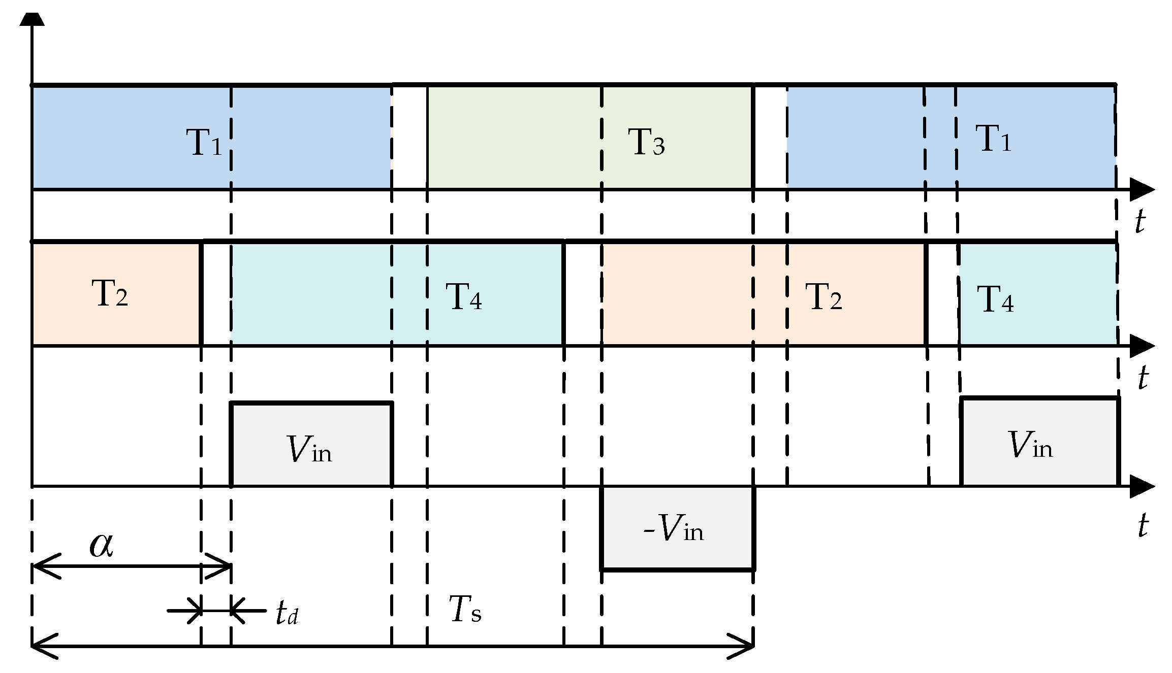
Figure 8.
The working state waveform of the converter.
Figure 8.
The working state waveform of the converter.
Figure 9.
Circuit equivalent model.
Figure 9.
Circuit equivalent model.
Figure 10.
Simplified mathematical model of voltage outer loop terminal sliding mode controller.
Figure 10.
Simplified mathematical model of voltage outer loop terminal sliding mode controller.
Figure 11.
Simplified mathematical model of current inner loop linear sliding mode controller.
Figure 11.
Simplified mathematical model of current inner loop linear sliding mode controller.
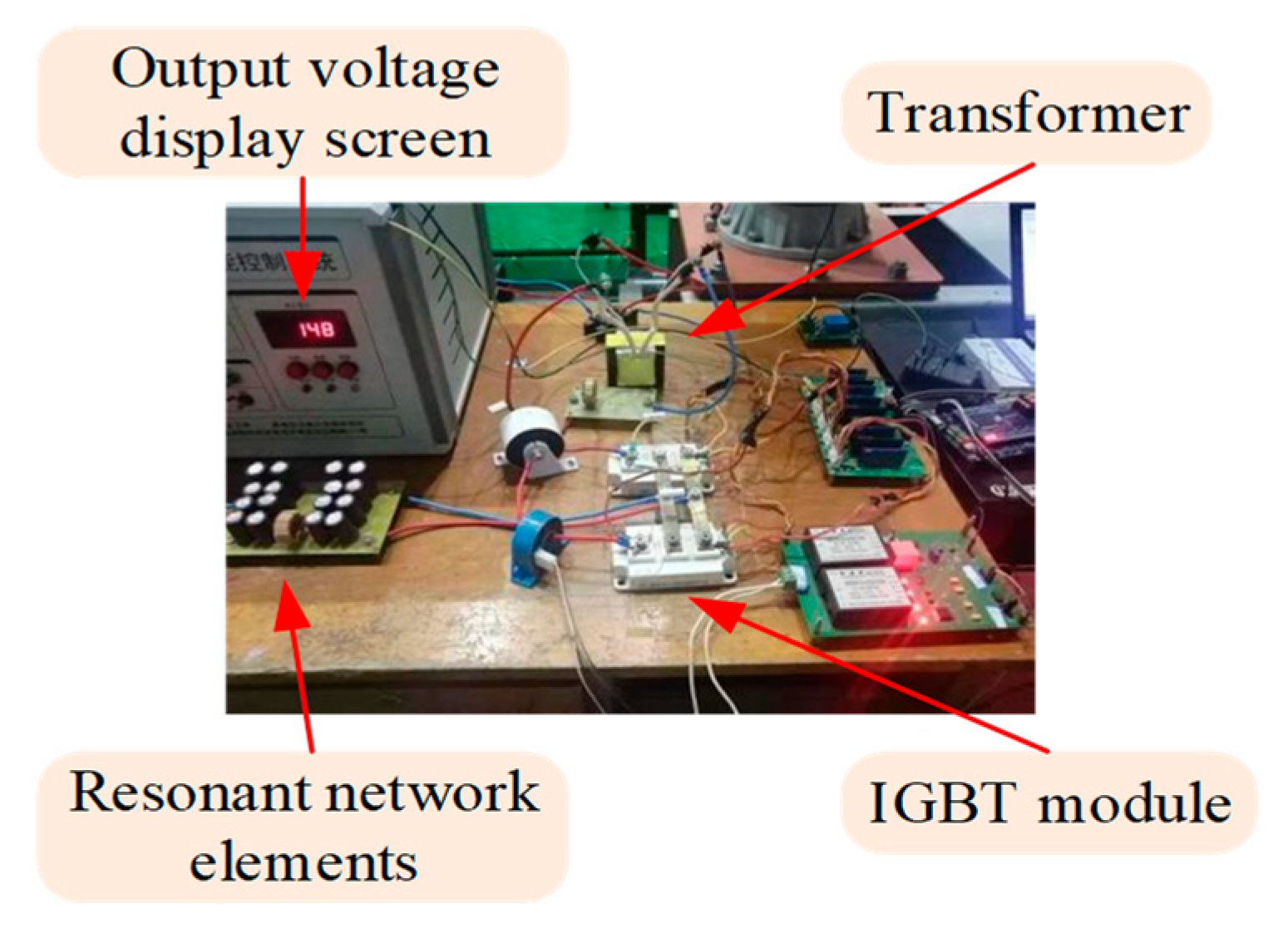
Figure 12.
Test platform.
Figure 12.
Test platform.
Figure 13.
Boost experimental results of phase-shifted full-bridge converter.
Figure 13.
Boost experimental results of phase-shifted full-bridge converter.
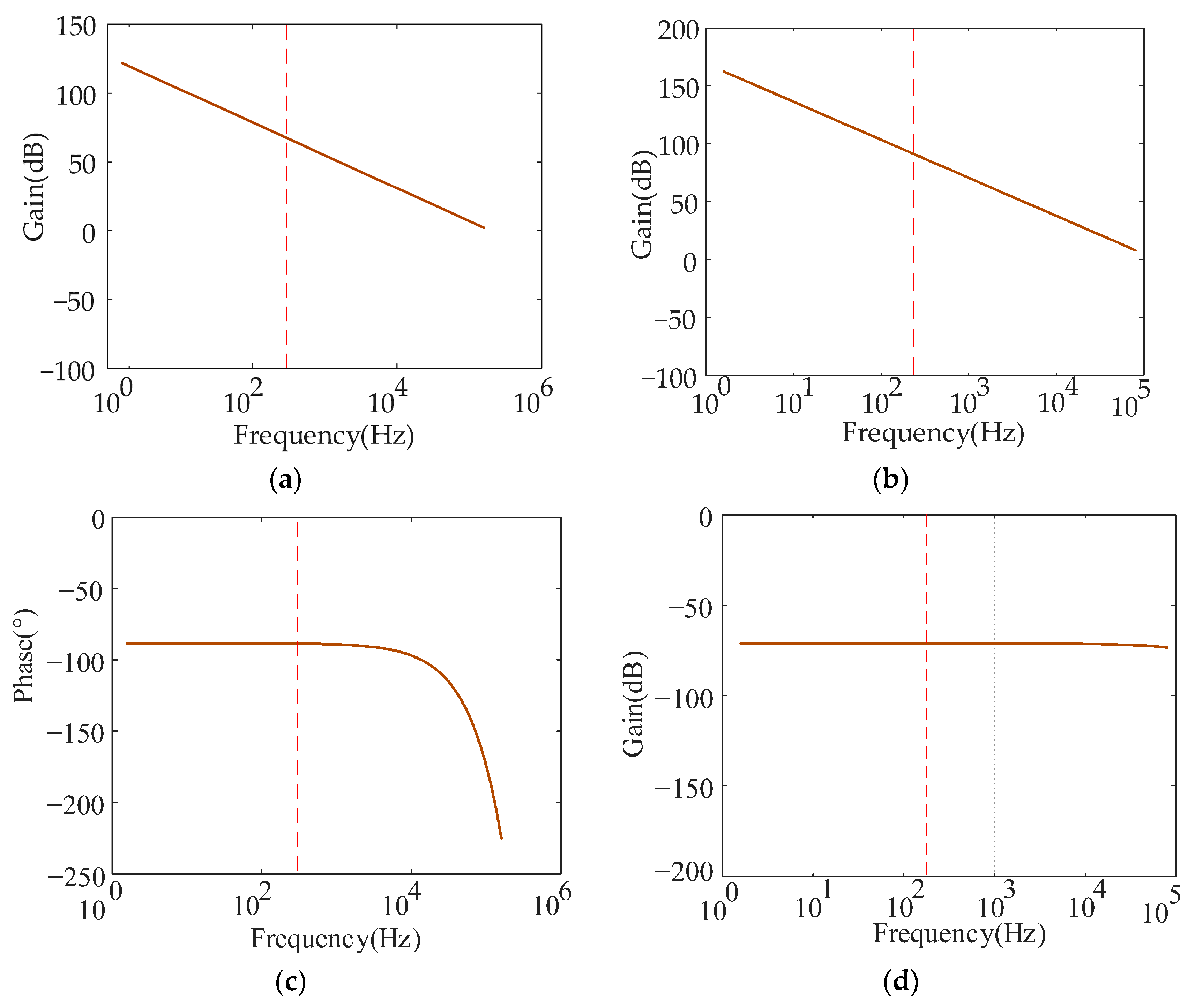
Figure 14.
Bode diagram of double closed-loop sliding mode control system (Vin = 200 V, fs = 20 kHz). (a) Amplitude-frequency characteristics of current loop (unit: dB/Hz); (b) Amplitude-frequency characteristics of voltage loop (unit: dB/Hz); (c) Phase-frequency characteristics of current loop (unit: deg/Hz); (d) Phase-frequency characteristics of voltage loop (unit: deg/Hz).
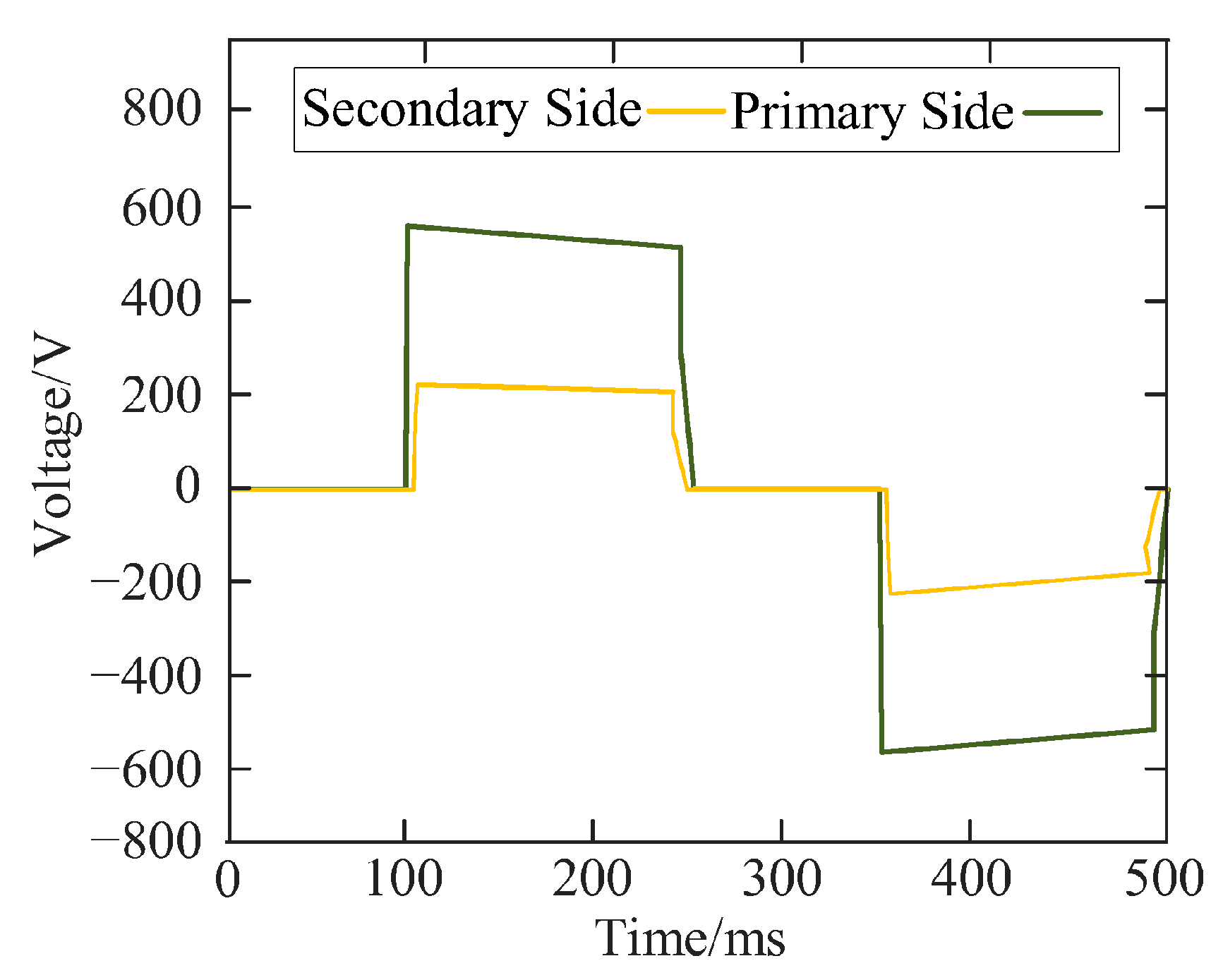
Figure 15.
The primary and secondary side voltage of the converter.
Figure 15.
The primary and secondary side voltage of the converter.
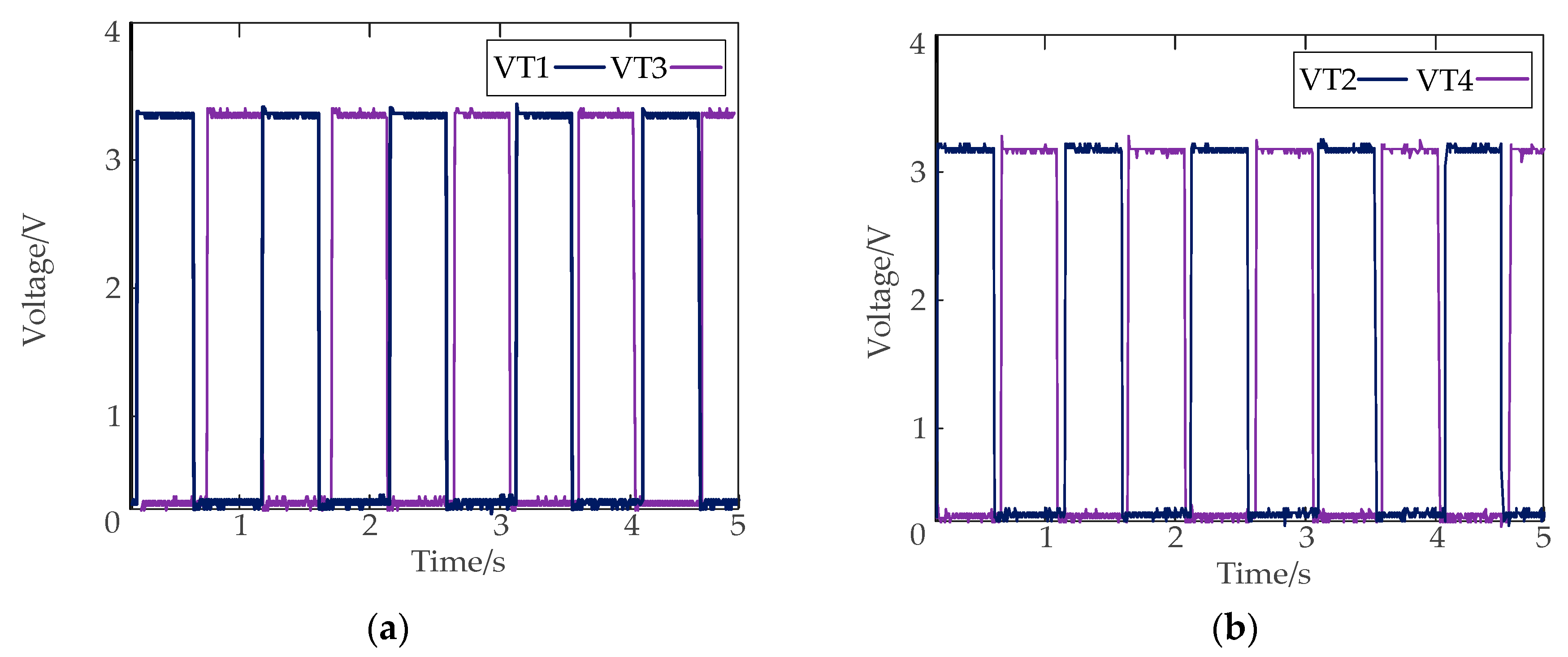
Figure 16.
Power tube drive signal waveform. (a) T1 and T3; (b) T2 and T4.
Figure 16.
Power tube drive signal waveform. (a) T1 and T3; (b) T2 and T4.
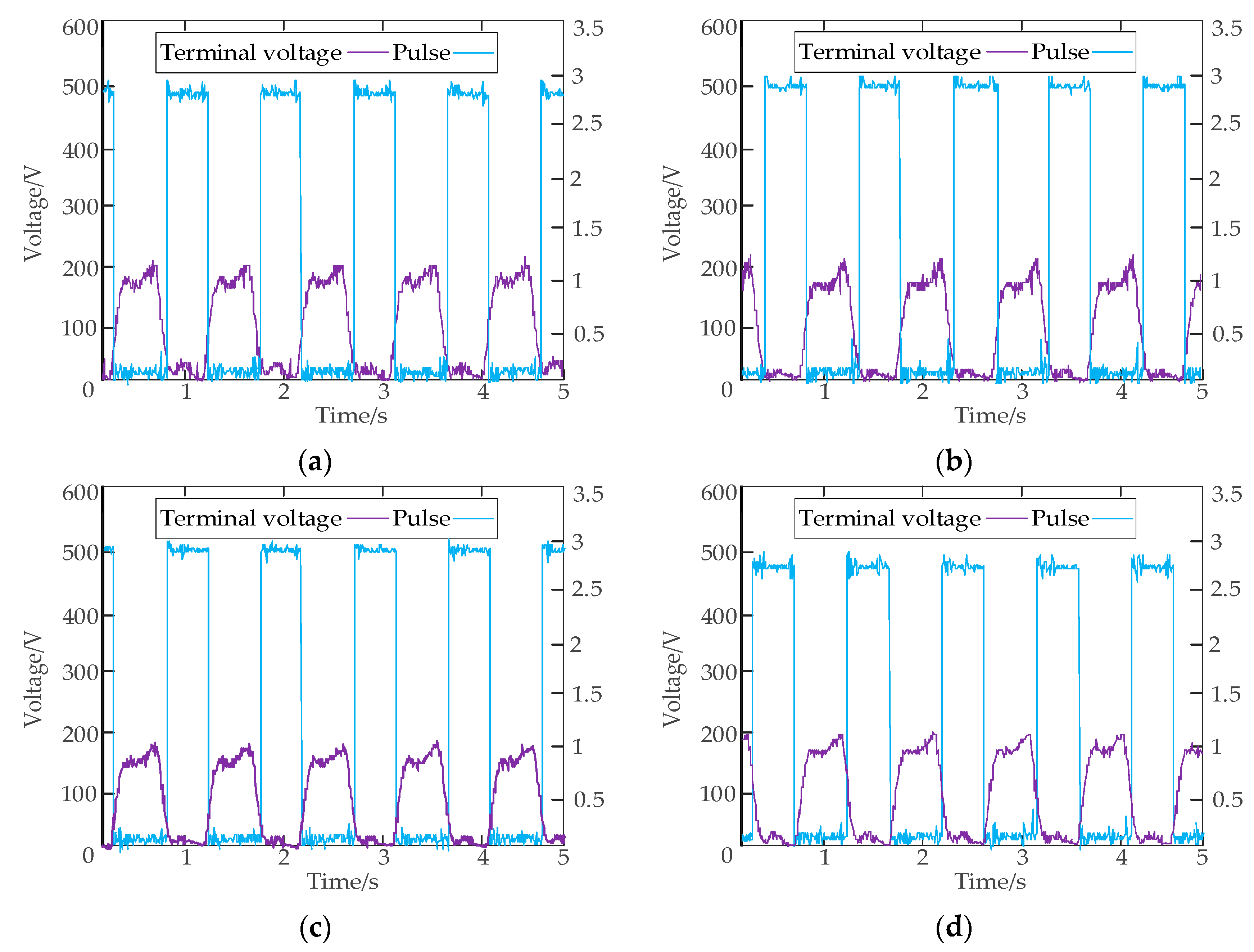
Figure 17.
ZVS implementation effect verification waveform (Vin = 200 V, fs = 20 kHz). (a) Lead bridge arm upper tube T1 drive signal and terminal voltage; (b) Lead bridge arm lower tube T3 drive signal and terminal voltage; (c) Lag bridge arm upper tube T2 drive signal and terminal voltage. (d) Lag bridge arm lower tube T4 drive signal and terminal voltage.
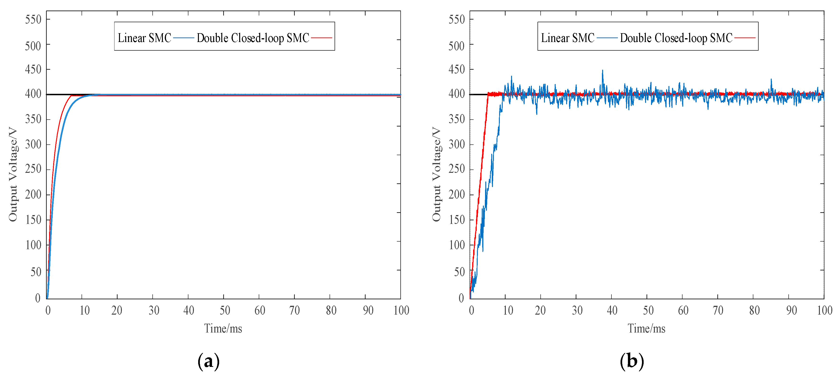
Figure 18.
Output voltage dynamic response of converter linear SMC and double closed-loop SMC. (a) Simulation results; (b) Experimental results.
Figure 18.
Output voltage dynamic response of converter linear SMC and double closed-loop SMC. (a) Simulation results; (b) Experimental results.
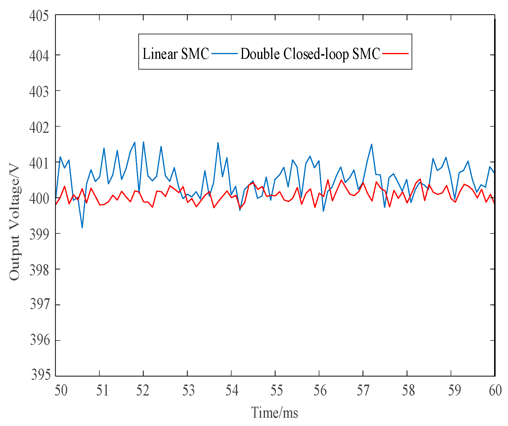
Figure 19.
Comparison of the output voltage ripple of the converter in the steady-state phase (t = 50–60 ms).
Figure 19.
Comparison of the output voltage ripple of the converter in the steady-state phase (t = 50–60 ms).
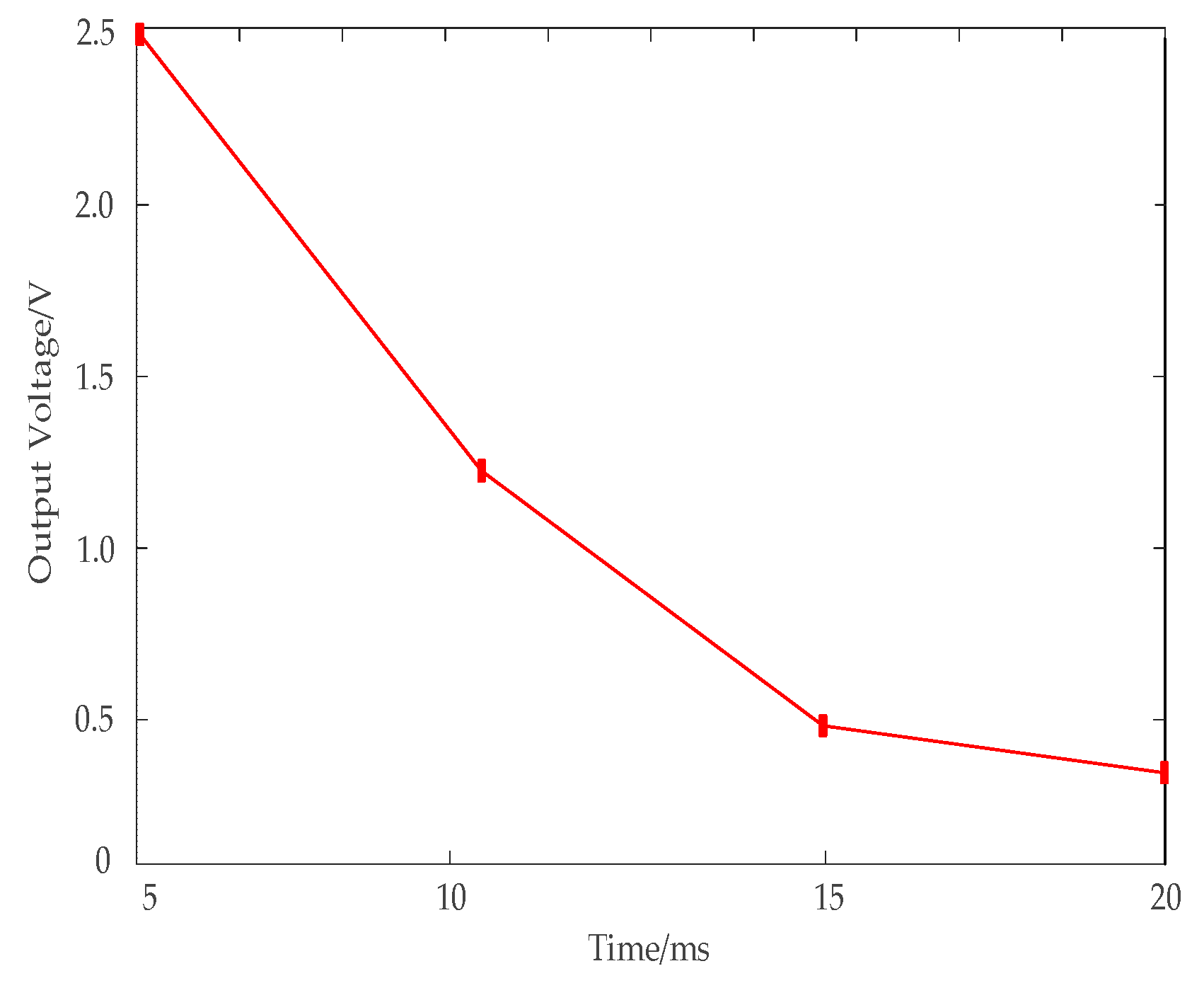
Figure 20.
The relationship between output voltage ripple peak and switching frequency.
Figure 20.
The relationship between output voltage ripple peak and switching frequency.
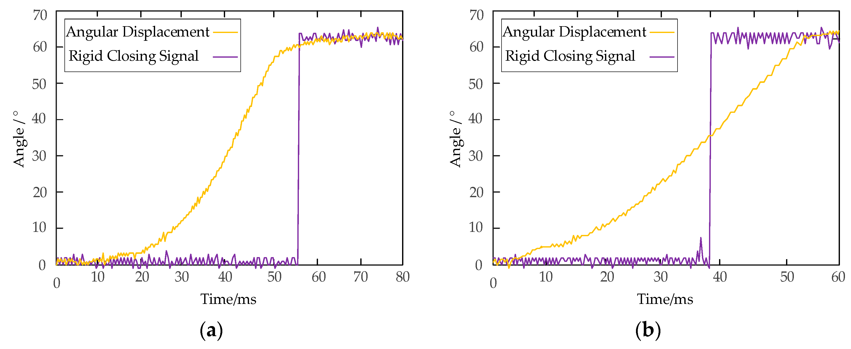
Figure 21.
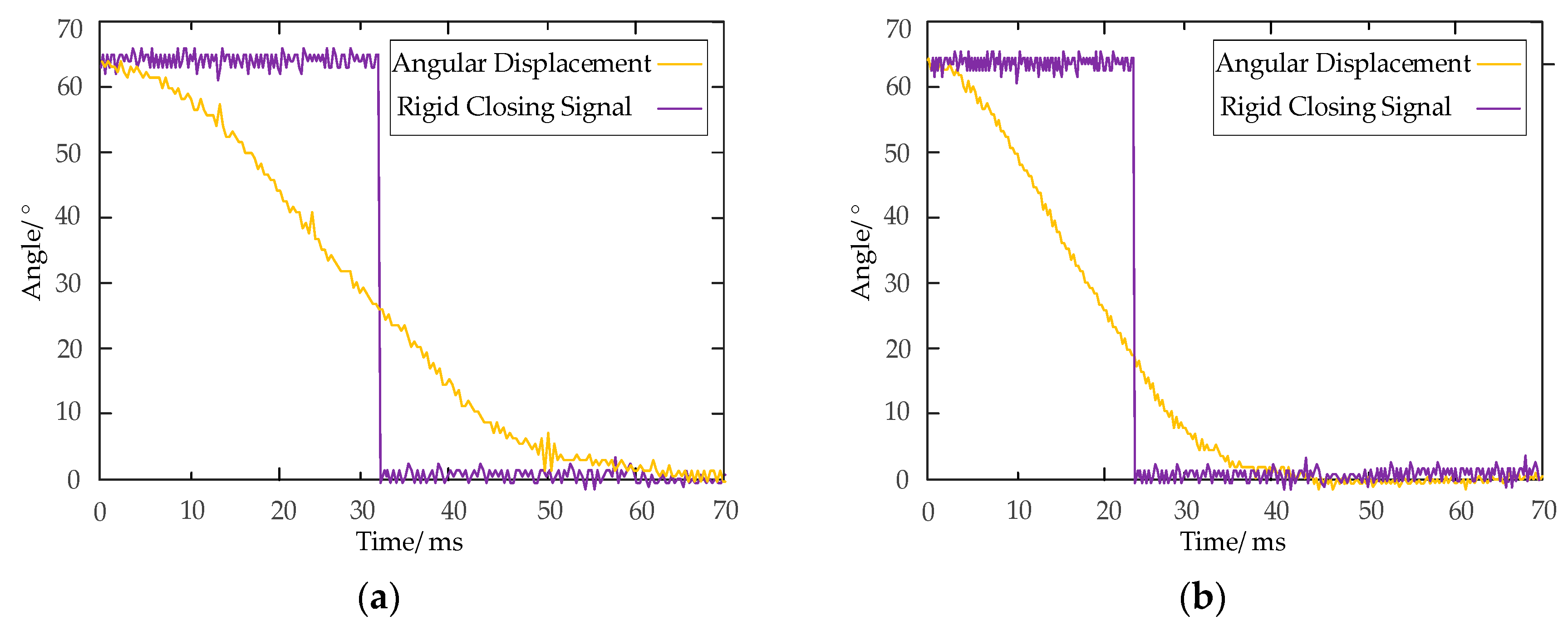
Closing test results. (a) Scheme 1; (b) Scheme 2.
Figure 21.
Closing test results. (a) Scheme 1; (b) Scheme 2.
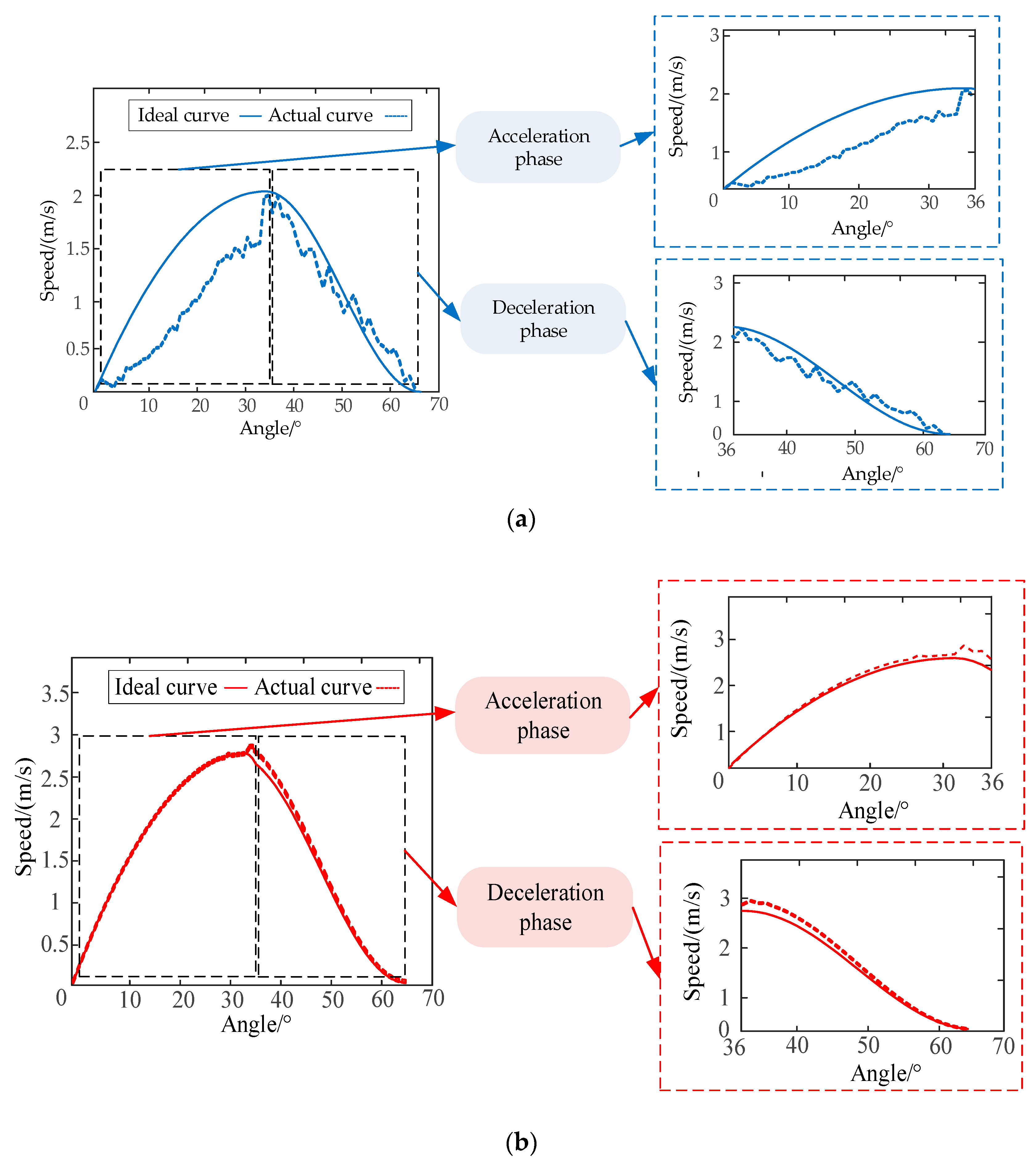
Figure 22.
The actual action speed curve of moving contact. (a) Scheme 1; (b) Scheme 2.
Figure 22.
The actual action speed curve of moving contact. (a) Scheme 1; (b) Scheme 2.
Figure 23.
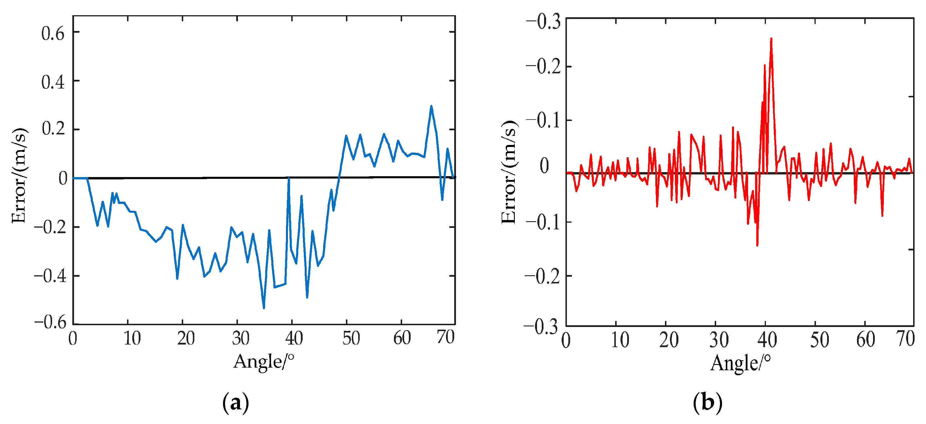
Velocity tracking error curve. (a) Scheme 1; (b) Scheme 2.
Figure 23.
Velocity tracking error curve. (a) Scheme 1; (b) Scheme 2.
Figure 24.
Opening test results. (a) Scheme 1; (b) Scheme 2.
Figure 24.
Opening test results. (a) Scheme 1; (b) Scheme 2.
Table 1.
Comparison of converter topology performance.
Table 1.
Comparison of converter topology performance.
| Topological Type | Insulation | Current Flow | Arc Extinction | Main Limitations |
|---|
| Forward-flyback converter | 1.2 kV | 50 A | 5 ms | Poor immunity |
| Hybrid half-bridge converter | 200 kV | 2 kA | 2 ms | Efficiency fluctuates greatly |
| Full-bridge converter | 100 kV | 3 kA | 3 ms | Circuit structure and control mechanism are complex |
| Multilevel converter | 80 kV | 5 kA | 1.5 ms | High cost |
| Boost converter integrates IGBT resistance-capacitance branch | 60 kV | 5.5 kA | 1 ms | Dynamic performance is susceptible to port voltage |
Table 2.
Characteristics of the control method.
Table 2.
Characteristics of the control method.
| Control Method | Response Speed/ms | Speed Error/% | Robustness | Main Limitations |
|---|
| PID | 28 | 4.5 | Feebleness | Poor immunity |
| NFTSMC | 18 | 2.8 | Middle | Serious chattering |
| MPC | 22 | 3.2 | Middle | Computation complexity |
Table 3.
The comparison results between the proposed method and the main control strategies.
Table 3.
The comparison results between the proposed method and the main control strategies.
| Performance Index | PID | MFPC | NFTSMC | Method of This Article |
|---|
| Stability (phase margin)/° | 42 | 58 | 72 | 76.8 |
| Speed error/% | 14.8 | 13.2 | 8.3 | 3.8 |
| Response time/ms | 3.2 | 25 | 18 | 4.8 |
| ZVS efficiency/% | 79 | 86 | 89 | 97.3 |
Table 4.
Requirements of opening and closing characteristics of 126 kV vacuum circuit breaker.
Table 4.
Requirements of opening and closing characteristics of 126 kV vacuum circuit breaker.
| Project | Unit | Reference Value |
|---|
| Contact opening distance | mm | 60 ± 2 |
| Contact over travel | mm | 24 ± 2 |
| Opening time | ms | 42 ± 2 |
| Average opening speed | m/s | 3.5 ± 0.2 |
| Average closing speed | m/s | 1.3 ± 0.2 |
| Closing time | ms | 70 ± 20 |
| Contact opening distance | mm | 60 ± 2 |
Table 5.
Length and mass of moving parts.
Table 5.
Length and mass of moving parts.
| Mass of Mechanism Parts | Quality (kg) | Length (mm) |
|---|
| Moving contact | 19.21 | / |
| Contact spring | 20.14 | / |
| Driving connecting rod | 1.37 | 140 |
| Insulating tie rod | 11.62 | 84 |
| Crutch arm | 3.36 | 109.2 |
Table 6.
Phase-shifted full-bridge circuit status.
Table 6.
Phase-shifted full-bridge circuit status.
| Working Condition | Function Specification |
|---|
| Power transmission phase | When one tube of the leading bridge arm and the other tube of the lagging bridge arm are simultaneously turned on (such as T1, T4 or T2, T3), the input voltage Vin is coupled to the secondary side N2 through the primary side N1 of the transformer, and then provides power to the load through the rectifier circuit. |
| Resonance transition stage | The power tube T1 and T2 are turned off, Cb and Lr form a resonance, so that the tube voltage drop of T2 is reduced to 0, the zero voltage conduction of T2 is realized, and the switching loss is reduced. |
| Continuation phase | When two tubes of the same side tubes of the two bridge arms are turned on (such as T1, T2 or T3, T4), that is, vab = 0, the rectifier circuit enters the freewheeling state, and the inductor current IL flows through the inductor Lf and the load R freewheeling. |
Table 7.
Design objectives of Lyapunov constraints and frequency domain.
Table 7.
Design objectives of Lyapunov constraints and frequency domain.
| Design Objective | Lyapunov Constraint | Spectral Domain Constrained |
|---|
| Astringency | ζ | ωi |
| Robustness | Δ | PM |
| Buffeting | Ki | GM |
Table 8.
Key parameters of voltage loop and current loop.
Table 8.
Key parameters of voltage loop and current loop.
| Parameter | Electric Current Loop | Voltage Control Loop |
|---|
| Crossover frequency | | |
| Phase margin | | |
Table 9.
Simulation circuit parameters.
Table 9.
Simulation circuit parameters.
| Parameter Name | Sign | Numerical Value | Unit |
|---|
| Input voltage | Vin | 200 | V |
| Switching frequency | fs | 20 | kHz |
| Ratio of transformer | n | 1/3 | / |
| Primary side inductance | Lr | 8 | uH |
| Primary side capacitance | Cb | 0.05 | uF |
| Filter inductance | Lf | 2.3 | uH |
| Smoothing capacitance | Co | 2200 | uF |
| Load | R | 50 | Ω |
| Parallel absorption capacitor | C1–C4 | 0.01 | uF |
| Duty cycle of power switch | d | 0.5 | / |
| Phasing angle | α | 10 | % |
| Dead time | td | 3.3 | us |
| IGBT thermal resistance | Rds | 0.12 | K/W |
Table 10.
Experimental data of output voltage ripple peak at different switching frequencies.
Table 10.
Experimental data of output voltage ripple peak at different switching frequencies.
| Switching Frequency (kHz) | Peak Voltage Fluctuation ΔV (V) |
|---|
| 5 | 2.5 |
| 10 | 1.2 |
| 15 | 0.44 |
| 20 | 0.3 |
Table 11.
Main data of closing tes.
Table 11.
Main data of closing tes.
| Experimental Parameters | Scheme 1 | Scheme 2 |
|---|
| Closing time/ms | 73.6 | 52.1 |
| Rigid closing time/ms | 53.8 | 39.2 |
| Starting delay time/ms | 11.1 | 4.8 |
Table 12.
Main technical parameter data of opening test.
Table 12.
Main technical parameter data of opening test.
| Experimental Parameters | Scheme 1 | Scheme 2 |
|---|
| Total gate time/ms | 64.2 | 45.7 |
| Rigid opening time/ms | 31.1 | 22.3 |
| Maximum opening speed/(m/s) | 2.63 | 3.31 |
Table 13.
Comparison of dynamic response indicators.
Table 13.
Comparison of dynamic response indicators.
| Performance Index | Specific Numerical Changes | Increase (%) |
|---|
| Closing time | 73.6 → 52.1 ms | −29.2 |
| Opening time | 73.6 → 52.1 ms | +31.7 |
| Maximum Closing speed | 2.24 → 2.95 m/s | −28.8 |
| Maximum opening speed | 2.63 → 3.31 m/s | +25.9 |
