Article

Grid-Forming Buck-Type Current-Source Inverter Using Hybrid Model-Predictive Control

School of Engineering and Computer Science, PEMD Group, Washington State University Vancouver, Vancouver, WA 98686, USA
*
Author to whom correspondence should be addressed.
Energies 2025, 18(15), 4124; https://doi.org/10.3390/en18154124
Submission received: 29 May 2025 / Revised: 29 July 2025 / Accepted: 31 July 2025 / Published: 4 August 2025
(This article belongs to the Section F3: Power Electronics)

Abstract

Grid-forming (GFM) inverters have recently seen wider adoption in microgrids and inverter-based-resource (IBR)-penetrated grids, and are primarily used to establish grid voltage under a wide array of conditions. In the existing literature, GFM control is almost exclusively applied using voltage-source inverters (VSIs). However, due to the inherent limitations of available semiconductor devices’ current ratings, inverter-side current must be limited in VSIs, particularly during grid-fault conditions. These limitations complicate the real-world application of GFM functionality in VSIs, and complex control methodologies and tuning parameters are required as a result. In the following study, GFM control is instead applied to a buck-type current-source inverter (CSI) using a combination of linear droop-control and finite-control-set (FCS) mode-predictive control (MPC) that will be referred to herein as hybrid model-predictive control (HMPC). The resulting inverter features a simple topology, inherent current limiting capabilities, and a relatively simple and intuitive control structure. Verification was performed on a 1MVA/630V system via MATLAB/Simulink, and the simulation results demonstrate strong performance in voltage establishment, power regulation, and low-voltage ride through under-grid-fault conditions, highlighting its potential as a competent alternative to VSIs in GFM applications, and lacking the inherent limitations and/or complexity of existing GFM control methodologies.

1. Introduction

Grid-forming (GFM) power inverters are key components of microgrid systems and play an integral role in the effective use of inverter-based resources (IBRs) within larger electrical grids, due to their capacity to both generate and maintain grid voltage. As a result, GFM technology has been identified as a critical facet of the ongoing renewable energy integration [1], particularly in geographic areas where IBRs meet a significant percentage of local demand for power [2]. Looking to the future, GFM technology has the potential to ease the increased implementation of low- or even zero-inertia power sources, such as photovoltaics (PV) and wind [3], and stabilize existing low-inertia systems [4]. In terms of overall grid stability, both grid-following (GFL) and GFM inverters have been shown to improve the stability of power grids with any level of IBR penetration [5]. GFM technology naturally lends itself to the implementation of AC microgrid systems [6], which continue to see further research and wider adoption globally.
The operation of a GFM inverter, along with a number of common control methodologies, applications, and challenges is outlined in detail in [7,8], so we will provide a brief summary in here as a regular research article. GFM inverters, as opposed to GFL inverters, are inverters that function as stand-alone AC voltage and grid frequency regulators; that is, they may operate independent of the larger grid in the case of “islanded mode,” or synchronize with the larger grid in the case of “grid-connected” mode. Most importantly, GFM inverters can accomplish this without the use of a phase-locked loop (PLL), allowing the inverter to adapt quickly and independently to changes in grid conditions, and potentially preventing catastrophic degradations in grid stability.
A number of control methodologies exist and are in active use for the control of GFM inverters, and an exhaustive list of these methodologies along with their advantages and disadvantages may be found in [7]. The most common approaches in state-of-the-art GFM inverters include droop control, virtual synchronous generator (VSG) control, and virtual oscillator control (VOC). Though a detailed analysis of each methodology’s approach, advantages, and disadvantages is beyond the scope of this paper, a brief discussion of the relevant points follows, along with a summary and comparison of each methodology, available in Table 1.
Frequency-based and angle-based droop control is the simplest and most common approach to the control of GFM inverters. However, due to the linear nature of droop control, when unexpected events such as line-ground faults occur, the control algorithm may react unexpectedly, resulting in shutdown or damage to the inverter itself [9]. VSG control is a common alternative to droop control that seeks to minimize the effects of high IBR penetration and its corresponding lack of physical inertia when compared to a traditional, generator-based grid; however, the implementation of such systems (though sophisticated versions display high performance and fast responses) is algorithmically complex and requires the use of multiple cascaded control stages [10]. VOC, for its part, seeks to virtually emulate the operation of a non-linear oscillator, but provides no inherent overcurrent protection. Dispatchable virtual oscillator control (dVOC) shows some promising results in correcting this disadvantage of VOC, but research is ongoing, and current implementations remain very complex and are not yet ready to be implemented under real-world conditions [8]. The above summary leads us the conclusion that, despite available control methodologies for the operation of GFM inverters, there continues to exist a need for a simple, easily implemented inverter topology and corresponding control methodology that meets basic criteria for real-world operation, demonstrates current-limiting behavior, and does not depend on the implementation of a PLL, allowing it to function in islanded or grid-connected modes. Such a GFM inverter should display reasonably good performance in steady-state conditions, respond quickly to transient changes in real and reactive power demands, and demonstrate the capacity for fault-ride-through scenarios.
On the other hand, the type of GFM inverters may be divided into two major categories: voltage-source inverters (VSIs) and current-source inverters (CSIs) [8]. The use of VSI, though simple in its topology and implementation, lacks built-in current-limiting control. This complicates the control side of the equation, and additional layers of often complex current-limiting control algorithms are required to make a voltage-source GFM inverter feasible in real-world applications. In contrast, CSIs dispense with this disadvantage of VSIs, featuring inherent current-limiting capabilities that can be implemented using little-to-no additional control mechanisms [11], therefore reducing their final cost and complexity. Unfortunately, very little attention has been paid to the study on the CSI-based GFM method. Therefore, we further expend the scope of GFM control based on a CSI [12], which demonstrates the required inherent current-limiting capabilities as well as grid-friendly voltage waveforms [11]. CSIs have already shown themselves to be useful and have been adopted in applications as widespread as medium-voltage (MV) electric motor drives [13] and offshore wind energy conversion [14], and have enormous potential in high-power, low-voltage applications. In addition, we propose the use of a finite-control-set (FCS) model-predictive control (MPC) [15] approach for the control of the aforementioned CSI, due to its simple structure and ease of implementation. FCS-MPC works by optimizing control inputs as a function of its own predictions regarding the evolution of state variables, and has already been applied extensively to the regulation of grid-following inverters [16]. Despite this, the use of CSIs in GFM control contexts is all but missing from both academic literature and industry applications. The single existing study on the use of CSIs in GFM control utilizes a linear droop-control approach and depends on an ideal DC current source [11], which is difficult to generate in real-world conditions.
In this study, we propose that the CSI in this case be preceded by a voltage-to-current regulation stage, implemented using a buck converter, which is turn-controlled using a simple, linear droop-control methodology. This dispenses with the difficulty of an ideal DC current source, while maintaining a relatively simple control methodology to meet practical requirements in real-world applications. The resulting control algorithm, due to the necessity of controlling both the buck converter and CSI, is referred to herein as hybrid model-predictive control (HMPC). Specifically, FCS-MPC is applied for the single-bridge CSI to attain superb dynamic responses and limit the switching frequency. And continuous-control-set (CCS) MPC is used to regulate the buck stage to maintain the switching frequency at a fixed value and smooth the DC current. The result meets the requirements set out above, maintaining acceptable performance under steady-state conditions: a reasonable degree of current-limiting behavior, fault-ride-through capability, and a lack of dependence on a PLL for its operation.
Our key contributions can be categorized into three folds. First, we further extend the scope of the type of GFM inverters by presenting the GFM based on the unique buck-type CSI. Second, it is the first time to realize CSI-based GFM using the MPC approach, which further extends the horizon of study on the MPC-based GFM method. Last but not least, the developed HMPC is a unique and intuitive method which can potentially be further applied to broader GFM inverters.
We begin with a detailed explanation of the inverter’s topology and components, followed by a breakdown of the relevant mathematical models in Section 2. This is followed by a detailed presentation and analysis of the simulated inverter’s performance under a variety of conditions, and finally a comparison to a linear droop-control approach in Section 3. In Section 4, some discussion is conducted, and final conclusions are drawn.

2. Materials and Methods

2.1. Buck-Type CSI

The schematic diagram of a buck-type CSI can be seen in Figure 1.
As shown, a DC voltage source is connected through a buck converter to a CSI. The capacitor bank C i is installed at the CSI’s AC outputs and connected to the grid via an isolation transformer. R s and L s represent grid-equivalent resistance and inductance. By converting three-phase quantities into space-vector form in αβ coordinates, the dynamic model of the CSI’s AC side is given by the following:
C i d v C i d t = i w i i g
where v C i is the space vector of the capacitor voltage, as well as the voltage at the transformer’s primary side. i w i and i g are space vectors of the PWM current output from the CSI and the grid current, respectively [17]. i w i is confined to 6 active-state vectors and one zero-state vector, which can be generated by 9 available switching states, including 6 active switching states and 3 redundant zero-switching states [18]. (1) may be discretized as follows:
v C i p k + 1 = v C i k + T s C i i w i k i g k ,
where k is the sequence number of the sampling instant and T s is the sampling interval [17]. Thereafter, the capacitor voltage at the future sampling instant v C i p ( k + 1 ) can be predicted.
At the DC side, the dynamics of the inductor current i d c is given by the following:
L d c d i d c d t = v A v d c i
where L d c is the DC choke’s inductance, v d c i is the CSI’s DC-side voltage, and v A is the switched voltage inside the buck converter [17]. (3) can be further discretized as follows:
i d c p k + 1 = i d c k + D T s L d c V d c v d c i k + 1 D T s L d c = i d c k T s L d c v d c i k + T s V d c L d c D ,
where D is the duty ratio of S d c . Using (4), the DC current at the future sampling instant can be predicted and regulated by varying the duty ratio.

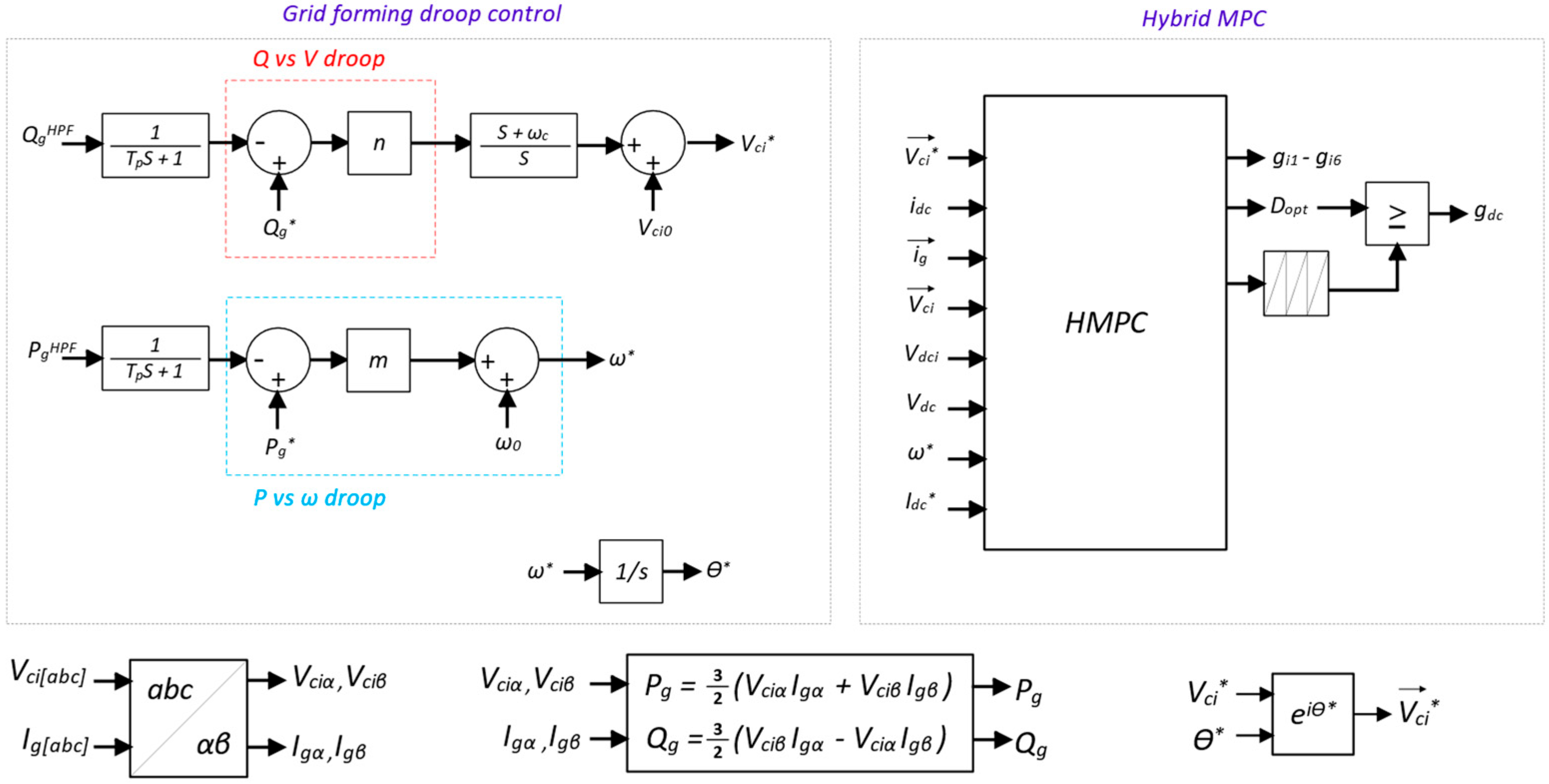
2.2. Grid-Forming Functionality

The relevant droop equations are given by the following:
ω = ω 0 + m P g P g H P F V C i = V C i 0 + n Q g Q g H P F s + ω c s ,
where P g and Q g are reference real and reactive power, respectively [7]. ω and ω 0 are reference and nominal angular frequency, respectively. V C i and V C i 0 are the reference and nominal capacitor voltage magnitude, respectively. P g H P F and Q g H P F are high-pass-filtered instantaneous real and reactive power, respectively. ω c is the cutoff frequency of the proportional-integral stage. m and n denote real power-frequency droop gain and reactive power-voltage droop gain.
Real power-frequency droop gain m is calculated using the following:
m = Δ f m a x Δ P m a x ,
where Δ p m a x   and Δ P m a x represent the maximum allowable deviation in nominal frequency and maximum allowable variation in power, respectively, while reactive power-voltage droop gain n is calculated using the following:
n = Δ V m a x Δ Q m a x ,
where Δ V m a x   and Δ Q m a x represent the maximum allowable deviation in nominal voltage and maximum allowable variation in reactive power, respectively.
The reference voltage angle, θ , can be obtained from the integral of ω ; thereafter, the reference capacitor voltage vector is given by the following:
v C i = V C i e j θ .
The droop-control approach shown in Figure 2 is the basis for the device’s grid-forming functionality.

2.3. Hybrid Model-Predictive Control
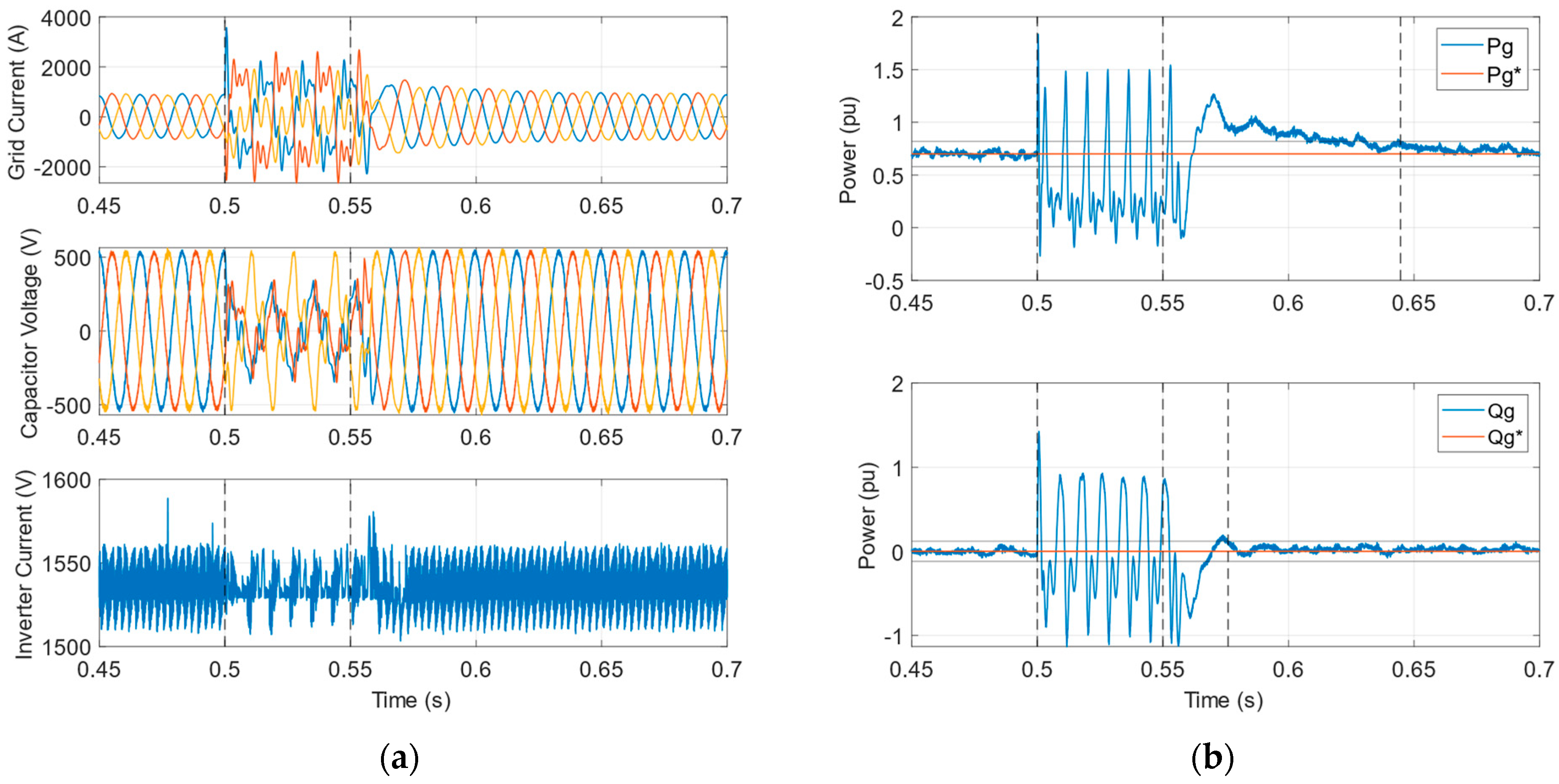
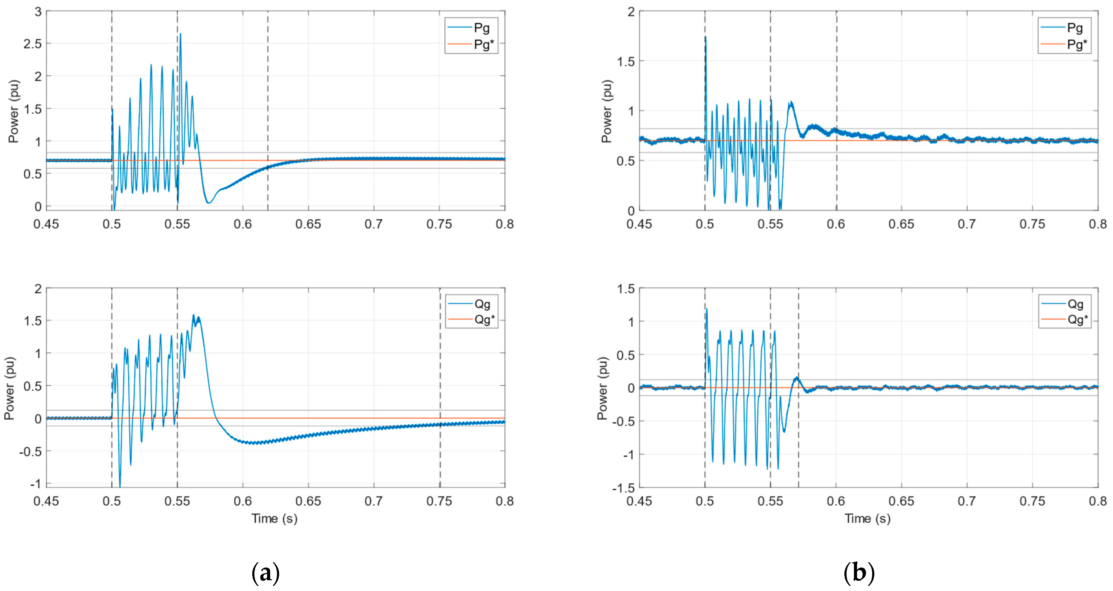
HMPC consists of FCS-MPC to regulate the capacitor voltages and CCS-MPC to control DC current. An optimal switching state is selected during each sampling interval. To limit the number of switching commutations for the purpose of switching loss reduction, a maximum of one switching commutation, including one turn-on and one turn-off action, is allowed for the newly selected switching state of the CSI. The cost function (sometimes referred to as the objective function) used for evaluating the switching states is given by the following:
g v k = v C i k + 1 v C i p k + 1 2 ,
where v C i ( k + 1 ) is the extrapolated reference and equal to v C i k · e j ω T s . CCS-MPC is applied to the buck stage by comparing the duty ratio with a sawtooth carrier wave. The derivative of the cost function as follows,
  g i k = i d c i d c p k + 1 2 d g i d D = 0 ,
provides the optimal duty ratio. Substituting (4) into (8), the duty ratio resulting in a derivative of 0 is given by the following:
D 0 k = L d c V d c T s i d c i d c k + T s L d c v d c i k .
The final applied optimal duty ratio is given by the following:
D o p t = 1 i f   D 0 > 1 D 0 i f   0 D 0 1 0 i f   D 0 < 0 .
The optimal duty ratio is then compared with a sawtooth carrier wave to generate the switching signal for S d c .
The HMPC logic described above is also summarized below, in the form of a flowchart, in Figure 3.

3. Results

The simulation was conducted on a 1MVA/630V buck-type CSI via MATLAB/Simulink R2021a, using the following parameters.

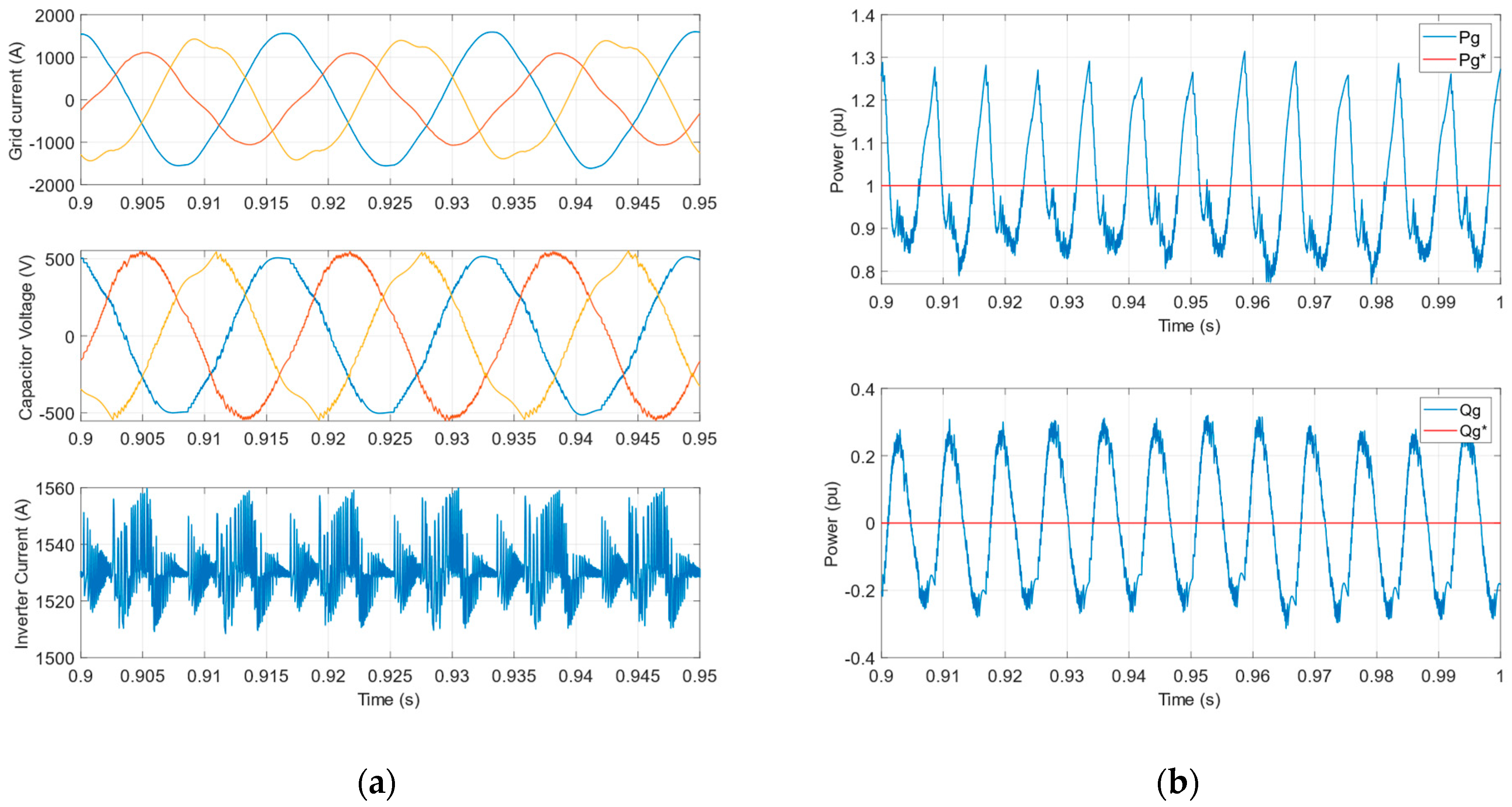
3.1. Steady-State Operation

Steady-state operation was evaluated under fixed reference real power P g and reactive power Q g of 1 pu and 0 pu, respectively. The relationship between R s and L s , under both strong and weak grid conditions, represents an X / R ratio of 10, unless otherwise noted. All subsequent results were collected over a 1 s period of steady-state operation. These parameters represent normal grid conditions for the purposes of this paper, and abnormal grid conditions will be presented relative to this benchmark.
The inverter’s steady-state operation was first simulated under the aforementioned normal grid conditions. Grid current i g , capacitor voltage C i , and DC current i d c waveforms are presented in Figure 4a, with all three remaining stable and periodic throughout steady-state operation. Grid current i g presents an average total harmonic distortion (THD) of 1.52% across its three phases, while capacitor voltage C i presents an average THD of 2.47% across its three phases.
Real power P g and reactive power Q g ’s waveforms, along with their respective references, are presented in Figure 4b, along with bounds of ±0.12 pu above and below their reference values, both indicated using a pair of dotted lines. Real power P g ’s maximum deviation from its reference value P g was ±0.11 pu, while reactive power Q g ’s maximum deviation from its reference value Q g was ±0.12 pu; that is, maximum real power P g reached 1.11 pu, while maximum reactive power Q g reached 0.12 pu, respectively, during steady-state operation.
Switching devices S1-6 operated with an average switching frequency F s w of 2489 Hz during steady-state operation.
The inverter’s steady-state operation was then simulated under unbalanced three-phase voltage conditions, in which the voltage at Phase A was reduced by a factor of 15%, with Phases B and C remaining at their set-point voltages. Grid current i g , capacitor voltage C i , and DC current i d c waveforms are presented in Figure 5a, with all three remaining stable and periodic, though slightly distorted, under unbalanced three-phase voltage conditions. Grid current i g presents an average total harmonic distortion (THD) of 7.01% across its three phases, while capacitor voltage C i presents an average THD of 5.37% across its three phases.
Real power P g and reactive power Q g ’s waveforms, along with their respective references, are presented in Figure 5b. Real power P g ’s maximum deviation from its reference value P g was ±0.34 pu, while reactive power Q g ’s maximum deviation from its reference value Q g was ±0.35 pu; that is, maximum real power P g reached 1.34 pu, while maximum reactive power Q g reached 0.35 pu, respectively, under unbalanced three-phase voltage conditions.
Switching devices S1-6 operated with an average switching frequency F s w of 2199 Hz under unbalanced three-phase voltage conditions.
The inverter’s steady-state operation was then simulated under an X / R ratio of 20, representing a 100% increase over the X / R ratio of normal grid conditions. Grid current i g , capacitor voltage C i , and DC current i d c waveforms are presented in Figure 6a, with all three remaining stable and periodic under an X / R ratio of 20. Grid current i g presents an average total harmonic distortion (THD) of 1.51% across its three phases, while capacitor voltage C i presents an average THD of 2.41% across its three phases.
Real power P g and reactive power Q g ’s waveforms, along with their respective references, are presented in Figure 6b. Real power P g ’s maximum deviation from its reference value P g was ±0.11 pu, while reactive power Q g ’s maximum deviation from its reference value Q g was ±0.10 pu; that is, maximum real power P g reached 1.11 pu, while minimum reactive power Q g reached −0.10 pu, respectively, under an X / R ratio of 20.
Switching devices S1-6 operated with an average switching frequency F s w of 2514 Hz under an X / R ratio of 20.
A summary of all results collected in steady-state operation and comparisons under varying conditions, as outlined above, may be found below, in Table 2.
Given that P g and Q g remain within ±12% of the value of the system’s rated power (±0.12 pu away from their set point reference values, in other words) under normal grid conditions and in steady-state operation, these bounds will subsequently be used as the system’s steady-state operating range for the purposes of calculating the settling time in response to step changes in power requirements and its fault response.

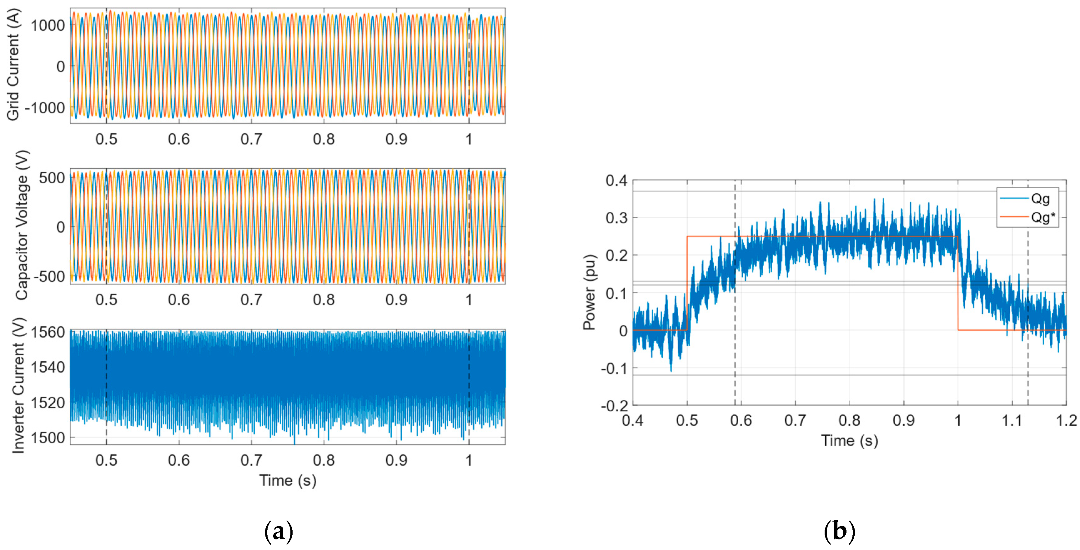
3.2. Transient Response

The inverter’s transient response was first evaluated using a single step change in reference real power P g from 1 pu to 0.25 pu at 0.5 s, with a subsequent step change from 0.25 pu to 1 pu at 1 s, while reference reactive power Q g remained fixed at 0 pu.
Grid current i g , capacitor voltage C i , and inverter current i d c waveforms are presented in Figure 7a, with both step changes indicated by a pair of dotted vertical lines. Grid current i g drops gradually in response to the step change in reference real power P g , while capacitor voltage C i remains stable and DC current i d c increases to a maximum of 1615.05 A.
Real power P g ’s waveform is presented in Figure 7b, with upper and lower bounds of ±0.12 pu indicated by a pair of solid horizontal lines above and below reference real power P g . Real power P g displays a settling time of 274.51 ms and 118.92 ms in response to the first and second step changes in reference real power P g , respectively.
The inverter’s transient response was then evaluated using a single step change in reference real power Q g from 0 pu to 0.25 pu at 0.5 s, with a subsequent step change from 0.25 pu to 0 pu at 1 s, while reference real power P g remained fixed at 1 pu. Grid current i g , capacitor voltage C i , and inverter current i d c waveforms are presented in Figure 8a, with both step changes indicated by a pair of vertical dotted lines. Grid current i g and capacitor voltage C i remain stable, while DC current i d c reaches a maximum of 1561.19 A.
Reactive power Q g ’s waveform is presented in Figure 8b, with upper and lower bounds of ±0.12 pu indicated by a pair of horizontal solid lines above and below reference real power Q g . Real power Q g displays a settling time of 88.40 ms and 129.21 ms in response to the first and second step changes in reference real power Q g , respectively.
A summary of the results collected during transient conditions, along with comparisons to steady-state operation under normal grid conditions and fault conditions, may be found in Table 3 below.

3.3. Fault Response

The inverter’s fault response was first evaluated under line–ground (L-G), line–line–ground (L-L-G), and line–line–line–ground (L-L-L-G) fault conditions, under strong grid conditions; that is, using parameters R s 1 and L s 1 , found in Table 1. Each fault was simulated for a duration of three cycles, or 50 ms, at a fixed reference real power P g of 0.7 pu and a fixed reference reactive power Q g of 0 pu.
Grid current i g , capacitor voltage C i , and the DC current i d c waveforms under L-G fault conditions are presented in Figure 9a, with fault conditions enclosed using a pair of vertical dotted lines. Grid current i g reaches a maximum of 2826.50 A in the fault-affected phase (Phase A) during fault conditions, while capacitor voltage C i ’s waveform is disrupted in the affected phase during fault conditions. The DC current i d c reaches a maximum of 1607.35 A.
Real power P g and reactive power Q g ’s waveforms under L-G fault conditions, along with their respective references, are presented in Figure 9b, along with bounds of ±0.12 pu above and below their reference values, indicated using a pair of solid horizontal lines, with fault conditions enclosed by a pair of vertical dotted lines. Real power P g and reactive power Q g reach a maximum of 1.70 pu and a minimum of −1.20 pu, respectively, during fault conditions, but return to steady-state bounds with a settling time of 61.67 ms and 20.61 ms, respectively, indicated using a vertical dotted line in each case to represent the system’s settling time.
Grid current i g , capacitor voltage C i , and the DC current i d c waveforms under L-L-G fault conditions are presented in Figure 10a, with fault conditions enclosed using a pair of dotted lines. Grid current i g reaches a maximum of 3564.71 A and 2606.32 A in the fault-affected phases (Phases A & B) during fault conditions, while capacitor voltage C i ’s waveform is disrupted in the affected phases during fault conditions. The DC current i d c reaches a maximum of 1593.67 A.
Real power P g and reactive power Q g ’s waveforms under L-L-G fault conditions, along with their respective references, are presented in Figure 10b, along with bounds of ±0.12 pu above and below their reference values, indicated using a pair of horizontal solid lines, with fault conditions enclosed by a pair of vertical dotted lines. Real power P g and reactive power Q g reach a maximum of 1.84 pu and 1.42 pu, respectively, during fault conditions, but return to steady-state bounds with a settling time of 94.06 ms and 25.95 ms, respectively. A vertical dotted line is used in each case to represent the system’s settling time.
Grid current i g   , capacitor voltage C i , and the DC current i d c waveforms under L-L-L-G fault conditions are presented in Figure 11a, with fault conditions enclosed using a pair of dotted lines. Grid current i g reaches a maximum of 4290.47 A, 2321.01 A, and 2286.37 A in the fault-affected phases (Phases A, B, and C) during fault conditions, while capacitor voltage C i ’s waveform is disrupted in the affected phases during fault conditions. The DC current i d c reaches a maximum of 1712.27 A.
Real power P g and reactive power Q g ’s waveforms under L-L-L-G fault conditions, along with their respective references, are presented in Figure 11b, along with bounds of ±0.12 pu above and below their reference values, indicated using a pair of horizontal solid lines, with fault conditions enclosed by a pair of vertical dotted lines. Real power P g and reactive power Q g reach a maximum of 2.25 pu and a minimum of −1.38 pu respectively, during fault conditions, but return to steady-state bounds with a settling time of 219.58 ms and 241.05 ms, respectively. A vertical dotted line is used in each case to represent the system’s settling time.
The inverter’s fault response was then evaluated under L-L-L-G fault conditions, under weak grid conditions; that is, using parameters R s 2 and L s 2 , found in Table 1. The fault was simulated for a duration of three cycles, or 50 ms, at a fixed reference real power P g of 0.7 pu and a fixed reference reactive power Q g of 0 pu.
Grid current i g , capacitor voltage C i , and the DC current i d c waveforms under L-L-L-G fault and weak grid conditions are presented in Figure 12a, with fault conditions enclosed using a pair of dotted lines. Grid current i g reaches a maximum of 4070.67 A, 2534.34 A, and 2428.82 A in the fault-affected phases (Phases A, B, and C) during fault conditions, while capacitor voltage C i ’s waveform is disrupted in the affected phases during fault conditions. The DC current i d c reaches a maximum of 1747.62 A.
Real power P g and reactive power Q g ’s waveforms under L-L-L-G fault and weak grid conditions, along with their respective references, are presented in Figure 12b, along with bounds of ±0.12 pu above and below their reference values, indicated using a pair of horizontal solid lines, with fault conditions enclosed by a pair of vertical dotted lines. Real power P g and reactive power Q g reach a maximum of 2.23 pu and a minimum of −0.98 pu, respectively, during fault conditions, but return to steady-state bounds with a settling time of 134.82 ms and 35.80 ms, respectively. A vertical dotted line is used in each case to represent the system’s settling time.
A summary of the results collected during fault conditions, along with comparisons to steady-state operation under normal grid conditions and transient conditions, may be found in Table 4 below.

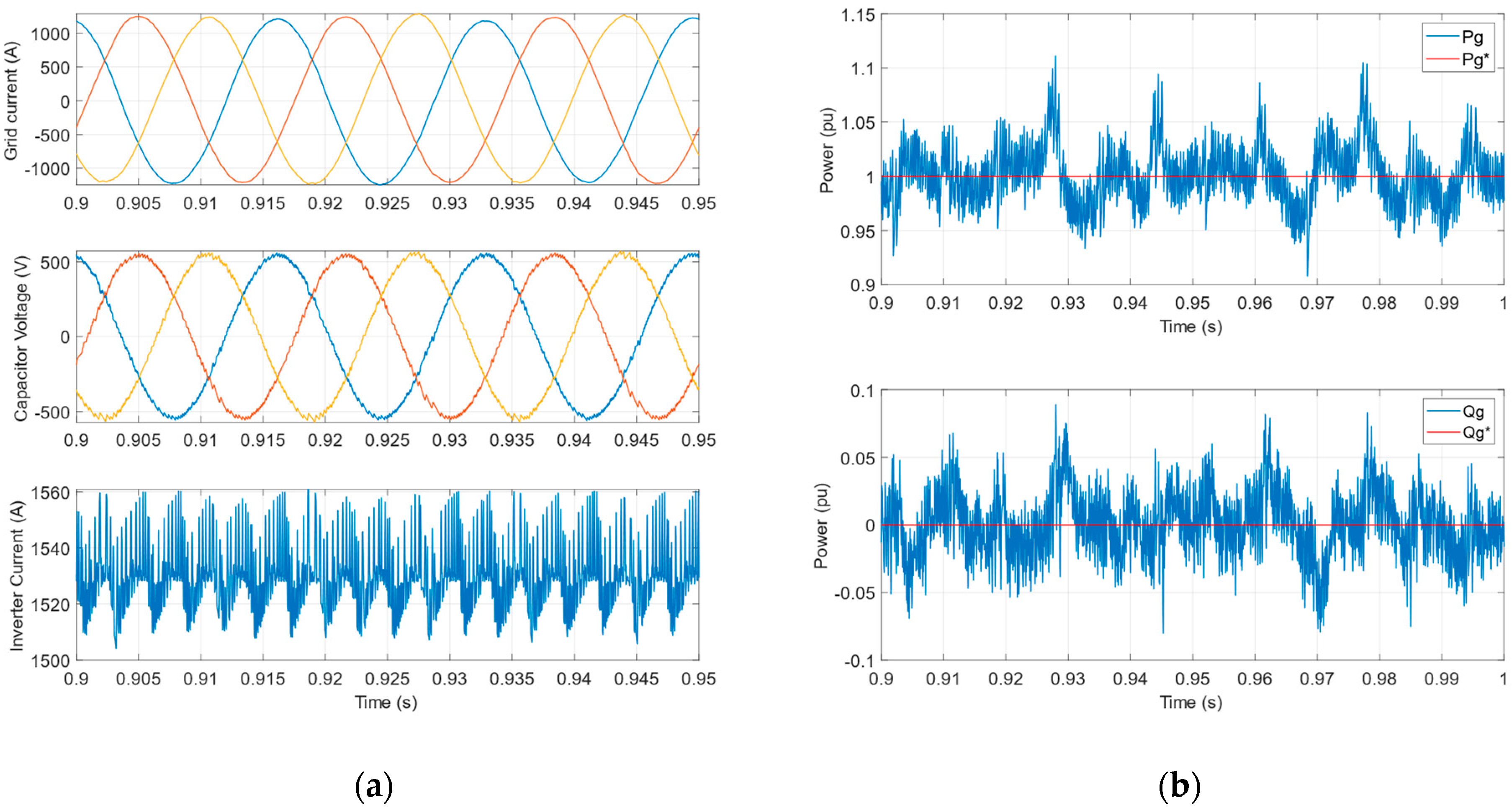
3.4. Comparison to Classic Linear Control

In the interests of highlighting the advantages of the HMPC approach to inverter control in contrast with classic linear droop control, the two approaches were simulated and compared under a three-cycle L-G fault condition, with reference real power P g set to 0.7 pu and reference reactive power Q g set to 0 pu, as well as a switching frequency of 2520 Hz in both cases. A side-by-side comparison of three-phase grid current i g , three-phase capacitor voltage C i , and DC-inverter-side current i d c may be found in Figure 13, with fault conditions enclosed using a pair of vertical dotted lines. A side-by-side comparison of real and reactive power P g and Q g waveforms may be found in Figure 14, with fault conditions enclosed using a pair of vertical dotted lines, and bounds of ±0.12 pu above and below their reference values, indicated using a pair of horizontal solid lines. Settling times are indicated using a single vertical dotted line. A summary of relevant results with comparisons between the two methods may be found in Table 5 below.

4. Discussion

In this paper, an HMPC approach was developed for the control of a GFM, buck-type CSI. The proposed control approach does away with some of the disadvantages/complexities of existing control methodologies while retaining the advantages of CSI topology, particularly in the context of their use in microgrid technology.
Based on the results of MATLAB/Simulink simulation, we found that the HMPC approach achieves satisfactory steady-state and dynamic performance in forming grid voltage and regulating real and reactive power, and in all cases, represents an improvement over a simple, linear droop-control approach. In addition, the developed control methodology demonstrates low-voltage ride-through capabilities under multiple grid fault conditions. Furthermore, thanks to CSIs’ inherent current-limiting characteristics, the current passing through the switching devices is limited to reasonable levels, regardless of whether they occur under normal or grid-fault conditions. In addition, the device’s settling time improves in the worst case (L-L-L-G fault conditions), under weak grid conditions, which more closely resemble the conditions found in microgrid-type applications, potentially preventing the need for a black start under fault conditions.
These results demonstrate that a buck-type CSI in conjunction with an HMPC control approach has high potential to be utilized as a competent and simple alternative to existing GFM control methodologies together with existing VSI-based solutions.
Future work will focus on the hardware testing and verification of the proposed GFM buck-type CSI using the HMPC approach described herein, and the use of additional control strategies to reduce unwanted power oscillations during fault conditions. In addition, though this study compares the HMPC approach in a single existing category of GFLI/GFMI control (linear droop control), there remain abundant opportunities to compare this approach with other control methodologies found in the literature, such as approaches based on reinforcement learning, and potentially implement facets of these strategies into the approach described herein.

Author Contributions

Conceptualization, H.G.; methodology and validation, H.G. and G.A.-L.; formal analysis, H.G. and G.A.-L.; investigation, H.G.; resources, H.G.; data curation, H.G. and G.A.-L.; writing—original draft preparation, H.G.; writing—review and editing, G.A.-L.; visualization, G.A.-L.; supervision, H.G.; project administration, H.G.; funding acquisition, H.G. All authors have read and agreed to the published version of the manuscript.

Funding

Washington State University Vancouver Research Mini Grant/Award Number: PG00019891.

Data Availability Statement

The original contributions presented in the study are included in the article, further inquiries can be directed to the corresponding author.

Conflicts of Interest

The authors declare no conflicts of interest.

References

  1. Lin, Y.; Eto, J.; Johnson, B.; Flicker, J.; Lasseter, R.; Pico, H.V.; Seo, G.-S.; Pierre, B.; Ellis, A. Research Roadmap on Grid-Forming Inverters. 2020. Available online: https://docs.nrel.gov/docs/fy21osti/73476.pdf (accessed on 28 May 2025).
  2. Matevosyan, J.; Badrzadeh, B.; Prevost, T.; Quitmann, E.; Ramasubramanian, D.; Urdal, H.; Achilles, S.; Macdowell, J.; Huang, S.H.; Vital, V.; et al. Grid-Forming Inverters: Are They the Key for High Renewable Penetration? IEEE Power Energy Mag. 2019, 17, 89–98. [Google Scholar] [CrossRef]
  3. Lasseter, R.H.; Chen, Z.; Pattabiraman, D. Grid-Forming Inverters: A Critical Asset for the Power Grid. IEEE J. Emerg. Sel. Top. Power Electron. 2020, 8, 925–935. [Google Scholar] [CrossRef]
  4. Simulating the Role of Grid-Forming Inverters in the Future Electric Grid. Available online: https://www.pnnl.gov/news-media/simulating-role-grid-forming-inverters-future-electric-grid (accessed on 4 July 2025).
  5. Geekiyanage, V.; Seppänen, J. Power System Stability Improvements Through Grid Forming Inverters for Systems with High Penetration of Grid Following Inverters. In Proceedings of the 2024 IEEE PES Innovative Smart Grid Technologies Europe (ISGT EUROPE), Dubrovnik, Croatia, 14–17 October 2024; pp. 1–5. [Google Scholar]
  6. Zhang, H.; Xiang, W.; Lin, W.; Wen, J. Grid Forming Converters in Renewable Energy Sources Dominated Power Grid: Control Strategy, Stability, Application, and Challenges. J. Mod. Power Syst. Clean Energy 2021, 9, 1239–1256. [Google Scholar] [CrossRef]
  7. Rathnayake, D.B.; Akrami, M.; Phurailatpam, C.; Me, S.P.; Hadavi, S.; Jayasinghe, G.; Zabihi, S.; Bahrani, B. Grid Forming Inverter Modeling, Control, and Applications. IEEE Access 2021, 9, 114781–114807. [Google Scholar] [CrossRef]
  8. Mirmohammad, M.; Azad, S.P. Control and Stability of Grid-Forming Inverters: A Comprehensive Review. Energies 2024, 17, 3186. [Google Scholar] [CrossRef]
  9. Wang, Z.; Zhao, S.; Li, Y.; Yang, F.; Zhao, Z. Fault Tolerant Control of Grid Connected Inverters Based on Low-Voltage Ride Through. Int. J. Mech. Electr. Eng. 2024, 3, 78–83. [Google Scholar] [CrossRef]
  10. Rathnayake, D.B.; Razzaghi, R.; Bahrani, B. Generalized Virtual Synchronous Generator Control Design for Renewable Power Systems. IEEE Trans. Sustain. Energy 2022, 13, 1021–1036. [Google Scholar] [CrossRef]
  11. Pattabiraman, D. Current Source Inverter with Grid Forming Control. Electr. Power Syst. Res. 2024, 226, 109910. [Google Scholar] [CrossRef]
  12. Fidone, G.L.; Migliazza, G.; Carfagna, E.; Benatti, D.; Immovilli, F.; Buticchi, G.; Lorenzani, E. Common Architectures and Devices for Current Source Inverter in Motor-Drive Applications: A Comprehensive Review. Energies 2023, 16, 5645. [Google Scholar] [CrossRef]
  13. Wu, B.; Pontt, J.; Rodriguez, J.; Bernet, S.; Kouro, S. Current-Source Converter and Cycloconverter Topologies for Industrial Medium-Voltage Drives. IEEE Trans. Ind. Electron. 2008, 55, 2786–2797. [Google Scholar] [CrossRef]
  14. Wu, B.; Lang, Y.; Zargari, N.; Kouro, S. Power Conversion and Control of Wind Energy Systems, 1st ed.; Wiley: Hoboken, NJ, USA, 2011; ISBN 978-0-470-59365-3. [Google Scholar]
  15. Vazquez, S.; Leon, J.I.; Franquelo, L.G.; Rodriguez, J.; Young, H.A.; Marquez, A.; Zanchetta, P. Model Predictive Control: A Review of Its Applications in Power Electronics. IEEE Ind. Electron. Mag. 2014, 8, 16–31. [Google Scholar] [CrossRef]
  16. Young, H.A.; Marin, V.A.; Pesce, C.; Rodriguez, J. Simple Finite-Control-Set Model Predictive Control of Grid-Forming Inverters With LCL Filters. IEEE Access 2020, 8, 81246–81256. [Google Scholar] [CrossRef]
  17. Gao, H.; Mahmud, T. High-Frequency Common-Mode Voltage Reduced Space Vector Modulation for Grid-Connected Current-Source Inverter. World Electr. Veh. J. 2022, 13, 236. [Google Scholar] [CrossRef]
  18. Wu, B.; Narimani, M. High-Power Converters and AC Drives, 2nd ed.; Wiley: Hoboken, NJ, USA, 2016; Available online: https://www.wiley.com/en-us/High-Power+Converters+and+AC+Drives%2C+2nd+Edition-p-9781119156031 (accessed on 4 July 2025).
Figure 1. Schematic diagram of a buck-type current-source inverter.
Energies 18 04124 g001
Figure 2. Control block diagram of grid-form buck-type CSI with HMPC.
Energies 18 04124 g002
Figure 3. Flowchart illustrating the control logic contained within the HMPC module seen in Figure 2.
Energies 18 04124 g003
Figure 4. Steady-state simulation results under normal grid conditions: (a) grid current, capacitor voltage, inverter current, and (b) real and reactive power.
Energies 18 04124 g004
Figure 5. Steady-state simulation results under unbalanced three-phase voltage conditions: (a) grid current, capacitor voltage, inverter current, and (b) real and reactive power.
Energies 18 04124 g005
Figure 6. Steady-state simulation results under an unbalanced X / R ratio of 20: (a) grid current, capacitor voltage, inverter current, and (b) real and reactive power.
Energies 18 04124 g006
Figure 7. Simulation results in response to step change in reference real power P g : (a) grid current, capacitor voltage, inverter current, and (b) real power.
Energies 18 04124 g007
Figure 8. Simulation results in response to step change in reference reactive power Q g : (a) grid current, capacitor voltage, inverter current, and (b) reactive power.
Energies 18 04124 g008
Figure 9. Simulation results under L-G fault conditions: (a) grid current, capacitor voltage, inverter current, and (b) real and reactive power.
Energies 18 04124 g009
Figure 10. Simulation results under L-L-G fault conditions: (a) grid current, capacitor voltage, inverter current, and (b) real and reactive power.
Energies 18 04124 g010
Figure 11. Simulation results under L-L-L-G fault conditions: (a) grid current, capacitor voltage, inverter current, and (b) real and reactive power.
Energies 18 04124 g011
Figure 12. Simulation results under L-L-L-G fault conditions and weak grid conditions: (a) grid current, capacitor voltage, inverter current, and (b) real and reactive power.
Energies 18 04124 g012
Figure 13. Grid current, capacitor voltage, and inverter current under L-G fault conditions using a (a) droop-control approach and using an (b) MPC approach.
Energies 18 04124 g013
Figure 14. Real and reactive power under L-G fault conditions using a (a) linear droop-control approach and using an (b) HMPC approach.
Energies 18 04124 g014
Table 1. Comparison between relevant control methodologies.
Control
Methodology
Current-LimitingSimple Control
Algorithm
PLL Independent
D r o o p   C o n t r o l
V S G   C o n t r o l
V O B   C o n t r o l
d V O B   C o n t r o l
MPC
Table 2. Simulation parameters.
ParameterValueParameterValue
R s 1 0.01 pu I d c 1.1 pu
L s 1 0.1 pu V c i 0 1.0 pu
R s 2 0.05 pu ω 0 377 rad/s
L s 2 0.5 pu m 0.01
C i 0.15 pu n 0.05
L d c 0.95 pu ω c 50 rad/s
V d c 1.0 pu T s 50 μs
The parameters R s 1 and L s 1 represent strong grid conditions, where equivalent resistance and impedance are relatively low. R s 2 and L s 2 represent weak grid conditions, where equivalent resistance and impedance are relatively high. Unless otherwise noted, all simulation results are generated using strong grid conditions.
Table 3. Comparison between steady state under ideal and non-ideal grid conditions.
ConditionsTHD ( i g )THD ( C v )Max i d c Max/min P g Max/min Q g F s w
Normal1.52%2.57%1561.65 A1.11 pu0.12 pu2489 Hz
Unbalanced Three-Phase Voltage7.01%5.37%1568.12 A1.34 pu0.35 pu2199 Hz
X/R Ratio: 201.51%2.41%1560.90 A1.11 pu−0.10 pu2514 Hz
Table 4. Summary of inverter operation under steady-state, transient, and fault conditions.
Condition Max   i g Max   C v Max   i d c Max / Min   P g Max / Min   Q g T s p T s q
Steady-staten/an/a1561.65 A1.11 pu0.12 pun/an/a
Transient   P g * 401.05 An/a1615.05 An/an/a274.51 ms
118.92 ms
n/a
Transient   Q g * n/an/a1561.19 An/an/an/a88.40 ms
129.21 ms
L-G Fault2826.50 A
1148.99 A
1605.57 A
n/a1607.35 A1.70 pu−1.20 pu61.67 ms20.61 ms
L-L-G Fault3564.71 A
2606.32 A
1909.11 A
n/a1593.67 A1.84 pu1.42 pu94.06 ms25.95 ms
L-L-L-G Fault4290.47 A
2321.01 A
2286.37 A
n/a1712.27 A2.25 pu−1.38 pu219.58 ms241.05 ms
L-L-L-G Fault
(Weak Grid)
4070.67 A
2534.34 A
2428.82 A
n/a1747.62 A2.23 pu0.98 pu134.82 ms35.80 ms
Table 5. Comparison between an existing droop-control model and the current MPC-based model’s L-G fault response.
Model Max   i g Max   C v Max   i d c Max   P g Max   Q g T s p T s q
Droop Control2967.60 A805.90 V1599.80 A2.65 pu1.59 pu69.06 ms200.68 ms
Buck-Type MPC2870.30 A550.04 V958.33 A1.74 pu1.19 pu50.66 ms21.46 ms
Maximum grid current i g and maximum capacitor voltage C V represent only the current and voltage of the affected phase, respectively; in this case, Phase A.
Disclaimer/Publisher’s Note: The statements, opinions and data contained in all publications are solely those of the individual author(s) and contributor(s) and not of MDPI and/or the editor(s). MDPI and/or the editor(s) disclaim responsibility for any injury to people or property resulting from any ideas, methods, instructions or products referred to in the content.

