
A Multi-Step Topological Optimization Approach for Spacer Shape Design in Double-Sided SiC MOSFET Power Modules Considering Thermo-Mechanical Effects


Abstract
1. Introduction
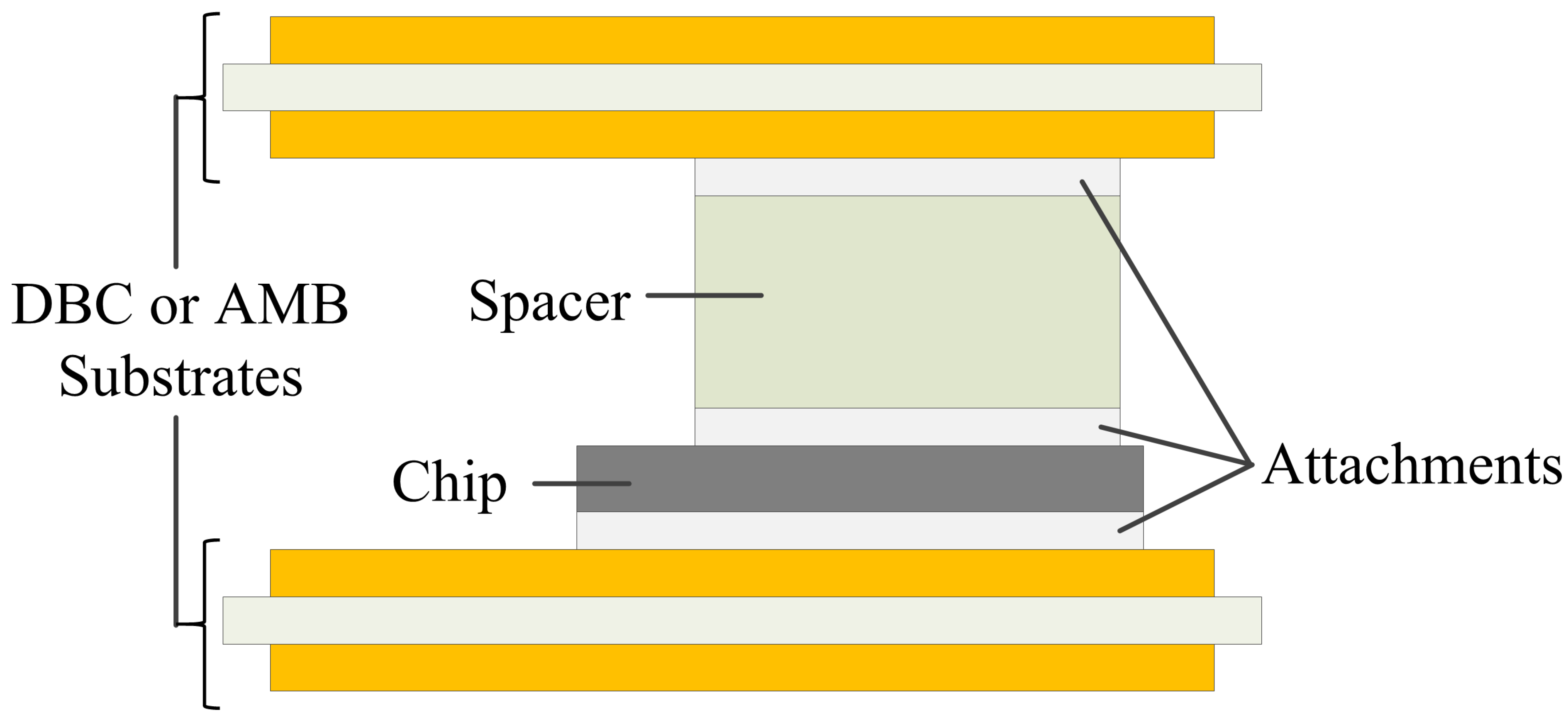
2. Methodologies
- (1)
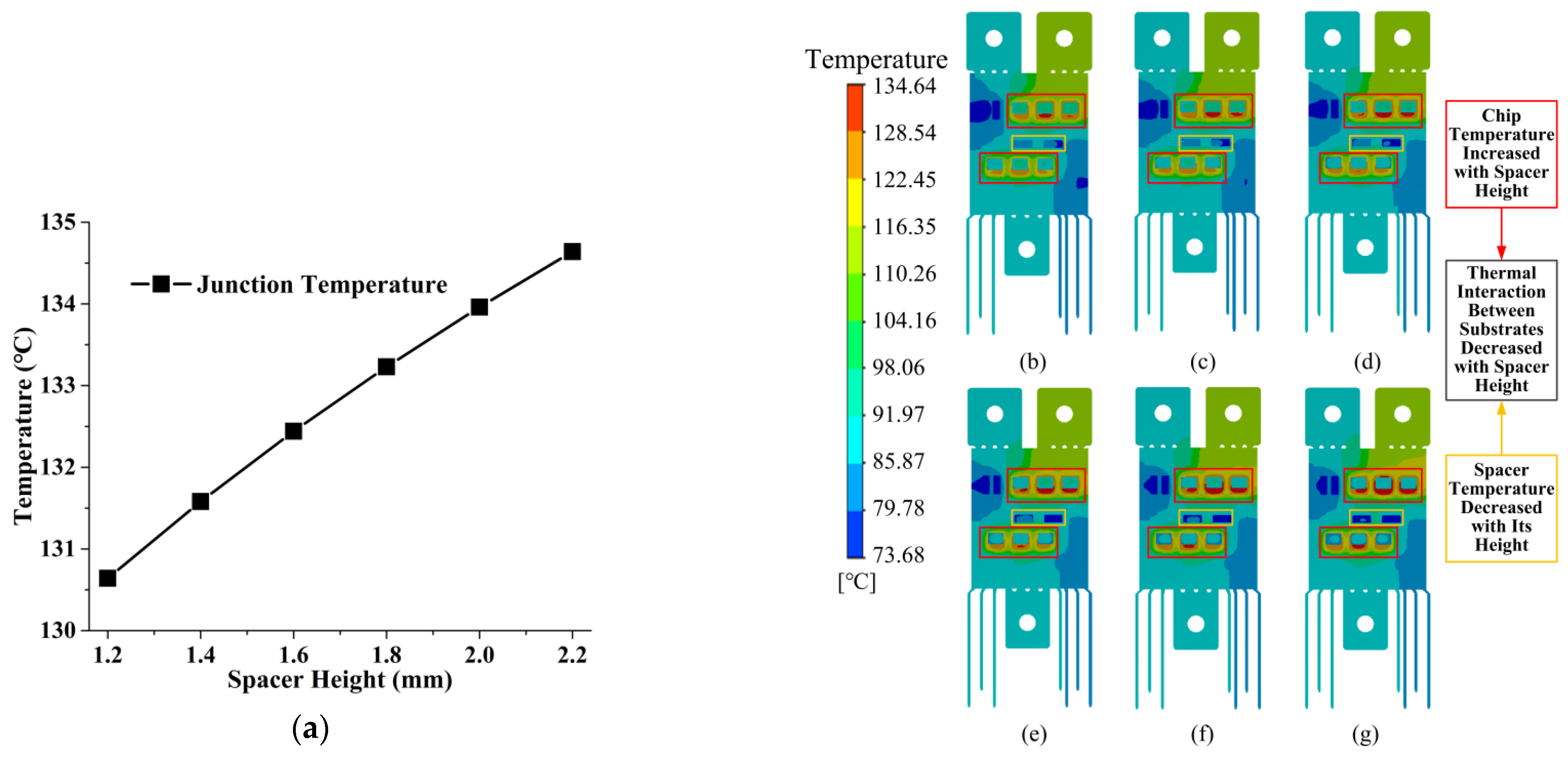
- As the TOs are conducted with the governing variable θc varied in the tessellated and fixed grids [23,24,25], the influences of spacer height variations will have to be analyzed in multiple TOs with different spacer models and grids; therefore, increasing significantly the computational cost. To handle this problem, first, comparative numerical analyses are simulated based on conventional brick-shaped spacers with different heights, and the proper height is selected and predetermined in the first step.
- (2)
- Since the spacers are utilized to buffer the thermo-mechanical stresses, which may influence the working performances of the devices or even result in failures [29], the stress-related global variable, for example, the strain energy ws, should be considered in the optimization target function. However, whether to simply use the strain energy in the chip-substrate attachment ws_attachment or take the other components ws_others into consideration should also be analyzed. To better balance the optimization convergence and the optimization effectiveness [29], in the second step, the influence of the weight factors is investigated, and the weighted objective combinations are formulated as follows:where β is the weight factor. When β = 1, the objective function is the total strain energy, and when β = 0, only the strain energy in the attachment is considered.
- (3)
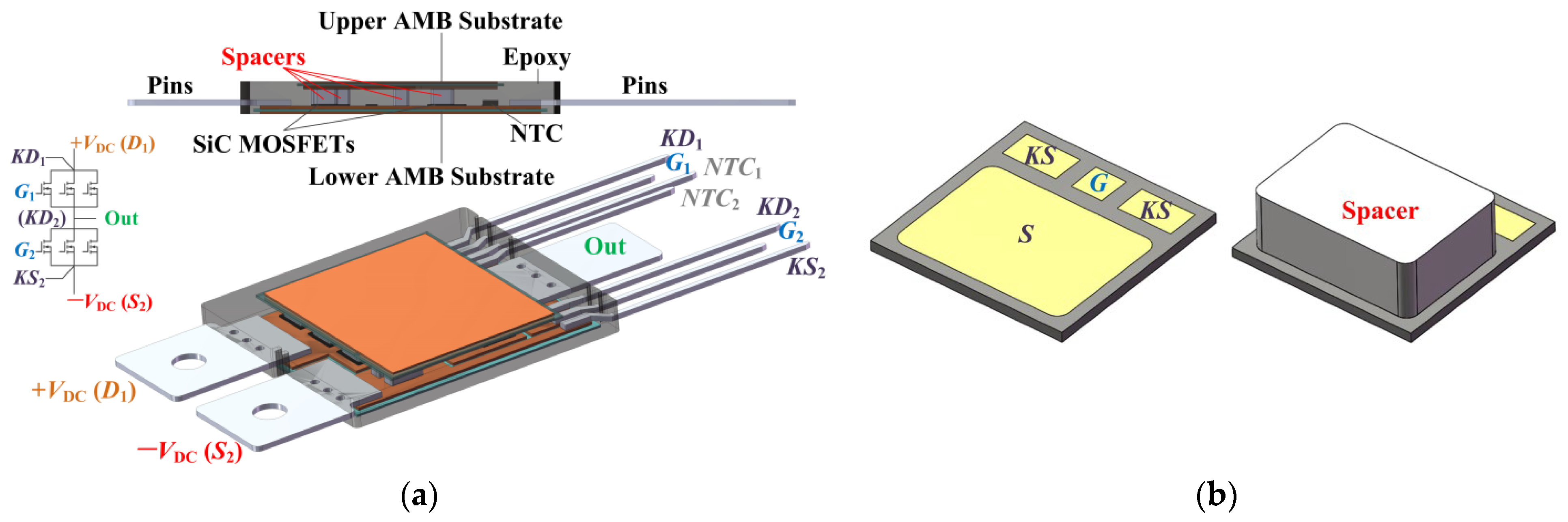
- In addition to the spacer height and the optimization objective function, the TO region of the spacers should be limited with a non-optimized spacer frame to guarantee basic electric and thermal conductivity. For 2D TOs, the non-optimized spacer frame and optimized spacer filling structure can be simple, but the 3D ones can be divided into two categories: (I) a spacer frame with two longitudinally placed fillers sandwiching the pillar of the frame, and (II) a frame with transversely located fillers. The spacer combination models are illustrated in Table 1. Based on the TO results, the preferable spacer combination structure is decided.
- (4)
- In step 4, the TO based on the power module’s full domain model with the spacer height determined in step 1, the optimization target function decided in step 2, and the preferable spacer combination structure settled in step 3, is conducted to output the final optimized spacer structure.
3. Step I: Thermo-Mechanical Coupled Analyses and Spacer Height Determination
4. Step II: 2D Spacer TO Design and Objective Function Determination
4.1. Total Strain Energy in Whole Region (β = 1)
4.2. Strain Energy in Chip-Substrate Attachment (β = 0)
4.3. Weighted Strain Energy Combinations (β = 0.2, 0.4, 0.6, 0.8)
5. Step III: 3D Spacer Combination Structure Determination
5.1. Spacer Frame with Longitudinally Arranged Fillings
5.2. Spacer Frame with Transversely Arranged Fillings
6. Step IV: 3D Spacer TO Design Based on a Full Domain Model
6.1. Three-Dimensional Spacer TO Design and Discussion
6.2. Lifetime Predictions
7. Conclusions
Author Contributions
Funding
Data Availability Statement
Conflicts of Interest
Abbreviations
| TO | Topology optimization |
| WBG | Wide bandgap |
| SiC | Silicon carbide |
| GaN | Gallium nitride |
| DSC | Double-sided cooled |
| MOSFET | Metal-oxide-semiconductor field-effect transistor |
| 2D | Two-dimensional |
| 3D | Three-dimensional |
| SIMP | Solid isotropic material with penalization |
| MMAs | Method of moving asymptotes |
References
- Li, B.Y.; Yang, X.; Wang, K.P.; Zhu, H.K.; Wang, L.L.; Chen, W.J. A compact double-sided cooling 650V/30A GaN power module with low parasitic parameters. IEEE Trans. Power Electron. 2022, 37, 426–439. [Google Scholar] [CrossRef]
- Han, L.B.; Liang, L.; Zhang, Z.Y.; Kang, Y. Understanding inherent implication of thermal resistance in double-side cooling module. IEEE Trans. Power Electron. 2023, 38, 2435–2445. [Google Scholar] [CrossRef]
- Peng, C.; Zhu, W.H.; Ke, P.; Li, R.; Dai, X.P.; Wang, L.C. Investigation of vehicle-oriented double-sided cooling power module with BGA technology. IEEE J. Emerg. Sel. Top. Power Electron. 2022, 10, 6171–6179. [Google Scholar] [CrossRef]
- Peng, C.; Huang, Q.; Qi, F.; Ke, P.; Dai, X.P.; Zhu, W.H.; Wang, L.C. Investigation on the reliability of die-attach structures for double-sided cooling power module. IEEE Trans. Compon. Packag. Manuf. Technol. 2021, 11, 793–801. [Google Scholar] [CrossRef]
- Liu, M.; Coppola, A.; Alvi, M.; Anwar, M. Comprehensive review and state of development of double-sided cooled package technology for automotive power modules. IEEE Open J. Power Electron. 2022, 3, 271–289. [Google Scholar] [CrossRef]
- Haque, S.; Xing, K.; Lin, R.L.; Suchicital, C.T.A.; Lu, G.Q.; Nelson, D.J.; Borojevic, D.; Lee, F.C. An innovative technique for packaging power electronic building blocks using metal posts interconnected parallel plate structures. IEEE Trans. Adv. Packag. 1999, 22, 136–144. [Google Scholar] [CrossRef]
- Catalano, A.P.; Scognamillo, C.; d’Alessandro, V.; Castellazzi, A. Numerical simulation and analytical modeling of the thermal behavior of single- and double-sided cooled power modules. IEEE Trans. Compon. Packag. Manuf. Technol. 2020, 10, 1446–1453. [Google Scholar] [CrossRef]
- Sun, P.; Niu, F.L.; Zeng, Z.; Li, H.Y.; Ou, H.H. FEA-dominant reliability and lifetime model of double-sided cooling SiC power module. IEEE Trans. Device Mater. Reliab. 2023, 23, 178–186. [Google Scholar] [CrossRef]
- Ding, C.; Liu, H.Z.Q.; Ngo, K.D.T.; Burgos, R.; Lu, G.Q. A double-side cooled SiC MOSFET power module with sintered-Silver interposers: I-design, simulation, fabrication, and performance characterization. IEEE Trans. Power Electron. 2021, 36, 11672–11680. [Google Scholar] [CrossRef]
- Wang, M.Y.; Mei, Y.H.; Liu, W.; Xie, Y.J.; Fu, S.C.; Li, X.; Lu, G.Q. Reliability improvement of a double-sided IGBT module by lowering stress gradient using molybdenum buffers. IEEE J. Emerg. Sel. Top. Power Electron. 2019, 7, 1637–1648. [Google Scholar] [CrossRef]
- Cao, J.L.; Li, J.; Mei, Y.H. A double-sided bidirectional power module with low heat concentration and low thermomechanical stress. IEEE Trans. Power Electron. 2021, 36, 9763–9766. [Google Scholar] [CrossRef]
- Li, J.F.; Castellazzi, A.; Dai, T.X.; Corfield, M.; Solomon, A.K.; Johnson, C.M. Built-in reliability design of highly integrated solid-state power switches with metal bump interconnects. IEEE Trans. Power Electron. 2015, 30, 2587–2600. [Google Scholar]
- Jeon, J.; Seong, J.; Lim, J.; Kim, M.K.; Kim, T.; Yoon, S.W. Finite element and experimental analysis of spacer designs for reducing the thermomechanical stress in double-sided cooling power modules. IEEE J. Emerg. Sel. Top. Power Electron. 2021, 9, 3383–3391. [Google Scholar] [CrossRef]
- Zeng, Z.; Ou, K.H.; Wang, L.; Yu, Y. Reliability-oriented automated design of double-sided cooling power module: A thermo-mechanical-coordinated and multi-objective-oriented optimization methodology. IEEE Trans. Device Mater. Reliab. 2020, 20, 584–595. [Google Scholar] [CrossRef]
- Ji, B.; Song, X.G.; Sciberras, E.; Cao, W.P.; Hu, Y.H.; Pickert, V. Multiobjective design optimization of IGBT power modules considering power cycling and thermal cycling. IEEE Trans. Power Electron. 2015, 30, 2493–2504. [Google Scholar] [CrossRef]
- Qian, Y.C.; Hou, F.Z.; Fan, J.J.; Lv, Y.Q.; Fan, X.J.; Zhang, G.Q. Design of a fan-out panel-level SiC MOSFET power module using ant colony optimization-back propagation neural network. IEEE Trans. Electron. Devices 2021, 68, 3460–3467. [Google Scholar] [CrossRef]
- Wang, W.J.; Ho, S.L.; Fu, W.N. A multiscale topology optimization methodology based on sequential element rejection-admission and boundary element evolvement. IEEE Trans. Magn. 2019, 55, 7201304. [Google Scholar]
- Doi, S.; Sasaki, H.; Igarashi, H. Multi-Objective topology optimization of rotating machines using deep learning. IEEE Trans. Magn. 2019, 55, 7202605. [Google Scholar] [CrossRef]
- Jung, S.W.; Ro, J.S.; Jung, H.K. A hybrid algorithm using shape and topology optimization for the design of electric machines. IEEE Trans. Magn. 2018, 54, 8102604. [Google Scholar] [CrossRef]
- Xia, M.; Yang, S.Y.; Sykulski, J. A novel 3-D topology optimization methodology based on the min-cut theorem. IEEE Trans. Magn. 2021, 57, 7201005. [Google Scholar] [CrossRef]
- Santhanakrishnan, M.S.; Tilford, T.; Bailey, C. Multi-material heatsink design using level-set topology optimization. IEEE Trans. Compon. Packag. Manuf. Technol. 2019, 9, 1504–1513. [Google Scholar] [CrossRef]
- Lee, G.; Joo, Y.; Kim, S.J. On the objective function for topology optimization of heat sinks. IEEE Trans. Compon. Packag. Manuf. Technol. 2021, 11, 1776–1782. [Google Scholar] [CrossRef]
- Majdi, B.; Reza, A. Multi-Material topology optimization of compliant mechanisms via solid isotropic material with penalization approach and alternating active phase algorithm. Proc. Inst. Mech. Eng. Part C-J. Eng. Mech. Eng. Sci. 2020, 234, 2631–2642. [Google Scholar] [CrossRef]
- Li, L.N.; Zhu, G.J.; Wang, Z.; Liu, T.; Yang, S.Y. Topological design optimization approach for winding oil flow paths in oil-natural air-natural transformers based on a fluidic-thermal coupled model. IEEE Trans. Magn. 2023, 59, 8401405. [Google Scholar] [CrossRef]
- Ni, Q. A globally convergent method of moving asymptotes with trust region technique. Optim. Method Softw. 2003, 18, 283–297. [Google Scholar] [CrossRef]
- Wang, L.S.; Deng, J.Y.; Zeng, K.Q.; Cheng, H.G.; Wu, Q.; Lin, J.; Rietveld, G.; Hueting, R.J.E. Design and Fabrication of a Ceramic Substrate-Embedded SiC Power Module. IEEE Trans. Compon. Packag. Manuf. Technol. 2025, 15, 938–948. [Google Scholar] [CrossRef]
- Chang, Y.; Luo, H.Z.; Iannuzzo, F.; Bahman, A.S.; Li, W.H.; He, X.N.; Blaabjerg, F. Compact Sandwiched Press-Pack SiC Power Module With Low Stray Inductance and Balanced Thermal Stress. IEEE Trans. Power Electron. 2020, 35, 2237–2241. [Google Scholar] [CrossRef]
- Li, B.Y.; Yang, X.; Wang, K.P.; Wu, M.; Chen, W.J. Thermomechanical Stress Analysis, Characterization, and Optimization for Double-Side Cooled Power Modules With Ceramic Substrate. IEEE Trans. Compon. Packag. Manuf. Technol. 2024, 14, 561–572. [Google Scholar] [CrossRef]
- Xu, K.K. Silicon electro-optic micro-modulator fabricated in standard CMOS technology as components for all silicon monolithic integrated optoelectronic systems. J. Micromech. Microeng. 2021, 31, 054001. [Google Scholar] [CrossRef]
- Toenjes, A.; Zinn, C.; von Hehl, A.; Wang, H.C.; Hantzsche, K.; Hesselmann, M. Smart-Alloying for tailored microstructures in laser-based metal additive manufacturing. J. Laser Appl. 2025, 37, 054001. [Google Scholar] [CrossRef]
- Cheng, H.C.; Syu, J.Y.; Wang, H.H.; Liu, Y.C.; Kao, K.S.; Chang, T.C. Power Cycling Modeling and Lifetime Evaluation of SiC Power MOSFET Module Using a Modified Physical Lifetime Model. IEEE Trans. Device Mater. Reliab. 2024, 24, 142–153. [Google Scholar] [CrossRef]
- Ning, P.; Liu, J.; Wang, D.; Zhang, Y.; Li, Y. Assessing the Fatigue Life of SiC Power Modules in Different Package Structures. IEEE Access 2021, 9, 12074–12082. [Google Scholar] [CrossRef]


| Description | Model Shape |
|---|---|
| 2D Model |  |
| 3D Model (I) ---------------- Simplified Model with Spacer Using Longitudinal Fillings | 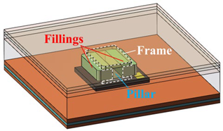 |
| 3D Model (II) ---------------- Simplified Model with Spacer Using Transverse Fillings | 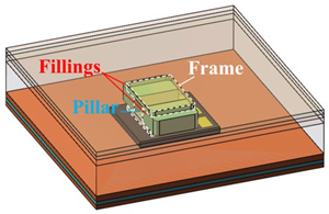 |
| No. | Model Shape | Description |
|---|---|---|
| Case 1 Original brick spacer |  | 2D simplified model with original brick-shaped spacer. |
| Case 2 Spacer frame |  | 2D simplified model with non-optimized spacer frame. |
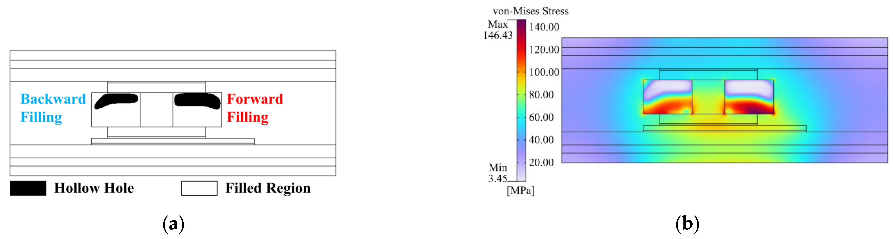
| Case 3 TO-designed spacer frame |  | 2D simplified model with TO optimized spacer frame (hollow holes dug in both forward and backward fillings). |
| Step | Max. Stress in Chip Attachments | Stress Reduction vs. Brick Spacer | Role of Each Step |
|---|---|---|---|
| I | 111.78 MPa | -- | Set the spacer height. |
| II | 98.37 MPa | 12.00% | Define the objective function. |
| III | 93.64 MPa | 16.23% | Establish spacer architecture. |
| IV | 90.07 MPa | 19.42% | Finalize the TO design. |
Disclaimer/Publisher’s Note: The statements, opinions and data contained in all publications are solely those of the individual author(s) and contributor(s) and not of MDPI and/or the editor(s). MDPI and/or the editor(s) disclaim responsibility for any injury to people or property resulting from any ideas, methods, instructions or products referred to in the content. |
© 2025 by the authors. Licensee MDPI, Basel, Switzerland. This article is an open access article distributed under the terms and conditions of the Creative Commons Attribution (CC BY) license (https://creativecommons.org/licenses/by/4.0/).
Share and Cite
Guo, Y.; Chen, K.; Jiang, W.; Li, L.; Zhu, G. A Multi-Step Topological Optimization Approach for Spacer Shape Design in Double-Sided SiC MOSFET Power Modules Considering Thermo-Mechanical Effects. Energies 2025, 18, 3850. https://doi.org/10.3390/en18143850
Guo Y, Chen K, Jiang W, Li L, Zhu G. A Multi-Step Topological Optimization Approach for Spacer Shape Design in Double-Sided SiC MOSFET Power Modules Considering Thermo-Mechanical Effects. Energies. 2025; 18(14):3850. https://doi.org/10.3390/en18143850
Chicago/Turabian StyleGuo, Yuhang, Ke Chen, Wentao Jiang, Longnv Li, and Gaojia Zhu. 2025. "A Multi-Step Topological Optimization Approach for Spacer Shape Design in Double-Sided SiC MOSFET Power Modules Considering Thermo-Mechanical Effects" Energies 18, no. 14: 3850. https://doi.org/10.3390/en18143850
APA StyleGuo, Y., Chen, K., Jiang, W., Li, L., & Zhu, G. (2025). A Multi-Step Topological Optimization Approach for Spacer Shape Design in Double-Sided SiC MOSFET Power Modules Considering Thermo-Mechanical Effects. Energies, 18(14), 3850. https://doi.org/10.3390/en18143850